EP0263530A2 - Bloch line memory device - Google Patents
Bloch line memory device Download PDFInfo
- Publication number
- EP0263530A2 EP0263530A2 EP87114799A EP87114799A EP0263530A2 EP 0263530 A2 EP0263530 A2 EP 0263530A2 EP 87114799 A EP87114799 A EP 87114799A EP 87114799 A EP87114799 A EP 87114799A EP 0263530 A2 EP0263530 A2 EP 0263530A2
- Authority
- EP
- European Patent Office
- Prior art keywords
- magnetic
- stripe
- domain
- bloch line
- bloch
- Prior art date
- Legal status (The legal status is an assumption and is not a legal conclusion. Google has not performed a legal analysis and makes no representation as to the accuracy of the status listed.)
- Granted
Links
Images


Classifications
-
- G—PHYSICS
- G11—INFORMATION STORAGE
- G11C—STATIC STORES
- G11C19/00—Digital stores in which the information is moved stepwise, e.g. shift registers
- G11C19/02—Digital stores in which the information is moved stepwise, e.g. shift registers using magnetic elements
- G11C19/08—Digital stores in which the information is moved stepwise, e.g. shift registers using magnetic elements using thin films in plane structure
- G11C19/0808—Digital stores in which the information is moved stepwise, e.g. shift registers using magnetic elements using thin films in plane structure using magnetic domain propagation
- G11C19/0841—Digital stores in which the information is moved stepwise, e.g. shift registers using magnetic elements using thin films in plane structure using magnetic domain propagation using electric current
-
- G—PHYSICS
- G11—INFORMATION STORAGE
- G11C—STATIC STORES
- G11C19/00—Digital stores in which the information is moved stepwise, e.g. shift registers
- G11C19/02—Digital stores in which the information is moved stepwise, e.g. shift registers using magnetic elements
- G11C19/08—Digital stores in which the information is moved stepwise, e.g. shift registers using magnetic elements using thin films in plane structure
Definitions
- the present invention relates to a Bloch line memory device, and more particularly to the structure of stripe magnetic domains which stores vertical Bloch lines as information carriers.
- a Bloch line memory device uses a magnetic garnet film as a memory medium.
- the magnetic garnet film is formed such that its film plane has a (111) face.
- an information storing manner is greatly different between both the devices. Namely, in the magnetic bubble memory device, the presence or absence of a bubble domain corresponds to information of "1" or "0".
- the Bloch line memory device on the other hand, the presence or absence of a pair of Bloch lines in a magnetic wall enclosing a stripe magnetic domain which has a stretched magnetic domain form, corresponds to informaiton of "1" " or "0". This situation is illustrated in Fig. 1.
- an upward arrow 103 in a stripe magnetic domain 2 existing in a magnetic garnet film 6 represents the direction of magnetization in the stripe magnetic domain 2
- an arrow 5 in a magnetic wall 1 represents the direction of magnetization of the magnetic wall 1.
- an arrow 101 on a center line in the magnetic wall 1 represents the direction of magnetization of the magnetic wall at a central portion of the magnetic wall 1.
- An arrow 102 perpendicular to the face of the magnetic wall 1 represents the direction of magnetization at a central portion of a vertical Bloch line (hereinafter referred to simply as Bloch line).
- a portion 4a where a pair of Bloch lines 3 exist corresponds to information of "1" while a portion 4b where no Bloch line exists corresponds to information of "0".
- the pair 4a of Bloch lines 3 used as an information carrier is a microstructure of domain wall which exists in the magnetic wall 1 enclosing the stripe magnetic domain 2, as is shown in Fig. 1.
- the Bloch lines 3 exist stably in the magnetic wall 1 and can move freely in the magnetic wall 1. Therefore, if a multiplicity of the stripe magnetic domains 2 are arranged in a juxtaposing manner with the Bloch lines 3 in the magnetic walls of the respective stripe magnetic domains, a memory section * tike a minor loop of the magnetic bubble memory can be constructed.
- Bloch lines are known for long, and experiments and analyses thereof have demonstrated that the speed of movement of a magnetic domain becomes slower because of the existence of Bloch lines.
- a magnetic domain including Bloch lines is called a hard bubble and efforts have been made to prevent the generation of such hard bubbles.
- Bloch line memory device the existence of Bloch lines are positively utilized.
- the physical dimension of a Bloch line is about one tenth of the width of a stripe magnetic domain having the Bloch line therein.
- Many Bloch lines can be included in one stripe magnetic domain.
- the stripe magnetic domain can involve about 5 x 10 8 Bloch lines per 1 cm 2 . Accordingly, when two Bloch lines are paired as an information carrier, a memory in the class of 256 Mbit/cm 2 can be fabricated.
- the Bloch lines have a reason other than the possession of its fine size why a memory having a large capacity can be provided. Namely, since in the Bloch line memory device a magnetic field in a direction perpendicular to a surface or film plane of the magnetic garnet film is used to propagate or transfer information though in the magnetic bubble memory device an information carrier is propagated by rotating an in-plane field, a propagation track pattern in the Bloch line memory device assumes a simplified planar configuration and construction, which facilitates an improvement in density of the deivce.
- FIG. 2 shows an example of the propagation track pattern.
- a Bloch line pair 4 exists in a magnetic wall enclosing a stripe magnetic domain 2 which is present in a magnetic garnet film 6 formed on a substrate 9.
- the stripe magnetic domain 2 exists to enclose a grooving 8 formed in a part of the magnetic garnet film 6.
- the grooving 8 is one means for arranging many stripe magnetic domains 2 in juxtaposition relation with each other and fixing their positions.
- the Bloch line pair 4 is moved in the magnetic wall 1 by a magnetic field Hpapplied perpendicularly to the surface of the magnetic garnet film 6. In order that the Bloch line pair 4 is moved by a fixed amount at this time, a propagation track pattern 7 is provided on the stripe magnetic domain 2.
- the Bloch line pair 4 is fixed by an in-plane field 104 having the same direction as the magnetization 105 of a region enclosed by the Bloch line pair.
- the Bloch line pair 4 can be moved below the next propagation track pattern 7.
- the requirement of the propagation track pattern 7 for realizing this operation is only to have a function of generating the in-plane field 104 and hence the pattern 7 may be provided by the repetition of a simple rectangular shape, as shown in Fig. 2.
- the Bloch line pair as an information carrier can freely move around the stripe magnetic domain.
- a Bloch line memory is schematically shown in Fig. 3.
- the memory section is constructed a multiplicity of juxtaposed stripe magnetic domains 2.
- the propagation track pattern 7 is provided crossing at an approximately right angle with respect to the stripe magnetic domains 2.
- Read and write function sections 121 and 120 are provided at the right and left sides of the stripe magnetic domains 2, respectively.
- Bloch lines are effected by causing a current to flow through a conductor formed in the vicinity of a left end portion of the stripe magnetic domain 2 to generate a localized magnetic field so that the magnetization of the magnetic wall is inverted by 180°. Namely, the magnetization of the region 4b of "0" shown in Fig. 1 is inverted so as to take the direction of magnetization of the portion 4a of "1". At this time, the magnetization continuously changes at an interface between the inverted region and a non-inverted region to produce a state in which the magnetization is changed by 90° with respect to the magnetic wall. This state yields a Bloch line.
- Such Bloch lines are necessarily produced in a paired form and hence a memory is constructed by corresponding a pair of Bloch lines to one unit of information.
- the write function section 120 is provided with a magnetic bubble transfer track 110 and a magnetic bubble generator 11.
- the magnetic bubble propagation track 110 transfers a magnetic bubble 10 from the magnetic bubble generator 11 to the left side of a predetermined stripe magnetic domain 2.
- the reading of information is effected by converting the presence or absence of Bloch lines into the presence or absence of a magnetic bubble.
- the chopping of a magnetic bubble from the stripe magnetic domain can be made only in the case where one Bloch line is present at the end portion of the stripe magnetic domain.
- This chopping is carried out at the read function section 121.
- the chopped magnetic bubble is transferred through a propagation track 111 for read-out to a magnetic bubble detector 12 by which the presence of the magnetic bubble is converted into an electric signal.
- the presence or absence of this electric signal corresponds to the presence or absence of the magnetic bubble and hence the presence or absence of the Bloch lines (i.e. information) at the end portion of a predetermined stripe magnetic domain. In this way, the reading operation is carried out.
- a Bloch line memory device is described in detail by U.S. Patent 4,583,200.
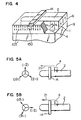
- Fig. 4 is a view showing the state of a stripe magnetic domain 2 existing in a magnetic garnet film 6 formed on a substrate 9.
- a Bloch line pair 4 is present in a magnetic wall 1 of the stripe magnetic domain 2.
- a conductor 14 is provided for controlling the position of the Bloch line pair 4.
- the conductor 4 assumes one of conductors included in the function sections 120 and 121 shown in Fig. 3. As apparent from Fig. 3, the conductor 14 is arranged crossing a longitudinal direction of the stripe magnetic domain 2 at an approximately right angle.
- the conductor 14 is formed or worked by photolithography. Usually, since the thermal expansion coefficient of the conductor 14 is different from that of the magnetic garnet film 6, a residual stress remains after the formation of the conductor 14. This stress gives a change to a perpendicular magnetic anisotropy of the magnetic garnet film 6. Namely, a magnetic easy axis of the magnetic garnet film 6 is usually in a direction perpendicular to the film plane but the residual stress produced by the conductor 14 changes the magnetic easy axis just below the conductor 14 to a direction in the film plane. Therefore, there is exhibited a phenomenon that the magnetization 103' which is upward at the outside of the stripe magnetic domain 2 falls into the film plane at a portion 150 just below the conductor 14.
- An object of the present invention is to provide a Bloch line memory device capable of smoothly moving a pair of Bloch lines in memory and function sections, thereby providing better operation characteristics.
- the longitudinal direction of a stripe magnetic domain is made parallel to either the crystalographic directions [111 ] and [ I 1 2] ,[1 2 1 ] and [121 ], or [ 211 and [211 ] of a magnetic garnet film.
- the conductor pattern involves a residual stress which is unnecessary for the operation of the device.
- the residual stress is inevitably produced in fabricating the device.
- This residual stress is mainly generated because of a difference in thermal expansion coefficient between the material of the conductor pattern and a magnetic garnet film.
- the residual stress mainly acts on a longitudinal direction of the conductor pattern. Namely, the residual stress is liable to generate in the direction 122 of width of the stripe magnetic domain. 2.
- the residual stress acts on the perpendicularly magnetized garnet film, the magnetization of the film surface accepting most strongly the stress falls in the in-plane direction (see the portion 150 in Fig. 4). This phenomenon is called a magnetostriction effect.
- the longitudinal direction 21 of the stripe magnetic domain 2 is selected to be parallel to either the crystalographic directions [112. ] and [__112], [1 2 1] and [ 1 2 1 ], or [ 211]and [211 ], as shown in Fig. 5B, the formation of the in-plane magnetization layer is hard to take place since the residual stress of the longitudinal direction of the conductor 14 does not coincide with the magnetic easy axis of the perpendicularly magnetized garnet film. Accordingly, the problem that the Bloch line pair 4 is trapped just below the conductor 14 is eliminated and hence a better operation margin can be obtained.
- Fig. 6A is a view showing a general construction of a Bloch line memory device embodying the present invention.
- the constructions of memory and function sections of the Bloch line memory device in Fig. 6A are the same as those in Fig. 3.
- the embodiment of Fig. 6A is different from the device of Fig. 3 in that stripe magnetic domains 2 are disposed with their longitudinal direction 21 parallel to the crystalographic directions [11 2 ] and [ 11 2], [1 2 1 and [ 1 2 ], or [ 2 11] and [2 11 ] of a perpendicularly magnetized garnet film, as is apparent from Fig. 6B.
- the perpendicularly magnetized garnet film was used (Y 2.6 Sm 0.4 )(Fe 4 Ga 1 )O 12 grown on a (111) face of a Gd 3 Ga 5 O 12 substrate.
- a pattern of groov- ings for fixing stripe magnetic domains was formed in the perpendicularly magnetized garnet film.
- SiO 2 was deposited on the perpendicularly magnetized garnet film by a process similar to a usual process for fabrication of semiconductor devices.
- a propagation track pattern 7 was formed on the Si0 2 film. On the pattern 7 was deposited SiO 2 again.
- Au was deposited by evaporation and a conductor pattern 14 was then formed by photolithography.
- a multiplicity of stripe magnetic domains 2 were arranged at positions where they intersect the conductor pattern at right angles, thereby constructing a minor loop or a memory section for storage of information.
- the longitudinal direction 21 of the stripe magnetic domain 2 was made parallel to the crystalographic directions [11 2 ] and [ 11 2], as shown in Figs. 6A and 6B. A similar effect was obtained when the longitudinal direction 21 of the stripe magnetic domain 2 is selected to be parallel to [2 11 ] and [ 2 11], or [ 1 2 1 ] and [ 1 2 1 ].
- a feature of the present invention lies in that the longitudinal directions of stripe magnetic domains constructing a memory section for storage of information are made parallel to the crystalographic directions [11 2 _] and [ 11 2], [1 2 .1] and [121 ], or [ 2 11 and [2 11 ] of the perpendicularly magnetized garnet film. accordingly, it is of course that the present invention is applicable to a Bloch line memory device which has a construction other than the above-described embodiment.
- the Bloch line transfer or propagation margin is not deteriorated even under the existence of a residual stress in the conductor pattern since the magnetization direction of the Bloch line does not coincide with the magnetic easy axis of the magnetic garnet film just below the conductor.
Landscapes
- Mram Or Spin Memory Techniques (AREA)
- Semiconductor Memories (AREA)
Abstract
Description
- The present invention relates to a Bloch line memory device, and more particularly to the structure of stripe magnetic domains which stores vertical Bloch lines as information carriers.
- Like a magnetic bubble- memory device, a Bloch line memory device uses a magnetic garnet film as a memory medium. The magnetic garnet film is formed such that its film plane has a (111) face. However, an information storing manner is greatly different between both the devices. Namely, in the magnetic bubble memory device, the presence or absence of a bubble domain corresponds to information of "1" or "0". In the Bloch line memory device, on the other hand, the presence or absence of a pair of Bloch lines in a magnetic wall enclosing a stripe magnetic domain which has a stretched magnetic domain form, corresponds to informaiton of "1" " or "0". This situation is illustrated in Fig. 1. Referring to the figure, an
upward arrow 103 in a stripemagnetic domain 2 existing in amagnetic garnet film 6 represents the direction of magnetization in the stripemagnetic domain 2, and anarrow 5 in a magnetic wall 1 represents the direction of magnetization of the magnetic wall 1. Particularly, anarrow 101 on a center line in the magnetic wall 1 represents the direction of magnetization of the magnetic wall at a central portion of the magnetic wall 1. Anarrow 102 perpendicular to the face of the magnetic wall 1 represents the direction of magnetization at a central portion of a vertical Bloch line (hereinafter referred to simply as Bloch line). Aportion 4a where a pair of Blochlines 3 exist corresponds to information of "1" while aportion 4b where no Bloch line exists corresponds to information of "0". - The
pair 4a of Blochlines 3 used as an information carrier is a microstructure of domain wall which exists in the magnetic wall 1 enclosing the stripemagnetic domain 2, as is shown in Fig. 1. The Blochlines 3 exist stably in the magnetic wall 1 and can move freely in the magnetic wall 1. Therefore, if a multiplicity of the stripemagnetic domains 2 are arranged in a juxtaposing manner with the Blochlines 3 in the magnetic walls of the respective stripe magnetic domains, a memory section*tike a minor loop of the magnetic bubble memory can be constructed. - The existence of such Bloch lines are known for long, and experiments and analyses thereof have demonstrated that the speed of movement of a magnetic domain becomes slower because of the existence of Bloch lines. In the magnetic bubble memory device in which magnetic domains must be moved, a magnetic domain including Bloch lines is called a hard bubble and efforts have been made to prevent the generation of such hard bubbles. On the other hand, in the Bloch line memory device, the existence of Bloch lines are positively utilized.
- The physical dimension of a Bloch line is about one tenth of the width of a stripe magnetic domain having the Bloch line therein. Many Bloch lines can be included in one stripe magnetic domain. For example, in the case where there is used a magnetic garnet film, having been developed for use in a magnetic bubble memory, in which the width of the stripe magnetic domain is 1 u.m, the stripe magnetic domain can involve about 5 x 10⁸ Bloch lines per 1 cm2. Accordingly, when two Bloch lines are paired as an information carrier, a memory in the class of 256 Mbit/cm2 can be fabricated.
- The Bloch lines have a reason other than the possession of its fine size why a memory having a large capacity can be provided. Namely, since in the Bloch line memory device a magnetic field in a direction perpendicular to a surface or film plane of the magnetic garnet film is used to propagate or transfer information though in the magnetic bubble memory device an information carrier is propagated by rotating an in-plane field, a propagation track pattern in the Bloch line memory device assumes a simplified planar configuration and construction, which facilitates an improvement in density of the deivce.
- Fig. 2 shows an example of the propagation track pattern. A Bloch
line pair 4 exists in a magnetic wall enclosing a stripemagnetic domain 2 which is present in amagnetic garnet film 6 formed on asubstrate 9. The stripemagnetic domain 2 exists to enclose agrooving 8 formed in a part of themagnetic garnet film 6. Thegrooving 8 is one means for arranging many stripemagnetic domains 2 in juxtaposition relation with each other and fixing their positions. The Blochline pair 4 is moved in the magnetic wall 1 by a magnetic field Hpapplied perpendicularly to the surface of themagnetic garnet film 6. In order that the Blochline pair 4 is moved by a fixed amount at this time, apropagation track pattern 7 is provided on the stripemagnetic domain 2. The Blochline pair 4 is fixed by an in-plane field 104 having the same direction as themagnetization 105 of a region enclosed by the Bloch line pair. By selecting the magnitudes of the perpendicular and in-planefields H pand 104 so as to be within their predetermined ranges and applying the perpendicular field Hp once, the Blochline pair 4 can be moved below the nextpropagation track pattern 7. The requirement of thepropagation track pattern 7 for realizing this operation is only to have a function of generating the in-plane field 104 and hence thepattern 7 may be provided by the repetition of a simple rectangular shape, as shown in Fig. 2. - As apparent from the above explanation, the Bloch line pair as an information carrier can freely move around the stripe magnetic domain. In order to write and read information, as required, it is necessary to dispose function sections at the outside of the memory section. A Bloch line memory is schematically shown in Fig. 3. The memory section is constructed a multiplicity of juxtaposed stripe
magnetic domains 2. Thepropagation track pattern 7 is provided crossing at an approximately right angle with respect to the stripemagnetic domains 2. Read and writefunction sections magnetic domains 2, respectively. - The writing of Bloch lines is effected by causing a current to flow through a conductor formed in the vicinity of a left end portion of the stripe
magnetic domain 2 to generate a localized magnetic field so that the magnetization of the magnetic wall is inverted by 180°. Namely, the magnetization of theregion 4b of "0" shown in Fig. 1 is inverted so as to take the direction of magnetization of theportion 4a of "1". At this time, the magnetization continuously changes at an interface between the inverted region and a non-inverted region to produce a state in which the magnetization is changed by 90° with respect to the magnetic wall. This state yields a Bloch line. Such Bloch lines are necessarily produced in a paired form and hence a memory is constructed by corresponding a pair of Bloch lines to one unit of information. - When it is desired to write "0" or no Bloch line pair in the stripe magnetic domain, a distance between the left end portion of the stripe
magnetic domain 2 and the writing conductor is made large so that a magnetic field causing the inversion of magnetization does not act on the stripemagnetic domain 2. In order to distance only a desired stripe magnetic domain from the writing conductor, means is used which causes amagnetic bubble 10 to exist at the end portion of that stripe magnetic domain. Themagnetic bubble 10 causes an electromagnetic repulsive force to act on the left end portion of the stripemagnetic domain 2, thereby contracting the stripemagnetic domain 2. As a result, the above-mentioned positional relation is realized between the writing conductor and the stripemagnetic domain 2. In order to cause magnetic bubbles to exist in thewrite funciton section 120, thewrite function section 120 is provided with a magneticbubble transfer track 110 and a magnetic bubble generator 11. The magnetic bubble propagation track 110 transfers amagnetic bubble 10 from the magnetic bubble generator 11 to the left side of a predetermined stripemagnetic domain 2. - The reading of information is effected by converting the presence or absence of Bloch lines into the presence or absence of a magnetic bubble. For this conversion is used a method described by Konishi on pages 1838-1840 and 1841-1843 of IEEE TRANSACTIONS ON MAGNETICS, vol. Mag-19, No. 5 (1983). Namely, when a Bloch line is present, the directions of magnetization of the magnetic wall on the opposite sides of the Bloch line are inverted with respect to each other. Because of this change of the structure of domain wall, a change takes place with respect to the easiness of chopping of an end portion of the stripe magnetic domain when one Bloch line is moved to the end portion of the stripe magnetic domain. By selecting a predetermined chopping condition, therefore, the chopping of a magnetic bubble from the stripe magnetic domain can be made only in the case where one Bloch line is present at the end portion of the stripe magnetic domain. This chopping is carried out at the
read function section 121. The chopped magnetic bubble is transferred through a propagation track 111 for read-out to amagnetic bubble detector 12 by which the presence of the magnetic bubble is converted into an electric signal. The presence or absence of this electric signal corresponds to the presence or absence of the magnetic bubble and hence the presence or absence of the Bloch lines (i.e. information) at the end portion of a predetermined stripe magnetic domain. In this way, the reading operation is carried out. Such a Bloch line memory device is described in detail by U.S. Patent 4,583,200. - The above-described Bloch line memory device has a problem that information or Bloch line is trapped at the memory section or function section-(s) so that the information is lost or deviates from a desired address position, thereby making accurate reading of information impossible. This problem will be explained by use of Fig. 4. Fig. 4 is a view showing the state of a stripe
magnetic domain 2 existing in amagnetic garnet film 6 formed on asubstrate 9. ABloch line pair 4 is present in a magnetic wall 1 of the stripemagnetic domain 2. Aconductor 14 is provided for controlling the position of theBloch line pair 4. Theconductor 4 assumes one of conductors included in thefunction sections conductor 14 is arranged crossing a longitudinal direction of the stripemagnetic domain 2 at an approximately right angle. - The
conductor 14 is formed or worked by photolithography. Usually, since the thermal expansion coefficient of theconductor 14 is different from that of themagnetic garnet film 6, a residual stress remains after the formation of theconductor 14. This stress gives a change to a perpendicular magnetic anisotropy of themagnetic garnet film 6. Namely, a magnetic easy axis of themagnetic garnet film 6 is usually in a direction perpendicular to the film plane but the residual stress produced by theconductor 14 changes the magnetic easy axis just below theconductor 14 to a direction in the film plane. Therefore, there is exhibited a phenomenon that the magnetization 103' which is upward at the outside of the stripemagnetic domain 2 falls into the film plane at aportion 150 just below theconductor 14. This phenomenon takes place also in the magnetic wall 1 in which Bloch lines exist. When the falling of the magnetization into the film plane takes place, this in-plane magnetization acts as a resistance in moving a pair of Bloch lines. As a result, the Bloch lines are trapped by the in-plane magnetization, thereby making smooth propagation of the Bloch lines impossible. - A similar problem takes place also just below the
propagation track pattern 7. This problem is common to all the patterns formed on the magnetic garnet film. - An object of the present invention is to provide a Bloch line memory device capable of smoothly moving a pair of Bloch lines in memory and function sections, thereby providing better operation characteristics.
- As has already been mentioned, when a conductor pattern or the like is formed on a magnetic garnet film, a residual stress remains after the formation of the pattern. This residual stress disturbs the uniaxial magnetic anisotropy of the magnetic garnet film just below the pattern. The disturbance of the uniaxial anisotropy results in a resistance in moving a pair or Bloch lines or the occurrence of a trapping phenomenon which effects smooth movement of the pair of Bloch lines. To solve this problem, according to the present invention, the longitudinal direction of a stripe magnetic domain is made parallel to either the crystalographic directions [111 ] and [ I 1 2] ,[1 2 1 ] and [121 ], or [ 211 and [211 ] of a magnetic garnet film. Thus, any influence which the magnetization falling into the film plane of the magnetic garnet film gives to a pair of Bloch lines can be reduced, thereby realizing smooth propagation of the pair of Bloch lines.
- The above and other objects and many of the attendant advantages of the present invention will be readily appreciated when reading the following detailed description with reference to the accompanying drawings.
-
- Fig. 1 is a view showing a stripe magnetic domain together with Bloch lines existing in a magnetic wall of the stripe magnetic domain;
- Fig. 2 is a view showing a part of stripe magnetic domain forming a memory section;
- Fig. 3 is a view showing a general construction of a Bloch line memory device;
- Fig. 4 is a view for explaining influence which a residual stress remaining in a conductor or the like gives to the uniaxial magnetic anisotropy of a magnetic garnet film;
- Figs. 5A and 5B are views for explaining the presence and absence of the occurrence of a Bloch line pair trapping error resulting from a relation between the magnetic easy axis of a magnetic garnet film and the longitudinal direction of a stripe magnetic domain; and
- Figs. 6A and 6B are views showing a Bloch line memory device according to an embodiment of the present invention.
- An embodiment of the present invention will now be described referring to the accompanying drawings.
- The most of conductor patterns constructing memory and function sections of a Bloch line memory device orthogonally cross stripe
magnetic domains 2 constructing a minor loop, as is shown in Fig. 3. This is because a magnetic field in the tangential direction of a magnetic wall including Bloch lines therein is necessary to drive the Bloch lines. - The conductor pattern involves a residual stress which is unnecessary for the operation of the device. The residual stress is inevitably produced in fabricating the device. This residual stress is mainly generated because of a difference in thermal expansion coefficient between the material of the conductor pattern and a magnetic garnet film. It will be understood that the residual stress mainly acts on a longitudinal direction of the conductor pattern. Namely, the residual stress is liable to generate in the
direction 122 of width of the stripe magnetic domain. 2. When the residual stress acts on the perpendicularly magnetized garnet film, the magnetization of the film surface accepting most strongly the stress falls in the in-plane direction (see theportion 150 in Fig. 4). This phenomenon is called a magnetostriction effect. - In the case of a perpendicularly magnetized garnet film, it is known that the magnetostriction effect is different depending on the crystalographic direction because of the tri-fold symmetry of the crystal. The directions which are liable to the magnetostriction effect are [11
2 ] and [11 2], [ 211] and [211 ], and [12 1] and [1 21 ]. When those crystalographic directions are parallel to thelongitudinal direction 21 of aconductor pattern 14, as shown in Fig. 5A, the magnetization is liable to be directed to the in-plane direction. Accordingly, when theconductor pattern 14 is formed in parallel to these crystalographic directions, a strong in-plane magnetization layer is formed just below theconductor 14. The direction of magnetization of this in-plane magnetization layer is fixed. Therefore, when aBloch line pair 4 passes just below theconductor 14, theBloch line pair 4 is trapped by the in-plane magnetization layer, thereby causing an erroneous operation. - On the other hand, if the
longitudinal direction 21 of the stripemagnetic domain 2 is selected to be parallel to either the crystalographic directions [112. ] and [__112], [12 1] and [ 1 2 1 ], or [ 211]and [211 ], as shown in Fig. 5B, the formation of the in-plane magnetization layer is hard to take place since the residual stress of the longitudinal direction of theconductor 14 does not coincide with the magnetic easy axis of the perpendicularly magnetized garnet film. Accordingly, the problem that theBloch line pair 4 is trapped just below theconductor 14 is eliminated and hence a better operation margin can be obtained. - Fig. 6A is a view showing a general construction of a Bloch line memory device embodying the present invention. The constructions of memory and function sections of the Bloch line memory device in Fig. 6A are the same as those in Fig. 3. But, the embodiment of Fig. 6A is different from the device of Fig. 3 in that stripe
magnetic domains 2 are disposed with theirlongitudinal direction 21 parallel to the crystalographic directions [112 ] and [11 2], [12 1 and [1 2 ], or [2 11] and [211 ] of a perpendicularly magnetized garnet film, as is apparent from Fig. 6B. - As the perpendicularly magnetized garnet film was used (Y2.6Sm0.4)(Fe4Ga1)O12 grown on a (111) face of a Gd3Ga5O12 substrate. A pattern of groov- ings for fixing stripe magnetic domains was formed in the perpendicularly magnetized garnet film. Next, SiO2 was deposited on the perpendicularly magnetized garnet film by a process similar to a usual process for fabrication of semiconductor devices. A
propagation track pattern 7 was formed on the Si02 film. On thepattern 7 was deposited SiO2 again. Further, Au was deposited by evaporation and aconductor pattern 14 was then formed by photolithography. A multiplicity of stripemagnetic domains 2 were arranged at positions where they intersect the conductor pattern at right angles, thereby constructing a minor loop or a memory section for storage of information. - The
longitudinal direction 21 of the stripemagnetic domain 2 was made parallel to the crystalographic directions [112 ] and [11 2], as shown in Figs. 6A and 6B. A similar effect was obtained when thelongitudinal direction 21 of the stripemagnetic domain 2 is selected to be parallel to [211 ] and [2 11], or [1 21 ] and [1 21 ]. - In the above, the present invention has been described in conjunction with the embodiment. A feature of the present invention lies in that the longitudinal directions of stripe magnetic domains constructing a memory section for storage of information are made parallel to the crystalographic directions [11
2 _] and [11 2], [12 .1] and [121 ], or [2 11 and [211 ] of the perpendicularly magnetized garnet film. accordingly, it is of course that the present invention is applicable to a Bloch line memory device which has a construction other than the above-described embodiment. - If the stripe magnetic domains are arranged in the above-mentioned directions, the Bloch line transfer or propagation margin is not deteriorated even under the existence of a residual stress in the conductor pattern since the magnetization direction of the Bloch line does not coincide with the magnetic easy axis of the magnetic garnet film just below the conductor.
Claims (6)
Applications Claiming Priority (2)
| Application Number | Priority Date | Filing Date | Title |
|---|---|---|---|
| JP239010/86 | 1986-10-09 | ||
| JP23901086 | 1986-10-09 |
Publications (3)
| Publication Number | Publication Date |
|---|---|
| EP0263530A2 true EP0263530A2 (en) | 1988-04-13 |
| EP0263530A3 EP0263530A3 (en) | 1989-11-02 |
| EP0263530B1 EP0263530B1 (en) | 1992-06-03 |
Family
ID=17038551
Family Applications (1)
| Application Number | Title | Priority Date | Filing Date |
|---|---|---|---|
| EP87114799A Expired EP0263530B1 (en) | 1986-10-09 | 1987-10-09 | Bloch line memory device |
Country Status (4)
| Country | Link |
|---|---|
| US (1) | US4884236A (en) |
| EP (1) | EP0263530B1 (en) |
| JP (1) | JPS63225989A (en) |
| DE (1) | DE3779546T2 (en) |
Families Citing this family (1)
| Publication number | Priority date | Publication date | Assignee | Title |
|---|---|---|---|---|
| JPH01317299A (en) * | 1988-06-17 | 1989-12-21 | Hitachi Ltd | Bloch line memory element |
Family Cites Families (3)
| Publication number | Priority date | Publication date | Assignee | Title |
|---|---|---|---|---|
| DE2645126A1 (en) * | 1976-10-06 | 1978-04-13 | Sperry Rand Corp | Stabilisation of two bubble types in crystal lattice bubble memory - using magnetic film with easy axis at angle to crystal substrate axis |
| FR2529369A1 (en) * | 1982-06-29 | 1983-12-30 | Commissariat Energie Atomique | MEMORY WITH MAGNETIC BUBBLES WITH NON IMPLANTED PATTERNS, ITS USE FOR THE DUPLICATION OF BUBBLES AND ITS APPLICATION TO DUPLICATION BY BINARY ELEMENT AND BY BLOCK OF BINARY ELEMENTS |
| US4583200A (en) * | 1982-10-18 | 1986-04-15 | Nec Corporation | Magnetic memory device capable of memorizing information in a stripe domain in the form of a vertical Bloch line pair |
-
1987
- 1987-10-07 JP JP62251489A patent/JPS63225989A/en active Pending
- 1987-10-09 EP EP87114799A patent/EP0263530B1/en not_active Expired
- 1987-10-09 US US07/106,346 patent/US4884236A/en not_active Expired - Fee Related
- 1987-10-09 DE DE8787114799T patent/DE3779546T2/en not_active Expired - Fee Related
Also Published As
| Publication number | Publication date |
|---|---|
| EP0263530B1 (en) | 1992-06-03 |
| US4884236A (en) | 1989-11-28 |
| DE3779546D1 (en) | 1992-07-09 |
| EP0263530A3 (en) | 1989-11-02 |
| DE3779546T2 (en) | 1993-01-28 |
| JPS63225989A (en) | 1988-09-20 |
Similar Documents
| Publication | Publication Date | Title |
|---|---|---|
| EP0106358B1 (en) | Magnetic memory device capable of memorizing information in a stripe domain in the form of a vertical bloch line pair | |
| US4080591A (en) | Replicator for cross-tie wall memory system incorporating isotropic data track | |
| US4831584A (en) | Bloch line memory device | |
| US4884236A (en) | Bloch line memory device | |
| US4528645A (en) | Magnetic bubble memory device | |
| US5309388A (en) | Solid state magnetic memory device | |
| US4079461A (en) | Gap tolerant bubble domain propagation circuits | |
| US4059828A (en) | Bubble lattice file structure | |
| US4151606A (en) | Bloch-line memory system | |
| US4122538A (en) | Single wall domain, stripe domain memory plane | |
| US3793640A (en) | Device for the magnetic domain {37 bubble{38 {11 storage of data | |
| US4130888A (en) | Isotropic data track for cross-tie wall memory system | |
| US4028685A (en) | Field access propagation of bubble lattice | |
| US3736577A (en) | Domain transfer between adjacent magnetic chips | |
| CA1044368A (en) | Storage systems using lattice arrays of interactive elements | |
| US3794988A (en) | Programmable electromagnetic logic | |
| US4486858A (en) | Magnetic-bubble memory device | |
| US4914626A (en) | Magnetic bubble memory device | |
| US4027297A (en) | Gapless magnetic bubble propagation path structure | |
| US3979737A (en) | Bistable magnetic bubble domain devices | |
| Kamin et al. | Multilayer self‐structured bubble memories | |
| JPS5996592A (en) | Magnetic storage element | |
| Billing et al. | Coincident Current Magnetic Film Memories Using Locked Hard‐Direction Films Having Microshape Anisotropy | |
| JP2763917B2 (en) | Bloch line memory device | |
| US4698786A (en) | Magnetic bubble memory device |
Legal Events
| Date | Code | Title | Description |
|---|---|---|---|
| PUAI | Public reference made under article 153(3) epc to a published international application that has entered the european phase |
Free format text: ORIGINAL CODE: 0009012 |
|
| AK | Designated contracting states |
Kind code of ref document: A2 Designated state(s): DE FR GB |
|
| PUAL | Search report despatched |
Free format text: ORIGINAL CODE: 0009013 |
|
| AK | Designated contracting states |
Kind code of ref document: A3 Designated state(s): DE FR GB |
|
| 17P | Request for examination filed |
Effective date: 19891124 |
|
| 17Q | First examination report despatched |
Effective date: 19910308 |
|
| GRAA | (expected) grant |
Free format text: ORIGINAL CODE: 0009210 |
|
| AK | Designated contracting states |
Kind code of ref document: B1 Designated state(s): DE FR GB |
|
| REF | Corresponds to: |
Ref document number: 3779546 Country of ref document: DE Date of ref document: 19920709 |
|
| ET | Fr: translation filed | ||
| PLBE | No opposition filed within time limit |
Free format text: ORIGINAL CODE: 0009261 |
|
| STAA | Information on the status of an ep patent application or granted ep patent |
Free format text: STATUS: NO OPPOSITION FILED WITHIN TIME LIMIT |
|
| 26N | No opposition filed | ||
| PGFP | Annual fee paid to national office [announced via postgrant information from national office to epo] |
Ref country code: DE Payment date: 19931228 Year of fee payment: 7 |
|
| PGFP | Annual fee paid to national office [announced via postgrant information from national office to epo] |
Ref country code: FR Payment date: 19940819 Year of fee payment: 8 |
|
| PGFP | Annual fee paid to national office [announced via postgrant information from national office to epo] |
Ref country code: GB Payment date: 19940929 Year of fee payment: 8 |
|
| PG25 | Lapsed in a contracting state [announced via postgrant information from national office to epo] |
Ref country code: DE Effective date: 19950701 |
|
| PG25 | Lapsed in a contracting state [announced via postgrant information from national office to epo] |
Ref country code: GB Effective date: 19951009 |
|
| GBPC | Gb: european patent ceased through non-payment of renewal fee |
Effective date: 19951009 |
|
| PG25 | Lapsed in a contracting state [announced via postgrant information from national office to epo] |
Ref country code: FR Effective date: 19960628 |
|
| REG | Reference to a national code |
Ref country code: FR Ref legal event code: ST |