EP0261366A1 - Fast digital power amplifier - Google Patents
Fast digital power amplifier Download PDFInfo
- Publication number
- EP0261366A1 EP0261366A1 EP87111421A EP87111421A EP0261366A1 EP 0261366 A1 EP0261366 A1 EP 0261366A1 EP 87111421 A EP87111421 A EP 87111421A EP 87111421 A EP87111421 A EP 87111421A EP 0261366 A1 EP0261366 A1 EP 0261366A1
- Authority
- EP
- European Patent Office
- Prior art keywords
- semiconductor switches
- switched
- power amplifier
- partial voltage
- digital power
- Prior art date
- Legal status (The legal status is an assumption and is not a legal conclusion. Google has not performed a legal analysis and makes no representation as to the accuracy of the status listed.)
- Withdrawn
Links
Images

Classifications
-
- H—ELECTRICITY
- H03—ELECTRONIC CIRCUITRY
- H03K—PULSE TECHNIQUE
- H03K17/00—Electronic switching or gating, i.e. not by contact-making and –breaking
- H03K17/08—Modifications for protecting switching circuit against overcurrent or overvoltage
- H03K17/081—Modifications for protecting switching circuit against overcurrent or overvoltage without feedback from the output circuit to the control circuit
- H03K17/0814—Modifications for protecting switching circuit against overcurrent or overvoltage without feedback from the output circuit to the control circuit by measures taken in the output circuit
- H03K17/08142—Modifications for protecting switching circuit against overcurrent or overvoltage without feedback from the output circuit to the control circuit by measures taken in the output circuit in field-effect transistor switches
-
- H—ELECTRICITY
- H03—ELECTRONIC CIRCUITRY
- H03F—AMPLIFIERS
- H03F3/00—Amplifiers with only discharge tubes or only semiconductor devices as amplifying elements
- H03F3/20—Power amplifiers, e.g. Class B amplifiers, Class C amplifiers
- H03F3/21—Power amplifiers, e.g. Class B amplifiers, Class C amplifiers with semiconductor devices only
- H03F3/217—Class D power amplifiers; Switching amplifiers
- H03F3/2175—Class D power amplifiers; Switching amplifiers using analogue-digital or digital-analogue conversion
-
- H—ELECTRICITY
- H03—ELECTRONIC CIRCUITRY
- H03K—PULSE TECHNIQUE
- H03K17/00—Electronic switching or gating, i.e. not by contact-making and –breaking
- H03K17/10—Modifications for increasing the maximum permissible switched voltage
- H03K17/102—Modifications for increasing the maximum permissible switched voltage in field-effect transistor switches
Definitions
- the invention relates to a fast digital power amplifier according to the preamble of patent claim 1.
- Such a power amplifier can be used, for example, as a modulation amplifier in an amplitude-modulated (AM) radio transmitter.
- AM amplitude-modulated
- Modulation amplifiers that can amplify direct and low-frequency alternating voltage (LF voltage) are suitable as modulation amplifiers for AM radio transmitters.
- An advantageous circuit of a digital amplifier consists in a series connection of individual, separately controllable voltage sources with binary weighting, as described in German Offenlegungsschrift DE 30 44 956 A1 is known.
- a high switching frequency is required and a low-pass filter downstream of the series connection of voltage sources is required to eliminate unwanted spectral components at the output of the amplifier.
- the amplifier specified in DE 30 44 956 A1 has the disadvantage that it is unsuitable as a power amplifier for the stated purpose, since the switching on and off of the semiconductor switches of the individual voltage sources cannot be carried out with a high switching frequency specified by the quality requirements for radio transmitters .
- the low-frequency transmission bandwidth is currently generally around 5 kHz.
- the modulation amplifier must be followed by a low-pass filter, the cutoff frequency of which is above the highest low frequency to be transmitted and below the switching frequency.
- the invention has for its object to improve a generic switching amplifier in such a way that the (partial) voltage sources can be switched on the one hand with a high switching frequency and on the other hand the associated switches avoid exceeding a specifiable electrical power loss.
- An advantage of the invention is that, despite an advantageously high switching frequency with which the partial voltage sources are operated, the associated semiconductor switches can be controlled with such a low switching frequency that an electrical power loss occurring in the semiconductor switches does not exceed certain permissible values.
- Each partial voltage source is d from the supply network VN, z. B. 220 V, 50 Hz, fed via a two-wire line and contains a rectifier arrangement.
- These partial DC voltages can be added via a diode cascade D1 to DN, so that a maximum DC voltage is present at the amplifier output of 630 V, in minimum steps of 10 V, can be generated.
- the connecting lines VL1 to VLN between the partial voltage sources U1 to UN and the associated diodes of the diode cascade D1 to DN each contain a peak current limiter SB1 to SBN, which essentially limits disturbing commutation current peaks that arise to a non-disturbing maximum current.
- the switch arrangement specified is a controllable half-turn circuit.
- power transistors, field-effect transistors, thyristors or GTOs are suitable as semiconductors.
- the partial voltage source U1 selected as an example has an associated freewheeling diode D1, via which the current of the switching amplifier flows in the case of the blocked semiconductor switch. When all partial voltage sources U1 to UN are switched off, no more current flows.
- NG1 denotes a preferably three-phase rectifier.
- the peak current limiters SB1 to SBN limit the current peak which is essentially caused by the commutation current of the freewheeling diode when the switch arrangements are switched on, as a result of which significantly higher operating currents for the partial voltage sources U1 to UN are possible.
- Such a device is particularly advantageous in the case of partial voltage sources which use field-effect transistors as the switch arrangement.
- the peak current limiter SB1 consists in the simplest case of an ohmic resistor.
- Another exemplary embodiment of a peak current limiter is a parallel connection of the resistor and the coil (FIG. 3), it being possible as an alternative to provide a diode in one or both parallel circuits in series with the resistor and the coil (FIG. 4).
- the current limiter is arranged between the output of the switch arrangement and the output of the free-wheeling diode.
- the rectifier arrangement is connected in series with a switch group BG1 to BGN, so that the DC voltage generated in each case can be switched.
- At least one of the switch groups BG1 to BGN is formed by separately controllable, parallel-connected semiconductor switches.
- the number of semiconductor switches to be connected in parallel is determined from the ratio of the switching frequency of a switch group to the maximum permissible switching frequency of the semiconductor switches.
- the number of semiconductor switches connected in parallel in the individual switch groups can be different. For example, B. in all Groups with smaller binary voltage values, because of the lower switching losses and the availability of faster semiconductor switches for lower voltages, fewer semiconductor switches are connected in parallel than with the switch groups with high voltage values.
- the control of the individual semiconductor switches in the various switch groups is carried out by a control unit ST, at the input of which the LF signal or a corresponding signal is present and from whose output multi-core control lines lead to the switch groups.
- a time-uniform distribution of the power loss of the semiconductor switches is achieved in that the semiconductor switches connected in parallel are switched on and off in sequence and the semiconductor switches of the switch groups which have not been used for the longest time are first switched on again. This not only achieves an optimal temporal distribution of the switching losses on the individual semiconductor switches, but at the same time avoids the immediate reclosure of a semiconductor switch that has just been switched off, which is disadvantageous for semiconductor switches in circuit arrangements with free-wheeling diodes because of their high commutation currents.
Abstract
Description
Die Erfindung betrifft einen schnellen digitalen Leistungsverstärker nach dem Oberbegriff des Patentanspruchs 1.The invention relates to a fast digital power amplifier according to the preamble of
Ein solcher Leistungsverstärker ist beispielsweise als Modulationsverstärker bei einem amplitudenmodulierten (AM-)Rundfunksender einsetzbar.Such a power amplifier can be used, for example, as a modulation amplifier in an amplitude-modulated (AM) radio transmitter.
Als Modulationsverstärker für AM-Rundfunksender sind Modulationsverstärker geeignet, die gleich- und niederfrequente Wechselspannung (NF-Spannung) verstärker können.Modulation amplifiers that can amplify direct and low-frequency alternating voltage (LF voltage) are suitable as modulation amplifiers for AM radio transmitters.
Eine vorteilhafte Schaltung eines Digitalverstärkers besteht in einer Reihenschaltung von einzelnen getrennt steuerbaren Spannungsquellen mit binärer Wichtung, wie sie aus der deutschen Offenlegungsschrift DE 30 44 956 A1 her bekannt ist. Um ein verzerrungsarmes Ausgangssignal zu gewinnen, ist eine hohe Schaltfrequenz erforderlich und zur Eliminierung unerwünschter Spektralkomponenten am Ausgang des Verstärkers ein der Reihenschaltung von Spannungsquellen nachgeschaltetes Tiefpaßfilter.An advantageous circuit of a digital amplifier consists in a series connection of individual, separately controllable voltage sources with binary weighting, as described in German Offenlegungsschrift DE 30 44 956 A1 is known. In order to obtain a low-distortion output signal, a high switching frequency is required and a low-pass filter downstream of the series connection of voltage sources is required to eliminate unwanted spectral components at the output of the amplifier.
Der in der DE 30 44 956 A1 angegebene Verstärker hat den Nachteil, daß er als Leistungsverstärker für den angegebenen Verwendungszweck ungeeignet ist, da das Ein- und Ausschalten der Halbleiterschalter der einzelnen Spannungsquellen mit einer von den Qualitätsanforderungen an Rundfunksendern her vorgegebenen hohen Schaltfrequenz nicht durchführbar ist. Die hohen Schaltverluste, insbesondere unter Berücksichtigung der durch die Freilaufdioden gegebenen Kommutierungsströme, würden zu einer Zerströung der Halbleiterschalter führen.The amplifier specified in DE 30 44 956 A1 has the disadvantage that it is unsuitable as a power amplifier for the stated purpose, since the switching on and off of the semiconductor switches of the individual voltage sources cannot be carried out with a high switching frequency specified by the quality requirements for radio transmitters . The high switching losses, in particular taking into account the commutation currents given by the free-wheeling diodes, would lead to the semiconductor switches being destroyed.
Bei AM-Rundfunksendern beträgt die niederfrequente Übertragungsbandbreite derzeit im allgemeinen ca. 5 kHz. Zur Vermeidung störender Aussendungen des Rundfunksenders infolge digitaler Schaltvorgänge bei dem Modulationsverstärker, muß dem Modulationsverstärker ein Tiefpaßfilter nachgeschaltet werden, dessen Grenzfrequenz oberhalb der höchsten zu übertragenden Niederfrequenz und unterhalb der Schaltfrequenz liegt. Je höher die Schaltfrequenz liegt, desto einfacher und daher kostengünstiger kann das Tiefpaßfilter ausgeführt werden, jedoch steigen mit höherer Schaltfrequenz die Schaltverluste des Verstärkers. Wählt man kompromißweise für die Grenzfrequenz des Tiefpaßfilter f g = 20 kHz und für die Schaltfrequenz f s = 80 kHz, so bedeutet dies für die schaltbaren Spannungsquellen einer Binärstufenanordnung eine maximale Schaltfrequenz von
![]()
![]()
Dies ist für Leistungshalbleiterschalter ein zu hoher Wert. Leistungshalbleiterschalter für eine Schaltfrequenz von 10 kHz sind hingegen relativ leicht zu realisieren und daher kostengünstig herstellbar.This is too high a value for power semiconductor switches. Power semiconductor switches for a switching frequency of 10 kHz, however, are relatively easy to implement and therefore inexpensive to manufacture.
Der Erfindung liegt die Aufgabe zugrunde, einen gattungsgemäßen Schaltverstärker dahingehend zu verbessern, daß die (Teil-)Spannungsquellen einerseits mit einer hohen Schaltfrequenz schaltbar sind und andererseits an den zugehörigen Schaltern ein Überschreiten einer vorgebbaren elektrischen Verlustleistung vermieden wird.The invention has for its object to improve a generic switching amplifier in such a way that the (partial) voltage sources can be switched on the one hand with a high switching frequency and on the other hand the associated switches avoid exceeding a specifiable electrical power loss.
Diese Aufgabe wird gelöst durch die im kennzeichnenden Teil des Patentanspruchs 1 angegebenen Merkmale. Vorteilhafte Ausgestaltungen und/oder Weiterbildungen sind den Unteransprüchen entnehmbar.This object is achieved by the features specified in the characterizing part of
Ein Vorteil der Erfindung besteht darin, daß trotz einer vorteilhaft hohen Schaltfrequenz, mit welcher die Teilspannungsquellen betrieben werden, die zugehörigen Halbleiterschalter mit einer derart niedrigen Schaltfrequenz ansteuerbar sind, daß eine in den Halbleiterschaltern entstehende elektrische Verlustleistung bestimmte zulässige Werte nicht überschreitet.An advantage of the invention is that, despite an advantageously high switching frequency with which the partial voltage sources are operated, the associated semiconductor switches can be controlled with such a low switching frequency that an electrical power loss occurring in the semiconductor switches does not exceed certain permissible values.
Die Erfindung wird im folgenden anhand eines Ausführungsbeispiels näher erläutert unter Bezugnahme auf eine schematische Zeichnung.The invention is explained in more detail below using an exemplary embodiment with reference to a schematic drawing.
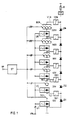
Die Figur 1 zeigt das Blockschaltbild einer beispielhaften Schaltungsanordnung, die aus sechs in Reihe schaltbaren Teilspannungsquellen U1 bis UN (N = 6) besteht. Jede Teilspannungsquelle wir d aus dem Versorgungsnetz VN, z. B. 220 V, 50 Hz, über eine Zweidrahtleitung gespeist und enthält eine Gleichrichteranordnung. Die jeweils erzeugten Gleichspannungen sind ausgehend von einem minimalen Feinstufenwert von z.B. U min = 10 V binär gewichtet und betragen entsprechend der dargestellten Zahlenreihe 10 V bis 320 V. Diese Teilgleichspannungen sind über eine Diodenkaskade D1 bis DN addierbar, so daß an dem Verstärkerausgang eine maximale Gleichspannung von 630 V, in minimalen Stufen von 10 V, erzeugbar ist. Die Verbindungsleitungen VL1 bis VLN zwischen den Teilspannungsquellen U1 bis UN und den zugehörigen Dioden der Diodenkaskade D1 bis DN enthalten jeweils einen Spitzenstrombegrenzer SB1 bis SBN, der im wesentlichen entstehende störende Kommutierungsstromspitzen auf eine nicht störende maximale Stromstärke begrenzt.FIG. 1 shows the block diagram of an exemplary circuit arrangement consisting of six that can be connected in series Partial voltage sources U1 to UN (N = 6) exist. Each partial voltage source is d from the supply network VN, z. B. 220 V, 50 Hz, fed via a two-wire line and contains a rectifier arrangement. The DC voltages generated in each case are binary weighted starting from a minimum fine stage value of, for example, U min = 10 V and, in accordance with the series of numbers shown, are 10 V to 320 V. These partial DC voltages can be added via a diode cascade D1 to DN, so that a maximum DC voltage is present at the amplifier output of 630 V, in minimum steps of 10 V, can be generated. The connecting lines VL1 to VLN between the partial voltage sources U1 to UN and the associated diodes of the diode cascade D1 to DN each contain a peak current limiter SB1 to SBN, which essentially limits disturbing commutation current peaks that arise to a non-disturbing maximum current.
In Fig. 2 ist ein beispielhafter Aufbau einer der Teilspannungsquellen U1 bis UN gezeigt. Die angegebene Schalteranordnung ist eine steuerbare Halbieterschaltung. Als Halbleiter sind z.B. Leistungstransistoren, Feldeffekttransistoren Thyristoren oder GTO's geeignet. Die beispielhaft gewählte Teilspannungsquelle U1 besitzt eine zugehörige Freilaufdiode D1, über die im Falle des gesperrten Halbleiterschalters der Strom des Schaltverstärkers fließt. Wenn sämtliche Teilspannungsquellen U1 bis UN ausgeschaltet sind, fließt kein Strom mehr. Mit NG1 ist ein vorzugsweise dreiphasiger Gleichrichter bezeichnet.2 shows an exemplary structure of one of the partial voltage sources U1 to UN. The switch arrangement specified is a controllable half-turn circuit. For example, power transistors, field-effect transistors, thyristors or GTOs are suitable as semiconductors. The partial voltage source U1 selected as an example has an associated freewheeling diode D1, via which the current of the switching amplifier flows in the case of the blocked semiconductor switch. When all partial voltage sources U1 to UN are switched off, no more current flows. NG1 denotes a preferably three-phase rectifier.
Durch die Spitzenstrombegrenzer SB1 bis SBN (Fig. 1) wird die im wesentlichen durch den Kommutierungsstrom der Freilaufdiode bedingte Stromspitze beim Einschalten der Schalteranordnungen begrenzt, wodurch bedeutend höhere Betriebsströme für die Teilspannungsquellen U1 bis UN möglich sind. Eine solche Einrichtung ist besonders vorteilhaft bei Teilspannungsquellen, die als Schalteranordnung Feldeffekttransistoren benutzen. In Fig. 2 besteht der Spitzenstrombegrenzer SB1 im einfachsten Fall aus einem ohmschen Widerstand. Ein anderes Ausführungsbeispiel für einen Spitzenstrombegrenzer ist eine Parallelschaltung von Widerstand und Spule (Fig. 3), wobei alternativ hierzu in einem oder in beiden Parallelkreisen in Reihe zu Widerstand und Spule noch eine Diode vorgesehen werden kann (Fig. 4).The peak current limiters SB1 to SBN (FIG. 1) limit the current peak which is essentially caused by the commutation current of the freewheeling diode when the switch arrangements are switched on, as a result of which significantly higher operating currents for the partial voltage sources U1 to UN are possible. Such a device is particularly advantageous in the case of partial voltage sources which use field-effect transistors as the switch arrangement. In Fig. 2 the peak current limiter SB1 consists in the simplest case of an ohmic resistor. Another exemplary embodiment of a peak current limiter is a parallel connection of the resistor and the coil (FIG. 3), it being possible as an alternative to provide a diode in one or both parallel circuits in series with the resistor and the coil (FIG. 4).
Der Strombegrenzer ist zwischen dem Ausgang der Schalteranordnung und dem Ausgang der Freilaufdiode angeordnet.The current limiter is arranged between the output of the switch arrangement and the output of the free-wheeling diode.
Bei jeder Teilspannungsquelle U1 bis UN ist jeweils die Gleichrichteranordnung in Reihe geschaltet mit einer Schaltergruppe BG1 bis BGN, so daß die jeweils erzeugte Gleichspannung schaltbar ist. Mindestens eine der Schaltergruppen BG1 bis BGN wird von getrennt steuerbaren, parallel geschalteten Halbleiterschaltern gebildet. Die Anzahl der jeweils parallel zu schaltenden Halbleiterschalter wird aus dem Verhältnis von Schaltfrequenz einer Schaltergruppe zur maximal zulässigen Schaltfrequenz der Halbleiterschalter bestimmt. Die Zahl der parallel geschal teten Halbleiterschalter in den einzelnen Schaltergruppen kann dabei unterschiedlich sein. So könnten z. B. in allen Gruppen mit kleineren binären Spannungswerten, wegen der geringeren Schaltverluste und der Verfügbarkeit schnellerer Halbleiterschalter für kleinere Spannungen, weniger Halbleiterschalter parallel geschaltet werden als bei den Schaltergruppen mit hohen Spannungswerten. Die Steuerung der einzelnen Halbleiterschalter in den verschiedenen Schaltergruppen wird von einer Steuereinheit ST durchgeführt, an deren Eingang das NF-Signal oder ein dementspre chenendes Signal anliegt und von deren Ausgang mehraderige Steuerleitungen zu den Schaltergruppen führen.For each partial voltage source U1 to UN, the rectifier arrangement is connected in series with a switch group BG1 to BGN, so that the DC voltage generated in each case can be switched. At least one of the switch groups BG1 to BGN is formed by separately controllable, parallel-connected semiconductor switches. The number of semiconductor switches to be connected in parallel is determined from the ratio of the switching frequency of a switch group to the maximum permissible switching frequency of the semiconductor switches. The number of semiconductor switches connected in parallel in the individual switch groups can be different. For example, B. in all Groups with smaller binary voltage values, because of the lower switching losses and the availability of faster semiconductor switches for lower voltages, fewer semiconductor switches are connected in parallel than with the switch groups with high voltage values. The control of the individual semiconductor switches in the various switch groups is carried out by a control unit ST, at the input of which the LF signal or a corresponding signal is present and from whose output multi-core control lines lead to the switch groups.
Eine möglichst gleichmäßige zeitliche Verteilung der Verlustleistung der Halbleiterschalter wird dadurch erreicht, daß die parallel geschalteten Halbleiterschalter der Reihe nach ein- und ausgeschaltet werden und die jeweils am längsten nicht beanspruchten Halbleiterschalter der Schaltergruppen wieder zuerst eingeschaltet werden. Damit wird nicht nur eine optimale zeitliche Verteilung der Schaltver luste auf die einzelnen Halbleiterschalter erreicht, sondern gleichzeitig das für Halbleiterschalter in Schaltungsanordnungen mit Freilaufdioden wegen deren hohen Kommutierungsströme nachteilige sofortige Wiedereinschalten eines gerade ausgeschalteten Halbleiterschalters vermieden. A time-uniform distribution of the power loss of the semiconductor switches is achieved in that the semiconductor switches connected in parallel are switched on and off in sequence and the semiconductor switches of the switch groups which have not been used for the longest time are first switched on again. This not only achieves an optimal temporal distribution of the switching losses on the individual semiconductor switches, but at the same time avoids the immediate reclosure of a semiconductor switch that has just been switched off, which is disadvantageous for semiconductor switches in circuit arrangements with free-wheeling diodes because of their high commutation currents.
Claims (4)
- einer ersten Reihenschaltung von mehreren schaltbaren Teilspannungsquellen (U1 bis UN),
- mehreren Freilaufdioden (D1 bis DN), deren Anzahl zumindest derjenigen der Teilspannungsquellen (U1 bis UN) entspricht, in einer zweiten Reihenschaltung, an deren Ausgängen eine Last (R) anschließbar ist,
- mehreren Verbindungsleitungen (VL1 bis VLN), die jeweils einen Verknüpfungspunkt der Teilspannungsquellen (U1 bis UN) mit einem zugehörigen Verknüpfungspunkt der Freilaufdioden (D1 bis DN) verbinden, und
- einer Steuereinheit (ST), welche die Teilspannungsquel len (U1 bis UN) schaltet nach Maßgabe eines zu verstärkenden Niederfrequenz-Signals (NF), das am Eingang der Steuereinheit (ST) anliegt, dadurch gekennzeichnet,
- daß zumindest eine Teilspannungsquelle (U2), die durch das Niederfrequenz-Signal (NF) ansteuerbar ist, durch eine Schaltergruppe (BG2) schaltbar ist,
- daß die Schaltergruppe (BG2)aus mindestens zwei parallel geschalteten Halbleiterschaltern besteht,
- daß die Halbleiterschalter unabhängig voneinander ein- sowie ausschaltbar sind,
- daß für einen ersten Schaltvorgang lediglich eine Teilzahl der Halbleiterschalter benutzt wird und
- daß für einen zeitlich nachfolgenden zweiten Schaltvorgang mindestens ein Halbleiterschalter benutzt wird, der bei dem ersten Schaltvorgang unbenutzt geblieben ist oder lediglich mit einer geringen Verlustleistung beaufschlagt worden ist.1. Fast digital power amplifier, in particular for generating an amplitude-modulated anode voltage for an AM radio transmitter, consisting of
a first series connection of several switchable partial voltage sources (U1 to UN),
several freewheeling diodes (D1 to DN), the number of which corresponds at least to that of the partial voltage sources (U1 to UN), in a second series circuit, at the outputs of which a load (R) can be connected,
- Several connecting lines (VL1 to VLN), each connecting a junction point of the partial voltage sources (U1 to UN) with an associated junction point of the freewheeling diodes (D1 to DN), and
- A control unit (ST), which the partial voltage source len (U1 to UN) switches in accordance with a low-frequency signal (NF) to be amplified, which is present at the input of the control unit (ST), characterized in that
- That at least one partial voltage source (U2), which can be controlled by the low-frequency signal (NF), can be switched by a switch group (BG2),
- That the switch group (BG2) consists of at least two semiconductor switches connected in parallel,
that the semiconductor switches can be switched on and off independently of one another,
- That only a partial number of semiconductor switches is used for a first switching operation and
- That at least one semiconductor switch is used for a temporally subsequent second switching process, which has remained unused in the first switching process or has only been subjected to a low power loss.
Applications Claiming Priority (2)
| Application Number | Priority Date | Filing Date | Title |
|---|---|---|---|
| DE3632716 | 1986-09-26 | ||
| DE19863632716 DE3632716A1 (en) | 1986-09-26 | 1986-09-26 | FAST DIGITAL POWER AMPLIFIER |
Publications (1)
| Publication Number | Publication Date |
|---|---|
| EP0261366A1 true EP0261366A1 (en) | 1988-03-30 |
Family
ID=6310403
Family Applications (1)
| Application Number | Title | Priority Date | Filing Date |
|---|---|---|---|
| EP87111421A Withdrawn EP0261366A1 (en) | 1986-09-26 | 1987-08-07 | Fast digital power amplifier |
Country Status (2)
| Country | Link |
|---|---|
| EP (1) | EP0261366A1 (en) |
| DE (1) | DE3632716A1 (en) |
Cited By (2)
| Publication number | Priority date | Publication date | Assignee | Title |
|---|---|---|---|---|
| EP0349732A1 (en) * | 1988-07-07 | 1990-01-10 | TELEFUNKEN Sendertechnik GmbH | Power amplifier |
| EP0549101A2 (en) * | 1991-11-20 | 1993-06-30 | Continental Electronics Corporation | Amplifier with multiple switched stages and noise suppression |
Families Citing this family (1)
| Publication number | Priority date | Publication date | Assignee | Title |
|---|---|---|---|---|
| DE4135259C1 (en) * | 1991-10-25 | 1993-01-07 | Semikron Elektronik Gmbh, 8500 Nuernberg, De |
Citations (4)
| Publication number | Priority date | Publication date | Assignee | Title |
|---|---|---|---|---|
| EP0058443A1 (en) * | 1981-02-16 | 1982-08-25 | BBC Brown Boveri AG | Method of amplifying an analog low-frequency signal using a switching amplifier and switching amplifier for carrying out said method |
| EP0083727A1 (en) * | 1981-12-24 | 1983-07-20 | Harris Corporation | Amplitude modulator |
| EP0124765A1 (en) * | 1983-05-10 | 1984-11-14 | BBC Brown Boveri AG | Digital power switching amplifier |
| EP0218152A1 (en) * | 1985-09-28 | 1987-04-15 | Licentia Patent-Verwaltungs-GmbH | Switching amplifier |
-
1986
- 1986-09-26 DE DE19863632716 patent/DE3632716A1/en not_active Withdrawn
-
1987
- 1987-08-07 EP EP87111421A patent/EP0261366A1/en not_active Withdrawn
Patent Citations (4)
| Publication number | Priority date | Publication date | Assignee | Title |
|---|---|---|---|---|
| EP0058443A1 (en) * | 1981-02-16 | 1982-08-25 | BBC Brown Boveri AG | Method of amplifying an analog low-frequency signal using a switching amplifier and switching amplifier for carrying out said method |
| EP0083727A1 (en) * | 1981-12-24 | 1983-07-20 | Harris Corporation | Amplitude modulator |
| EP0124765A1 (en) * | 1983-05-10 | 1984-11-14 | BBC Brown Boveri AG | Digital power switching amplifier |
| EP0218152A1 (en) * | 1985-09-28 | 1987-04-15 | Licentia Patent-Verwaltungs-GmbH | Switching amplifier |
Cited By (4)
| Publication number | Priority date | Publication date | Assignee | Title |
|---|---|---|---|---|
| EP0349732A1 (en) * | 1988-07-07 | 1990-01-10 | TELEFUNKEN Sendertechnik GmbH | Power amplifier |
| DE3822990A1 (en) * | 1988-07-07 | 1990-01-11 | Olympia Aeg | POWER AMPLIFIER |
| EP0549101A2 (en) * | 1991-11-20 | 1993-06-30 | Continental Electronics Corporation | Amplifier with multiple switched stages and noise suppression |
| EP0549101A3 (en) * | 1991-11-20 | 1993-09-22 | Continental Electronics Corporation | Amplifier with multiple switched stages and noise suppression |
Also Published As
| Publication number | Publication date |
|---|---|
| DE3632716A1 (en) | 1988-03-31 |
Similar Documents
| Publication | Publication Date | Title |
|---|---|---|
| DE3044956A1 (en) | "DIGITAL HIGH PERFORMANCE AMPLIFIER" | |
| EP0025234B1 (en) | Low frequency power amplifier and its use in an amplitude modulated transmitter | |
| DE2903327C2 (en) | Circuit arrangement for the transmission of direct current signals between galvanically separated signal lines | |
| EP0218152B1 (en) | Switching amplifier | |
| DE3534678A1 (en) | SWITCHING AMPLIFIER | |
| EP0261366A1 (en) | Fast digital power amplifier | |
| DE2854441A1 (en) | DC VOLTAGE REGULATOR | |
| DE2819676A1 (en) | DC voltage converter for power supply - has at least two half-bridge converters using transformer primary winding sections separated by transistors | |
| DE2904231A1 (en) | ELECTRIC AMPLIFIER | |
| EP0267391B1 (en) | Switching amplifier | |
| DE1277356B (en) | Remote DC power supply for telephone amplifiers | |
| EP0048490B1 (en) | Circuit arrangement for transforming a binary input signal into a telegraphy signal | |
| DE3321999C2 (en) | ||
| DE2952654A1 (en) | Push-pull inverter | |
| DE3513239A1 (en) | Circuit network for feeding back circuit energy for semiconductor switches (for example GTO thyristors, power thyristors) | |
| DE2814706C3 (en) | Flyback converter arrangement | |
| DE4042378C2 (en) | ||
| DE929619C (en) | Transistor switching network with number group for message systems | |
| DE1245429B (en) | Amplifier circuit with two transistors, the emitter-collector paths of which are connected in series to the supply voltage | |
| DE60118847T2 (en) | CIRCUIT FOR SIGNAL PROCESSING WITH A CLASS A / B OUTPUT LEVEL FOR CONNECTING TO A SOURCE FOR A VARIETY OF SUPPLY VOLTAGES | |
| DE3430308A1 (en) | Converter | |
| DE2056073A1 (en) | Radio receiver with a switch | |
| DE2043284C3 (en) | Coding translator circuit for use in an adjunct memory system | |
| DE1763778C3 (en) | Electronic multiple remote control system | |
| DE920374C (en) | Diversity recipient |
Legal Events
| Date | Code | Title | Description |
|---|---|---|---|
| PUAI | Public reference made under article 153(3) epc to a published international application that has entered the european phase |
Free format text: ORIGINAL CODE: 0009012 |
|
| AK | Designated contracting states |
Kind code of ref document: A1 Designated state(s): CH DE FR GB LI |
|
| 17P | Request for examination filed |
Effective date: 19880915 |
|
| STAA | Information on the status of an ep patent application or granted ep patent |
Free format text: STATUS: THE APPLICATION IS DEEMED TO BE WITHDRAWN |
|
| 18D | Application deemed to be withdrawn |
Effective date: 19910301 |
|
| RIN1 | Information on inventor provided before grant (corrected) |
Inventor name: LODAHL, MANFRED, DIPL.-ING. |