EP0258951B1 - Process for manufacturing a REFET or a CHEMFET, and the manufactured REFET or CHEMFET - Google Patents
Process for manufacturing a REFET or a CHEMFET, and the manufactured REFET or CHEMFET Download PDFInfo
- Publication number
- EP0258951B1 EP0258951B1 EP87201671A EP87201671A EP0258951B1 EP 0258951 B1 EP0258951 B1 EP 0258951B1 EP 87201671 A EP87201671 A EP 87201671A EP 87201671 A EP87201671 A EP 87201671A EP 0258951 B1 EP0258951 B1 EP 0258951B1
- Authority
- EP
- European Patent Office
- Prior art keywords
- polymer layer
- hydrophilic polymer
- layer
- water
- hydrophilic
- Prior art date
- Legal status (The legal status is an assumption and is not a legal conclusion. Google has not performed a legal analysis and makes no representation as to the accuracy of the status listed.)
- Expired - Lifetime
Links
- 238000000034 method Methods 0.000 title claims abstract description 23
- 238000004519 manufacturing process Methods 0.000 title claims abstract description 12
- 229920001477 hydrophilic polymer Polymers 0.000 claims abstract description 50
- 229920001600 hydrophobic polymer Polymers 0.000 claims abstract description 34
- 239000000463 material Substances 0.000 claims abstract description 18
- XLYOFNOQVPJJNP-UHFFFAOYSA-N water Substances O XLYOFNOQVPJJNP-UHFFFAOYSA-N 0.000 claims abstract description 16
- 239000004065 semiconductor Substances 0.000 claims abstract description 15
- 239000003792 electrolyte Substances 0.000 claims abstract description 7
- 238000010521 absorption reaction Methods 0.000 claims abstract description 3
- 229920000642 polymer Polymers 0.000 claims description 26
- 239000000203 mixture Substances 0.000 claims description 25
- 239000000178 monomer Substances 0.000 claims description 18
- 229920001577 copolymer Polymers 0.000 claims description 15
- 238000006116 polymerization reaction Methods 0.000 claims description 12
- 239000003795 chemical substances by application Substances 0.000 claims description 10
- 150000001875 compounds Chemical class 0.000 claims description 7
- 108010010803 Gelatin Proteins 0.000 claims description 6
- 125000000217 alkyl group Chemical group 0.000 claims description 6
- 125000003118 aryl group Chemical group 0.000 claims description 6
- 229920000159 gelatin Polymers 0.000 claims description 6
- 239000008273 gelatin Substances 0.000 claims description 6
- 235000019322 gelatine Nutrition 0.000 claims description 6
- 235000011852 gelatine desserts Nutrition 0.000 claims description 6
- 150000003961 organosilicon compounds Chemical class 0.000 claims description 6
- 229910052736 halogen Inorganic materials 0.000 claims description 5
- 150000002367 halogens Chemical class 0.000 claims description 5
- 125000000391 vinyl group Chemical group [H]C([*])=C([H])[H] 0.000 claims description 5
- 238000006243 chemical reaction Methods 0.000 claims description 4
- 125000000923 (C1-C30) alkyl group Chemical group 0.000 claims description 2
- 229920001817 Agar Polymers 0.000 claims description 2
- 241000206672 Gelidium Species 0.000 claims description 2
- HTTJABKRGRZYRN-UHFFFAOYSA-N Heparin Chemical compound OC1C(NC(=O)C)C(O)OC(COS(O)(=O)=O)C1OC1C(OS(O)(=O)=O)C(O)C(OC2C(C(OS(O)(=O)=O)C(OC3C(C(O)C(O)C(O3)C(O)=O)OS(O)(=O)=O)C(CO)O2)NS(O)(=O)=O)C(C(O)=O)O1 HTTJABKRGRZYRN-UHFFFAOYSA-N 0.000 claims description 2
- 235000010419 agar Nutrition 0.000 claims description 2
- 125000003545 alkoxy group Chemical group 0.000 claims description 2
- 229920000669 heparin Polymers 0.000 claims description 2
- 229960002897 heparin Drugs 0.000 claims description 2
- 239000000017 hydrogel Substances 0.000 claims description 2
- 125000000951 phenoxy group Chemical group [H]C1=C([H])C([H])=C(O*)C([H])=C1[H] 0.000 claims description 2
- 229920000036 polyvinylpyrrolidone Polymers 0.000 claims description 2
- 235000013855 polyvinylpyrrolidone Nutrition 0.000 claims description 2
- 239000001267 polyvinylpyrrolidone Substances 0.000 claims description 2
- 150000007942 carboxylates Chemical class 0.000 claims 1
- 125000002887 hydroxy group Chemical group [H]O* 0.000 claims 1
- 125000002924 primary amino group Chemical group [H]N([H])* 0.000 claims 1
- VYPSYNLAJGMNEJ-UHFFFAOYSA-N Silicium dioxide Chemical compound O=[Si]=O VYPSYNLAJGMNEJ-UHFFFAOYSA-N 0.000 description 22
- 239000000243 solution Substances 0.000 description 21
- YXFVVABEGXRONW-UHFFFAOYSA-N Toluene Chemical compound CC1=CC=CC=C1 YXFVVABEGXRONW-UHFFFAOYSA-N 0.000 description 12
- 229910052681 coesite Inorganic materials 0.000 description 11
- 229910052906 cristobalite Inorganic materials 0.000 description 11
- 239000000377 silicon dioxide Substances 0.000 description 11
- 235000012239 silicon dioxide Nutrition 0.000 description 11
- 229910052682 stishovite Inorganic materials 0.000 description 11
- 229910052905 tridymite Inorganic materials 0.000 description 11
- 150000002500 ions Chemical class 0.000 description 10
- WYURNTSHIVDZCO-UHFFFAOYSA-N Tetrahydrofuran Chemical compound C1CCOC1 WYURNTSHIVDZCO-UHFFFAOYSA-N 0.000 description 8
- XDLMVUHYZWKMMD-UHFFFAOYSA-N 3-trimethoxysilylpropyl 2-methylprop-2-enoate Chemical compound CO[Si](OC)(OC)CCCOC(=O)C(C)=C XDLMVUHYZWKMMD-UHFFFAOYSA-N 0.000 description 7
- 229920002818 (Hydroxyethyl)methacrylate Polymers 0.000 description 6
- ZWEHNKRNPOVVGH-UHFFFAOYSA-N 2-Butanone Chemical compound CCC(C)=O ZWEHNKRNPOVVGH-UHFFFAOYSA-N 0.000 description 6
- CSCPPACGZOOCGX-UHFFFAOYSA-N Acetone Chemical compound CC(C)=O CSCPPACGZOOCGX-UHFFFAOYSA-N 0.000 description 6
- HEDRZPFGACZZDS-UHFFFAOYSA-N Chloroform Chemical compound ClC(Cl)Cl HEDRZPFGACZZDS-UHFFFAOYSA-N 0.000 description 6
- WOBHKFSMXKNTIM-UHFFFAOYSA-N Hydroxyethyl methacrylate Chemical compound CC(=C)C(=O)OCCO WOBHKFSMXKNTIM-UHFFFAOYSA-N 0.000 description 6
- -1 antibody Proteins 0.000 description 6
- DOIRQSBPFJWKBE-UHFFFAOYSA-N dibutyl phthalate Chemical compound CCCCOC(=O)C1=CC=CC=C1C(=O)OCCCC DOIRQSBPFJWKBE-UHFFFAOYSA-N 0.000 description 6
- 239000005062 Polybutadiene Substances 0.000 description 4
- 229920002857 polybutadiene Polymers 0.000 description 4
- 229920000915 polyvinyl chloride Polymers 0.000 description 4
- 239000004800 polyvinyl chloride Substances 0.000 description 4
- YLQBMQCUIZJEEH-UHFFFAOYSA-N tetrahydrofuran Natural products C=1C=COC=1 YLQBMQCUIZJEEH-UHFFFAOYSA-N 0.000 description 4
- 238000007598 dipping method Methods 0.000 description 3
- 230000002209 hydrophobic effect Effects 0.000 description 3
- 230000035945 sensitivity Effects 0.000 description 3
- 229920002554 vinyl polymer Polymers 0.000 description 3
- MYRTYDVEIRVNKP-UHFFFAOYSA-N 1,2-Divinylbenzene Chemical compound C=CC1=CC=CC=C1C=C MYRTYDVEIRVNKP-UHFFFAOYSA-N 0.000 description 2
- JKNCOURZONDCGV-UHFFFAOYSA-N 2-(dimethylamino)ethyl 2-methylprop-2-enoate Chemical compound CN(C)CCOC(=O)C(C)=C JKNCOURZONDCGV-UHFFFAOYSA-N 0.000 description 2
- NIXOWILDQLNWCW-UHFFFAOYSA-M Acrylate Chemical compound [O-]C(=O)C=C NIXOWILDQLNWCW-UHFFFAOYSA-M 0.000 description 2
- 229910052581 Si3N4 Inorganic materials 0.000 description 2
- PPBRXRYQALVLMV-UHFFFAOYSA-N Styrene Chemical compound C=CC1=CC=CC=C1 PPBRXRYQALVLMV-UHFFFAOYSA-N 0.000 description 2
- GWEVSGVZZGPLCZ-UHFFFAOYSA-N Titan oxide Chemical compound O=[Ti]=O GWEVSGVZZGPLCZ-UHFFFAOYSA-N 0.000 description 2
- XSQUKJJJFZCRTK-UHFFFAOYSA-N Urea Chemical compound NC(N)=O XSQUKJJJFZCRTK-UHFFFAOYSA-N 0.000 description 2
- MCMNRKCIXSYSNV-UHFFFAOYSA-N Zirconium dioxide Chemical compound O=[Zr]=O MCMNRKCIXSYSNV-UHFFFAOYSA-N 0.000 description 2
- 150000001450 anions Chemical class 0.000 description 2
- 239000000427 antigen Substances 0.000 description 2
- 102000036639 antigens Human genes 0.000 description 2
- 108091007433 antigens Proteins 0.000 description 2
- 239000004202 carbamide Substances 0.000 description 2
- 150000001768 cations Chemical class 0.000 description 2
- 239000003153 chemical reaction reagent Substances 0.000 description 2
- 239000003431 cross linking reagent Substances 0.000 description 2
- 230000000694 effects Effects 0.000 description 2
- 238000005516 engineering process Methods 0.000 description 2
- 238000005259 measurement Methods 0.000 description 2
- 230000035515 penetration Effects 0.000 description 2
- 229920002635 polyurethane Polymers 0.000 description 2
- 108090000623 proteins and genes Proteins 0.000 description 2
- 102000004169 proteins and genes Human genes 0.000 description 2
- 238000010992 reflux Methods 0.000 description 2
- 239000000126 substance Substances 0.000 description 2
- 238000005406 washing Methods 0.000 description 2
- KWVGIHKZDCUPEU-UHFFFAOYSA-N 2,2-dimethoxy-2-phenylacetophenone Chemical compound C=1C=CC=CC=1C(OC)(OC)C(=O)C1=CC=CC=C1 KWVGIHKZDCUPEU-UHFFFAOYSA-N 0.000 description 1
- SBYMUDUGTIKLCR-UHFFFAOYSA-N 2-chloroethenylbenzene Chemical compound ClC=CC1=CC=CC=C1 SBYMUDUGTIKLCR-UHFFFAOYSA-N 0.000 description 1
- FCYVWWWTHPPJII-UHFFFAOYSA-N 2-methylidenepropanedinitrile Chemical compound N#CC(=C)C#N FCYVWWWTHPPJII-UHFFFAOYSA-N 0.000 description 1
- WMBFARVSOWVDII-UHFFFAOYSA-N 20-ethenyl-2,5,8,11,14,17-hexaoxabicyclo[16.4.0]docosa-1(18),19,21-triene Chemical compound O1CCOCCOCCOCCOCCOC2=CC(C=C)=CC=C21 WMBFARVSOWVDII-UHFFFAOYSA-N 0.000 description 1
- IWTYTFSSTWXZFU-UHFFFAOYSA-N 3-chloroprop-1-enylbenzene Chemical compound ClCC=CC1=CC=CC=C1 IWTYTFSSTWXZFU-UHFFFAOYSA-N 0.000 description 1
- NLHHRLWOUZZQLW-UHFFFAOYSA-N Acrylonitrile Chemical compound C=CC#N NLHHRLWOUZZQLW-UHFFFAOYSA-N 0.000 description 1
- WQZGKKKJIJFFOK-GASJEMHNSA-N Glucose Natural products OC[C@H]1OC(O)[C@H](O)[C@@H](O)[C@@H]1O WQZGKKKJIJFFOK-GASJEMHNSA-N 0.000 description 1
- 239000007836 KH2PO4 Substances 0.000 description 1
- WHNWPMSKXPGLAX-UHFFFAOYSA-N N-Vinyl-2-pyrrolidone Chemical compound C=CN1CCCC1=O WHNWPMSKXPGLAX-UHFFFAOYSA-N 0.000 description 1
- 241000047703 Nonion Species 0.000 description 1
- 229920012485 Plasticized Polyvinyl chloride Polymers 0.000 description 1
- BLRPTPMANUNPDV-UHFFFAOYSA-N Silane Chemical compound [SiH4] BLRPTPMANUNPDV-UHFFFAOYSA-N 0.000 description 1
- XTXRWKRVRITETP-UHFFFAOYSA-N Vinyl acetate Chemical compound CC(=O)OC=C XTXRWKRVRITETP-UHFFFAOYSA-N 0.000 description 1
- 230000002378 acidificating effect Effects 0.000 description 1
- PNEYBMLMFCGWSK-UHFFFAOYSA-N aluminium oxide Inorganic materials [O-2].[O-2].[O-2].[Al+3].[Al+3] PNEYBMLMFCGWSK-UHFFFAOYSA-N 0.000 description 1
- 125000003277 amino group Chemical group 0.000 description 1
- 238000004458 analytical method Methods 0.000 description 1
- 239000003242 anti bacterial agent Substances 0.000 description 1
- 239000012298 atmosphere Substances 0.000 description 1
- WQZGKKKJIJFFOK-VFUOTHLCSA-N beta-D-glucose Chemical compound OC[C@H]1O[C@@H](O)[C@H](O)[C@@H](O)[C@@H]1O WQZGKKKJIJFFOK-VFUOTHLCSA-N 0.000 description 1
- 230000003115 biocidal effect Effects 0.000 description 1
- 239000008366 buffered solution Substances 0.000 description 1
- 125000000484 butyl group Chemical group [H]C([*])([H])C([H])([H])C([H])([H])C([H])([H])[H] 0.000 description 1
- 229910052593 corundum Inorganic materials 0.000 description 1
- 150000003983 crown ethers Chemical class 0.000 description 1
- 230000001419 dependent effect Effects 0.000 description 1
- KPUWHANPEXNPJT-UHFFFAOYSA-N disiloxane Chemical class [SiH3]O[SiH3] KPUWHANPEXNPJT-UHFFFAOYSA-N 0.000 description 1
- BNIILDVGGAEEIG-UHFFFAOYSA-L disodium hydrogen phosphate Chemical compound [Na+].[Na+].OP([O-])([O-])=O BNIILDVGGAEEIG-UHFFFAOYSA-L 0.000 description 1
- 229910000397 disodium phosphate Inorganic materials 0.000 description 1
- 235000019800 disodium phosphate Nutrition 0.000 description 1
- 229920001971 elastomer Polymers 0.000 description 1
- 238000000572 ellipsometry Methods 0.000 description 1
- JROGBPMEKVAPEH-GXGBFOEMSA-N emetine dihydrochloride Chemical compound Cl.Cl.N1CCC2=CC(OC)=C(OC)C=C2[C@H]1C[C@H]1C[C@H]2C3=CC(OC)=C(OC)C=C3CCN2C[C@@H]1CC JROGBPMEKVAPEH-GXGBFOEMSA-N 0.000 description 1
- 238000001704 evaporation Methods 0.000 description 1
- 230000008020 evaporation Effects 0.000 description 1
- 230000002349 favourable effect Effects 0.000 description 1
- 230000005669 field effect Effects 0.000 description 1
- 125000000524 functional group Chemical group 0.000 description 1
- 239000007789 gas Substances 0.000 description 1
- 239000008103 glucose Substances 0.000 description 1
- 239000005556 hormone Substances 0.000 description 1
- 229940088597 hormone Drugs 0.000 description 1
- 125000004356 hydroxy functional group Chemical group O* 0.000 description 1
- 238000007654 immersion Methods 0.000 description 1
- 238000010348 incorporation Methods 0.000 description 1
- 239000003999 initiator Substances 0.000 description 1
- 125000002496 methyl group Chemical group [H]C([H])([H])* 0.000 description 1
- SNVLJLYUUXKWOJ-UHFFFAOYSA-N methylidenecarbene Chemical group C=[C] SNVLJLYUUXKWOJ-UHFFFAOYSA-N 0.000 description 1
- 229910000402 monopotassium phosphate Inorganic materials 0.000 description 1
- 235000019796 monopotassium phosphate Nutrition 0.000 description 1
- 239000012299 nitrogen atmosphere Substances 0.000 description 1
- 229920000191 poly(N-vinyl pyrrolidone) Polymers 0.000 description 1
- 239000004814 polyurethane Substances 0.000 description 1
- GNSKLFRGEWLPPA-UHFFFAOYSA-M potassium dihydrogen phosphate Chemical compound [K+].OP(O)([O-])=O GNSKLFRGEWLPPA-UHFFFAOYSA-M 0.000 description 1
- 230000009257 reactivity Effects 0.000 description 1
- 239000005060 rubber Substances 0.000 description 1
- 229910000077 silane Inorganic materials 0.000 description 1
- 125000005372 silanol group Chemical group 0.000 description 1
- 238000004528 spin coating Methods 0.000 description 1
- 239000000758 substrate Substances 0.000 description 1
- PBCFLUZVCVVTBY-UHFFFAOYSA-N tantalum pentoxide Inorganic materials O=[Ta](=O)O[Ta](=O)=O PBCFLUZVCVVTBY-UHFFFAOYSA-N 0.000 description 1
- UKRDPEFKFJNXQM-UHFFFAOYSA-N vinylsilane Chemical class [SiH3]C=C UKRDPEFKFJNXQM-UHFFFAOYSA-N 0.000 description 1
- 229910001845 yogo sapphire Inorganic materials 0.000 description 1
Classifications
-
- G—PHYSICS
- G01—MEASURING; TESTING
- G01N—INVESTIGATING OR ANALYSING MATERIALS BY DETERMINING THEIR CHEMICAL OR PHYSICAL PROPERTIES
- G01N27/00—Investigating or analysing materials by the use of electric, electrochemical, or magnetic means
- G01N27/26—Investigating or analysing materials by the use of electric, electrochemical, or magnetic means by investigating electrochemical variables; by using electrolysis or electrophoresis
- G01N27/403—Cells and electrode assemblies
- G01N27/414—Ion-sensitive or chemical field-effect transistors, i.e. ISFETS or CHEMFETS
Definitions
- the current invention relates to the manufacture of a REFET when an ISFET is coated with an inert hydrophobic layer, or of a CHEMFET, when an ISFET is modified with a hydrophobic layer, which contains a receptor molecule for a chemical compound to be measured, for example a cation, anion, proton, urea, sugar, protein, antibody, antigen.
- ISFET Ion Sensitive Field Effect Transistor
- ISFET is understood a semiconductor material provided with an isolator layer.
- the ISFETs are made in accordance with standard MOS technology.
- the isolator layer is thermally deposited at 1150° C for 15 min. in an O2 atmosphere. The layer thickness amounts to ca. 700 ⁇ .
- REFET and CHEMFET possess a number of advantages:
- the isolator layer (usually designated as gate-oxide layer) applied to the semiconductor material can for example consist either of layers of SiO2, Al2O3, Ta2O5, TiO2, ZrO2 and/or Si3N4 (not an oxide!) or of a layered structure consisting of materials differing from one another.
- the exterior surface of the isolator layer contains chemically reactive, particularly protonic groups (silanol groups in the case of SiO2 and amine groups in the case of Si3N4). These groups ensure that the chemically non-modified ISFET gives response to the changes in the proton concentration. It is desirable for the measurement of other chemical compounds to take steps in order to suppress or entirely eliminate this proton sensitivity. These steps can consist of allowing these reactive groups to react, as a result of which the reactivity disappears, of covering the isolator layer with an inert, hydrophobic polymer, or of covalent bonding of an inert, hydrophobic polymer to the isolator layer. This latter possibility is comprehensively described in the international patent application WO 85/04480 in the name of applicant, the Stichting Centrum voor Micro-Electronica Twente of Enschede.
- hydrophobic polymer contains ionophors a specific ion sensitivity and ion specificity occurs that is specifically dependent upon the ionophors.
- ISFET an ISFET
- REFET An H+ insensitive ISFET
- a process for manufacturing such a FET comprises: a) covalent bonding of a hydrophilic polymer layer to an isolator layer applied to a semiconductor material; b) the absorption of water or a watery solution into the hydrophilic polymer layer; and c) the binding of a hydrophobic polymer layer to the water-holding hydrophilic polymer layer. Reproducibility will moreover improve during production.
- the hydrophilic polymer layer should be covalently bonded to the isolator layer since otherwise a durability is achieved amounting only to several hours, which is unsuitable for practical use.
- the hydrophilic polymer layer preferably also contains an electrolyte so that the fall in potential over the interface between the hydrophilic polymer layer and the hydrophobic polymer layer is determined and is virtually independent of the composition of the solution for measuring.
- an ion to be measured with the CHEMFET preferably forms part of the electrolyte.
- the hydrophilic polymer layer also contains a buffer.
- the pH in the hydrophilic polymer layer is kept substantially constant, also when there is penetration of H+ ions or penetration of CO2 through the hydrophobic polymer layer.
- a particularly favourable CHEMFET or REFET is obtained if the hydrophilic polymer layer contains an electrolyte as well as a buffer.
- the hydrophilic polymer layer has a thickness of 0.0050-200 ⁇ m, and preferably of 0.1-100 ⁇ m, and more preferably 1-50 ⁇ m.
- a bi-functional organosilicon compound which contains on the one hand a group which can be covalently bonded with the isolator layer and on the other a group to which can be covalently bonded either monomers which are to be made to react to form polymers or polymerized material.
- Organosilylation reagents used are mentioned in (P. Bergveld, N.F. de Kooy, Ned. Tijdschr. v. Natuur ambience (Dutch Journal of Physics), A46 , 22-25 (1980)). Particularly applicable are the organosilicon compounds I and II from table 1.
- the hydrophilic polymer layer can be formed by polymerization of monomers geared to the covalently bonded, bi-functional organosilicon compound. Photochemically polymerizable monomers are for instance used in order to enable IC compatible mass production.
- the hydrophilic polymer layer can be formed by polymerization and comprises
- Copolymers of the above mentioned monomers can also be formed with vinyl silanes (Table 1). These materials can be directly linked covalently to the isolator layer.
- hydrophilic polymer layer is applied to the isolator layer.
- Water or a watery solution is then allowed to penetrate into the hydrophilic layer by means of immersion or addition of a required amount of water.
- hydrophobic polymer layer is applied over the hydrophilic polymer layer which now contains water.
- the binding can be performed physically or covalently (chemically).
- the hydrophobic polymer layer is formed by polymerization of monomers containing vinyl groups or by a reaction with "living" polymers.
- linking agent is necessary if, when a covalent bonding is required, it is not possible to make the hydrophobic layer react covalently with functional groups of the hydrophilic polymer layer that are present.
- silylating reagents as linking agent.
- silylating reagents See: Deschler,U., Kleinschmit,P., Panster,P.; Angew. Chemie, 98 , 237-253, (1986)).
- polymers that are provided with reactive silane monomers.
- hydrophobic polymer layer physically to the hydrophilic polymer layer. This physical binding is realized with the previously described polymers but with omission of the linking agent.
- Plasticized PVC, siloxane rubbers and polybutadiene can also be used as polymer.
- REFET a sensor in which such a FET is included will act as a so-called REFET.
- This REFET gives a non-ion specific response to variation in the total ion concentration. When the ion strength in the solution to be measured is constant, it therefore acts as a pseudo-reference electrode.
- a receptor is incorporated in the hydrophobic polymer layer, a sensor equipped with same acts as a CHEMFET.
- the receptor can be bonded covalently or physically into the hydrophobic polymer layer, or entangled therein during polymerization.
- the receptor can be an ionophor, such as an antibiotic (e.g. valinomycine), a crown ether, cryptate, podand, hemispherand, cryptohemispherand, spherand.
- an antibiotic e.g. valinomycine
- a crown ether e.g. a benzyl ether
- cryptate e.g. a benzyl ether
- podand e.g. hemispherand
- cryptohemispherand spherand.
- An H+ sensitive CHEMFET is manufactured by incorporating as ionophor in the inert hydrophobic polymer layer a compound with acidic or basic groups, for instance tridodecyclamine.
- thermodynamic activity of cations as well as anions can of course be determined.
- a plaque of semiconductor material for treatment which is provided with an isolator layer consisting of SiO2. After washing with methylethylketone the plaque is dried for 1 hour at 80°C. Hydroxyethylmethacrylate (HEMA; Janssen, Belgium) is then applied in accordance with the so-called dipping method. Polymerization and covalent bonding to the isolator layer are performed photochemically.
- HEMA Hydroxyethylmethacrylate
- the thickness of the hydrophilic polymer layer amounts to 15 ⁇ m and is determined in accordance with ellipsometry.
- the covalently bonded hydrophilic polymer layer is swelled for 30 mins. at room temperature with a solution of 0.1 M KCl + 0.025 M KH2PO4 + 0.025 M Na2HPO4 in water.
- a polybutadiene solution (mol.wt. 4300, 99% unsaturated, 25% vinyl and 40% trans-1,4, obtainable from Janssen, Belgium) in tetrahydrofuran is subsequently applied to the water holding, hydrophilic polymer layer and then polymerized photochemically.
- the thickness of the hydrophobic polymer layer covalently bonded to the hydrophilic, water-holding polymer layer is 10 ⁇ m.
- a hydrophilic polymer layer is applied to the isolator layer.
- the outer side of the hydrophilic polymer is then functionalized by reaction with methacryl oxychloride. In this way a part of the hydroxyethyl groups are converted into methacryloxy groups and the hydrophilic polymer layer is swelled in the watery, buffered KCl solution, as described in example 1.
- the layer thickness of the hydrophobic polymer layer is 15 ⁇ m and it is cross linked with the applied methacryloxy functional groups.
- hydrophilic polymer layer is applied covalently to the isolator layer and swelled in the watery, buffered KCl solution, as described in example 1.
- a solution of polyvinylchloride (PVC, obtainable from Fluka, Switzerland, purum; for ion selective electrodes 30% by weight), di-n-butyl phthalate (67% by weight) and valinomycine (obtainable from Fluka, Switzerland, purum pro analysis; 3% by weight) in tetrahydrofuran is then applied.
- the formed hydrophobic polymer layer has a thickness of 10 ⁇ m.
- a plaque of semiconductor material for treatment which is provided with an isolator layer consisting of SiO2. After thorough washing with methylethylketone the plaque is dried for 1 hour at 80°C. This plaque is then placed in a solution of polybutadiene (mol.wt. 3400, 99% unsaturated, 25% vinyl and 40% trans-1,4, obtainable from Janssen, Belgium) in tetrahydrofuran. Photochemical polymerization then takes place. The thickness of the hydrophobic polymer layer covalently applied directly onto the isolator layer is 10 ⁇ m.
- the thickness of the hydrophobic polymer layer covalently bonded directly onto the isolator layer is 15 ⁇ m.
- a physically bonded hydrophobic polymer layer is bonded directly onto a plaque of semiconductor material that is provided with an isolator layer of SiO2.
- a solution of polyvinylchloride (30% by weight), di-n-butyl phthalate (67% by weight) and valinomycine (3% by weight) is placed in tetrahydrofuran.
- the layer thickness of this physically bonded hydrophobic polymer layer provided with a receptor is 10 ⁇ m.
- ACE + Epocryl 40:60 w/w
- chloroform which is photochemically polymerized as previously described.
- the layer thickness of the hydrophobic polymer layer is 15 ⁇ m.
- a mixture of 3 parts by wt. methacryloxypropyltrimethoxysilane and 7 parts by wt. hydroxyethyl methacrylate (HEMA) in toluene is photochemically polymerized.
- the toluene is distilled off and the product is dissolved in acetone.
- Applied to the plaque of semiconductor material for treatment that is provided with an isolator layer consisting of SiO2 is a part of the prepared polymer solution in acetone. After evaporation of the acetone the semiconductor material is placed in an oven for 24 hours at 80°C.
- the thus covalently bonded hydrophilic polymer layer has a thickness of 20 ⁇ m.
- the watery, buffered KCl solution, as described in example 1, is then absorbed by this polymer.
- a mixture of ACE and Epocryl is then applied, as according to example 2, to this swelled polymer layer and polymerized.
- the layer thickness amounts to 15 ⁇ m.
- the buffered, watery KCl solution is then absorbed by this polymer.
- a hydrophobic polymer layer consisting of PVC, di-n-butyl phthalate and valinomycine is then applied.
- the formed layer has a thickness of 10 ⁇ m.
- a hydrophilic polymer layer is applied to the isolator layer and swelled in the watery, buffered KCl solution, also as described in example 1.
- Onto the hydrophilic, water-holding polymer layer is then applied and cross linked a mixture of Silopren K 1000 (85% by wt.) cross-linking agent KA-1 (12% by wt.; both from Bayer AG, Leverkusen, Germany) and valinomycine (3% by wt.).
- the layer thickness amounts to 15 ⁇ m.
- silylating process is performed.
- a mixture of Silopren K 1000 (85% by wt.) cross-linking agent KA-1 (12% by wt.) and valinomycine (3% by wt.) is then applied and cross linked.
- the layer thickness amounts to 15 ⁇ m.
- a plaque of semiconductor material provided with an isolator layer consisting of SiO2 is, as described in example 1, silylated with methacryloxypropyltrimeth oxysilane. Subsequently a mixture of hydroxyethylmethacrylate (60 pts.by wt.) and N-vinyl-2-pyrrolidone (40 pts.by wt.; Janssen, Belgium) is applied in accordance with the dipping method. Polymerization and covalent binding to the isolator layer is performed photochemically. The thickness of the hydrophilic polymer layer amounts to 20 ⁇ m. As is described in example 1, the watery, buffered KCl solution is then absorbed by this polymer. A mixture of ACE and Epocryl is then applied, as in example 2, to this swelled polymer layer and photochemically polymerized. The layer thickness amounts to 15 ⁇ m.
- a plaque of semiconductor material provided with an isolator layer consisting of SiO2 is, as described in example 1, silylated with methacryloxypropyltrimeth oxysilane. Subsequently N,N-dimethylaminoethylmethacrylate (DMAEMA, Janssen Belgium) is applied in accordance with the dipping method. Polymerization and covalent binding is performed photochemically. The thickness of the hydrophilic polymer layer amounts to 25 ⁇ m. As is described in example 1, a watery, buffered KCl solution is then absorbed by this polymer. A mixture of ACE and Epocryl is then applied, as in example 2, to this swelled polymer layer and photochemically polymerized. The layer thickness amounts to 15 ⁇ m.
- a plaque of semiconductor material provided with an isolator layer consisting of SiO2 is, as described in example 1, silylated with methacryloxypropyltrimeth oxysilane.
- a hydrophilic polymer layer is then applied which is subsequently functionalized by reaction with methacryl oxychloride, the watery, buffered solution then being absorbed as described in example 1.
- Onto the hydrophilic polymer layer is then applied a mixture of polybutadiene (for details see example 1) and 4 -vinylbenzo-18-crown-6 (5% by wt.) and polymerized photochemically. Layer thickness 10 ⁇ m.
- the modified REFETs and CHEMFETs were measured in accordance with the procedure as described by A.van den Berg, P. Bergveld, D.N. Reinhoudt and E.J.R. Sudhölter, Sensors and Actuators 8 129-148 (1985).
- a sensor furnished with a REFET such as that of example 7 gave during measurement at pH 7 a continuous increase in the response. After being exposed to this solution for 5 hours a pH response was observed which corresponded to a non-modified ISFET.
- a sensor containing a REFET as manufactured in example 2 was found after spending a month in a solution at pH 7 to still display the original, even pH response.
Landscapes
- Life Sciences & Earth Sciences (AREA)
- Chemical & Material Sciences (AREA)
- Health & Medical Sciences (AREA)
- Biochemistry (AREA)
- General Physics & Mathematics (AREA)
- Microelectronics & Electronic Packaging (AREA)
- Chemical Kinetics & Catalysis (AREA)
- Electrochemistry (AREA)
- Physics & Mathematics (AREA)
- Analytical Chemistry (AREA)
- Engineering & Computer Science (AREA)
- General Health & Medical Sciences (AREA)
- Molecular Biology (AREA)
- Immunology (AREA)
- Pathology (AREA)
- Organic Low-Molecular-Weight Compounds And Preparation Thereof (AREA)
- Compositions Of Macromolecular Compounds (AREA)
- Laminated Bodies (AREA)
- Investigating Or Analyzing Materials By The Use Of Electric Means (AREA)
- Addition Polymer Or Copolymer, Post-Treatments, Or Chemical Modifications (AREA)
- Silicon Polymers (AREA)
Abstract
Description
- The current invention relates to the manufacture of a REFET when an ISFET is coated with an inert hydrophobic layer, or of a CHEMFET, when an ISFET is modified with a hydrophobic layer, which contains a receptor molecule for a chemical compound to be measured, for example a cation, anion, proton, urea, sugar, protein, antibody, antigen. By ISFET (Ion Sensitive Field Effect Transistor) is understood a semiconductor material provided with an isolator layer. The ISFETs are made in accordance with standard MOS technology. The isolator layer is thermally deposited at 1150° C for 15 min. in an O₂ atmosphere. The layer thickness amounts to ca. 700 Å.
- Compared to the conventional ion selective electrodes, REFET and CHEMFET possess a number of advantages:
- 1) they are small and therefore possibly suitable for biomedical applications;
- 2) they are robust;
- 3) they can be manufactured using IC technology, thereby enabling the manufacture of a miniature multi-sensor;
- 4) mass production at low cost is possible without problem;
- 5) as a result of the low output impedance the sensitivity to external interference signals is smaller; and
- 6) they possess a better signal-to-noise ratio.
- The isolator layer (usually designated as gate-oxide layer) applied to the semiconductor material can for example consist either of layers of SiO₂, Al₂O₃, Ta₂O₅, TiO₂, ZrO₂ and/or Si₃N₄ (not an oxide!) or of a layered structure consisting of materials differing from one another.
- The exterior surface of the isolator layer contains chemically reactive, particularly protonic groups (silanol groups in the case of SiO₂ and amine groups in the case of Si₃N₄). These groups ensure that the chemically non-modified ISFET gives response to the changes in the proton concentration. It is desirable for the measurement of other chemical compounds to take steps in order to suppress or entirely eliminate this proton sensitivity. These steps can consist of allowing these reactive groups to react, as a result of which the reactivity disappears, of covering the isolator layer with an inert, hydrophobic polymer, or of covalent bonding of an inert, hydrophobic polymer to the isolator layer. This latter possibility is comprehensively described in the international patent application WO 85/04480 in the name of applicant, the Stichting Centrum voor Micro-Electronica Twente of Enschede.
- If the hydrophobic polymer contains ionophors a specific ion sensitivity and ion specificity occurs that is specifically dependent upon the ionophors. Such an ISFET is called a CHEMFET. An H⁺ insensitive ISFET is called a REFET.
- After extensive research it has been found that the characteristics of a sensor containing such a REFET and/or CHEMFET as an essential component can be markedly improved in respect of noise, drift and hysteresis. This is achieved according to the invention when a process for manufacturing such a FET comprises: a) covalent bonding of a hydrophilic polymer layer to an isolator layer applied to a semiconductor material; b) the absorption of water or a watery solution into the hydrophilic polymer layer; and c) the binding of a hydrophobic polymer layer to the water-holding hydrophilic polymer layer. Reproducibility will moreover improve during production.
- It was found during this research that many problems relating to the characteristics referred to above could be traced back to unverifiable variations in the chemical structure at the location of the interface between the isolator layer and the hydrophobic polymer layer applied thereto. These variations were inherent to the conventional fabrication methods employed.
- Application of the water-holding, hydrophilic polymer layer between the isolator layer and the hydrophobic polymer layer results in thermodynamically and chemically better defined interfaces between on the one hand isolator layer and hydrophilic polymer layer and on the other between the hydrophilic polymer layer and the hydrophobic polymer layer.
- The hydrophilic polymer layer should be covalently bonded to the isolator layer since otherwise a durability is achieved amounting only to several hours, which is unsuitable for practical use.
- The hydrophilic polymer layer preferably also contains an electrolyte so that the fall in potential over the interface between the hydrophilic polymer layer and the hydrophobic polymer layer is determined and is virtually independent of the composition of the solution for measuring. In the case of a CHEMFET an ion to be measured with the CHEMFET preferably forms part of the electrolyte.
- It is further to be recommended that the hydrophilic polymer layer also contains a buffer. In this way the pH in the hydrophilic polymer layer is kept substantially constant, also when there is penetration of H⁺ ions or penetration of CO₂ through the hydrophobic polymer layer. A particularly favourable CHEMFET or REFET is obtained if the hydrophilic polymer layer contains an electrolyte as well as a buffer.
- The hydrophilic polymer layer has a thickness of 0.0050-200 µm, and preferably of 0.1-100 µm, and more preferably 1-50 µm.
- Various possibilities are available for the manufacture of a hydrophilic polymer layer covalently bonded to the isolator layer.
- For the covalent linking it is possible on the one hand to use a bi-functional organosilicon compound which contains on the one hand a group which can be covalently bonded with the isolator layer and on the other a group to which can be covalently bonded either monomers which are to be made to react to form polymers or polymerized material.
- Organosilylation reagents used are mentioned in (P. Bergveld, N.F. de Kooy, Ned. Tijdschr. v. Natuurkunde (Dutch Journal of Physics), A46, 22-25 (1980)). Particularly applicable are the organosilicon compounds I and II from table 1.
- After the bi-functional organosilicon compound has been covalently bonded to the isolator layer, the hydrophilic polymer layer can be formed by polymerization of monomers geared to the covalently bonded, bi-functional organosilicon compound. Photochemically polymerizable monomers are for instance used in order to enable IC compatible mass production. In the case of the compounds I and II the hydrophilic polymer layer can be formed by polymerization and comprises
- a) monomers with the structure formulae:

- R⁴:
- -H -R⁵-OH R⁵-NH₂ R⁵-SH R⁵-N(CH₃)₂ R⁵-sugar R⁵-peptide
- R⁵:
- alkyl, aryl
- B :
- OH, NH₂,

- b) copolymers with additional monomers having the structure formula III, in which R₄ is now a C₁-C₃₀ alkyl group,
- c) mixtures of (co)polymers with a hydrogel, such as gelatin, agar-agar, heparin and polyvinyl pyrrolidone,
- d) copolymers of the monomers III an IV,
- e) mixtures of polymers and/or copolymers of the monomers III and IV,
- f) mixtures of (co)polymers of the monomers III and/or IV with the copolymers as according to point b,
- g) mixtures of the polymers and/or copolymers named under points a-f.
- Copolymers of the above mentioned monomers can also be formed with vinyl silanes (Table 1). These materials can be directly linked covalently to the isolator layer.
- In this way the hydrophilic polymer layer is applied to the isolator layer.
- Water or a watery solution is then allowed to penetrate into the hydrophilic layer by means of immersion or addition of a required amount of water.
- Finally, the hydrophobic polymer layer is applied over the hydrophilic polymer layer which now contains water. The binding can be performed physically or covalently (chemically).
- In the case of a covalent bonding use can be made of a linking agent with the structure formula:

in which R³ has the denotation stated above, and
Z = halogen, alkoxy, phenoxy or hydroxy. - The hydrophobic polymer layer is formed by polymerization of monomers containing vinyl groups or by a reaction with "living" polymers.
- The use of a linking agent is necessary if, when a covalent bonding is required, it is not possible to make the hydrophobic layer react covalently with functional groups of the hydrophilic polymer layer that are present.
- In the case of the above mentioned linking agent, use can then be made of monomers containing vinyls, as referred to in WO 85/04480, and in addition styrene, divinyl benzene, acrylonitrile, vinyl acetate, methyl(meth)acrylate, butyl(meth)acrylate, vinylidene cyanide, chlorostyrene and for example chloromethyl styrene.
- It is of course also possible to use silylating reagents as linking agent. (See: Deschler,U., Kleinschmit,P., Panster,P.; Angew. Chemie, 98, 237-253, (1986)). In addition it is also possible to make use of polymers that are provided with reactive silane monomers.
- In the case of application of a polymer layer consisting of polyurethanes or polycarbamates or other polymers which are reactive with respect to the hydrophilic layer, it is not necessary to make use of the linking agent.
- It is further possible to adhere the hydrophobic polymer layer physically to the hydrophilic polymer layer. this physical binding is realized with the previously described polymers but with omission of the linking agent. Plasticized PVC, siloxane rubbers and polybutadiene can also be used as polymer.
- Finally, it is likewise possible to employ so-called "living" polymers.
- If no receptor is incorporated in the inert hydrophobic polymer layer, a sensor in which such a FET is included will act as a so-called REFET. This REFET gives a non-ion specific response to variation in the total ion concentration. When the ion strength in the solution to be measured is constant, it therefore acts as a pseudo-reference electrode.
- If a receptor is incorporated in the hydrophobic polymer layer, a sensor equipped with same acts as a CHEMFET. The receptor can be bonded covalently or physically into the hydrophobic polymer layer, or entangled therein during polymerization.
- The receptor can be an ionophor, such as an antibiotic (e.g. valinomycine), a crown ether, cryptate, podand, hemispherand, cryptohemispherand, spherand.
- An H⁺ sensitive CHEMFET is manufactured by incorporating as ionophor in the inert hydrophobic polymer layer a compound with acidic or basic groups, for instance tridodecyclamine.
- As a result of the choice of a specific receptor and its incorporation in the hydrophobic polymer layer, it is possible to measure selectively the presence and the (thermodynamic) activity in solutions of chemical, and particularly biochemical, compounds such as ions, proteins, substrates, antibodies antigens, hormones, gases, glucose, urea and the like.
- Stressed is the fact that the thermodynamic activity of cations as well as anions can of course be determined.
- The current invention will be elucidated with reference to a number of examples according to the invention and reference examples, although the invention is in no way limited thereto.
- Placed for two hours in a mixture of methacryloxypropyltrimeth oxysilane (Alfa, US) and toluene which is boiled under reflux conditions is a plaque of semiconductor material for treatment which is provided with an isolator layer consisting of SiO₂. After washing with methylethylketone the plaque is dried for 1 hour at 80°C. Hydroxyethylmethacrylate (HEMA; Janssen, Belgium) is then applied in accordance with the so-called dipping method. Polymerization and covalent bonding to the isolator layer are performed photochemically. The polymerization reactions are initiated, using the photo-initiator 2,2-dimethoxy-2-phenylacetophenon (4% by weight; Janssen, Belgium) which is present in the mixture to be polymerized, by radiating the mixture with an ultraviolet source (λmax = 360 nm) for 2-10 mins. under an N₂ atmosphere.
- The thickness of the hydrophilic polymer layer amounts to 15 µm and is determined in accordance with ellipsometry.
- The covalently bonded hydrophilic polymer layer is swelled for 30 mins. at room temperature with a solution of 0.1 M KCl + 0.025 M KH₂PO₄ + 0.025 M Na₂HPO₄ in water.
- A polybutadiene solution (mol.wt. 4300, 99% unsaturated, 25% vinyl and 40% trans-1,4, obtainable from Janssen, Belgium) in tetrahydrofuran is subsequently applied to the water holding, hydrophilic polymer layer and then polymerized photochemically. The thickness of the hydrophobic polymer layer covalently bonded to the hydrophilic, water-holding polymer layer is 10 µm.
- In a manner similar to that described in example 1 a hydrophilic polymer layer is applied to the isolator layer. The outer side of the hydrophilic polymer is then functionalized by reaction with methacryl oxychloride. In this way a part of the hydroxyethyl groups are converted into methacryloxy groups and the hydrophilic polymer layer is swelled in the watery, buffered KCl solution, as described in example 1.
- Then applied to the hydrophilic, water-holding polymer layer is a mixture of ACE (C₉H₁₉C(O)OCH₂CH(OH)CH₂OC(O)CH=CH₂) and Epocryl (p.R-C₆H₄-C(CH₃)₂-C₆H₄p.R; R is CH₂=C(CH₃)C(O)OCH₂CH(OH)CH₂O-) (20:80 w/w; obtainable from Shell, the Netherlands) in chloroform, which is subsequently polymerized photochemically. The layer thickness of the hydrophobic polymer layer is 15 µm and it is cross linked with the applied methacryloxy functional groups.
- In the same manner as in example 1 a hydrophilic polymer layer is applied covalently to the isolator layer and swelled in the watery, buffered KCl solution, as described in example 1.
- A solution of polyvinylchloride (PVC, obtainable from Fluka, Switzerland, purum; for ion selective electrodes 30% by weight), di-n-butyl phthalate (67% by weight) and valinomycine (obtainable from Fluka, Switzerland, purum pro analysis; 3% by weight) in tetrahydrofuran is then applied. The formed hydrophobic polymer layer has a thickness of 10 µm.
- Placed for two hours in a mixture of methacryloxypropyl trimeth oxysilane and toluene which is boiled under reflux conditions is a plaque of semiconductor material for treatment which is provided with an isolator layer consisting of SiO₂. After thorough washing with methylethylketone the plaque is dried for 1 hour at 80°C. This plaque is then placed in a solution of polybutadiene (mol.wt. 3400, 99% unsaturated, 25% vinyl and 40% trans-1,4, obtainable from Janssen, Belgium) in tetrahydrofuran. Photochemical polymerization then takes place. The thickness of the hydrophobic polymer layer covalently applied directly onto the isolator layer is 10 µm.
- In the same manner as in example 4 the silylating process is performed. A mixture of ACE + Epocryl in chloroform is subsequently applied and polymerized photochemically.
- The thickness of the hydrophobic polymer layer covalently bonded directly onto the isolator layer is 15 µm.
- After carrying out of the silylating process as according to example 4, a physically bonded hydrophobic polymer layer is bonded directly onto a plaque of semiconductor material that is provided with an isolator layer of SiO₂. For this purpose a solution of polyvinylchloride (30% by weight), di-n-butyl phthalate (67% by weight) and valinomycine (3% by weight) is placed in tetrahydrofuran. The layer thickness of this physically bonded hydrophobic polymer layer provided with a receptor is 10 µm.
- Physically bonded onto a plaque of semiconductor material that is provided with an isolator layer consisting of SiO₂ is a layer of gelatin from an approx. 3% by weight gelatin solution in water. The thickness of the gelatin layer is 25 µm.
- To the gelatin layer is then applied a mixture of ACE + Epocryl (40:60 w/w) in chloroform which is photochemically polymerized as previously described. The layer thickness of the hydrophobic polymer layer is 15 µm.
- A mixture of 3 parts by wt. methacryloxypropyltrimethoxysilane and 7 parts by wt. hydroxyethyl methacrylate (HEMA) in toluene is photochemically polymerized. The toluene is distilled off and the product is dissolved in acetone. Applied to the plaque of semiconductor material for treatment that is provided with an isolator layer consisting of SiO₂ is a part of the prepared polymer solution in acetone. After evaporation of the acetone the semiconductor material is placed in an oven for 24 hours at 80°C. The thus covalently bonded hydrophilic polymer layer has a thickness of 20 µm. The watery, buffered KCl solution, as described in example 1, is then absorbed by this polymer. A mixture of ACE and Epocryl is then applied, as according to example 2, to this swelled polymer layer and polymerized. The layer thickness amounts to 15 µm.
- A plaque of semiconductor material provided with an isolator layer consisting of SiO₂ is, as described in example 1, silylated with methacryloxypropyltrimeth oxysilane. Subsequently a mixture of 50 pts.by wt. hydroxyethylmethacrylate and poly-N-vinyl pyrrolidone (50 pts.by wt.; mol.wt.=360.000; Janssen, Belgium) is applied in accordance with the spin-coating method. Polymerization and covalent binding to the isolator layer is performed photochemically. The thickness of the hydrophilic polymer layer amounts to 25 µm. As is described in example 1, the buffered, watery KCl solution is then absorbed by this polymer. As in example 3, a hydrophobic polymer layer consisting of PVC, di-n-butyl phthalate and valinomycine is then applied. The formed layer has a thickness of 10 µm.
- In the same way as in example 1 a hydrophilic polymer layer is applied to the isolator layer and swelled in the watery, buffered KCl solution, also as described in example 1. Onto the hydrophilic, water-holding polymer layer is then applied and cross linked a mixture of Silopren K 1000 (85% by wt.) cross-linking agent KA-1 (12% by wt.; both from Bayer AG, Leverkusen, Germany) and valinomycine (3% by wt.). The layer thickness amounts to 15 µm.
- In the same manner as in example 4 the silylating process is performed. A mixture of Silopren K 1000 (85% by wt.) cross-linking agent KA-1 (12% by wt.) and valinomycine (3% by wt.) is then applied and cross linked. The layer thickness amounts to 15 µm.
- A plaque of semiconductor material provided with an isolator layer consisting of SiO₂ is, as described in example 1, silylated with methacryloxypropyltrimeth oxysilane. Subsequently a mixture of hydroxyethylmethacrylate (60 pts.by wt.) and N-vinyl-2-pyrrolidone (40 pts.by wt.; Janssen, Belgium) is applied in accordance with the dipping method. Polymerization and covalent binding to the isolator layer is performed photochemically. The thickness of the hydrophilic polymer layer amounts to 20 µm. As is described in example 1, the watery, buffered KCl solution is then absorbed by this polymer. A mixture of ACE and Epocryl is then applied, as in example 2, to this swelled polymer layer and photochemically polymerized. The layer thickness amounts to 15 µm.
- A plaque of semiconductor material provided with an isolator layer consisting of SiO₂ is, as described in example 1, silylated with methacryloxypropyltrimeth oxysilane. Subsequently N,N-dimethylaminoethylmethacrylate (DMAEMA, Janssen Belgium) is applied in accordance with the dipping method. Polymerization and covalent binding is performed photochemically. The thickness of the hydrophilic polymer layer amounts to 25 µm. As is described in example 1, a watery, buffered KCl solution is then absorbed by this polymer. A mixture of ACE and Epocryl is then applied, as in example 2, to this swelled polymer layer and photochemically polymerized. The layer thickness amounts to 15 µm.
- As example 1, but here only water is absorbed by the hydrophilic polymer.
- As example 1, but here 0.10 M KCl in water is absorbed by the hydrophilic polymer.
- A plaque of semiconductor material provided with an isolator layer consisting of SiO₂ is, as described in example 1, silylated with methacryloxypropyltrimeth oxysilane. A hydrophilic polymer layer is then applied which is subsequently functionalized by reaction with methacryl oxychloride, the watery, buffered solution then being absorbed as described in example 1. Onto the hydrophilic polymer layer is then applied a mixture of polybutadiene (for details see example 1) and 4 -vinylbenzo-18-crown-6 (5% by wt.) and polymerized photochemically. Layer thickness 10 µm.
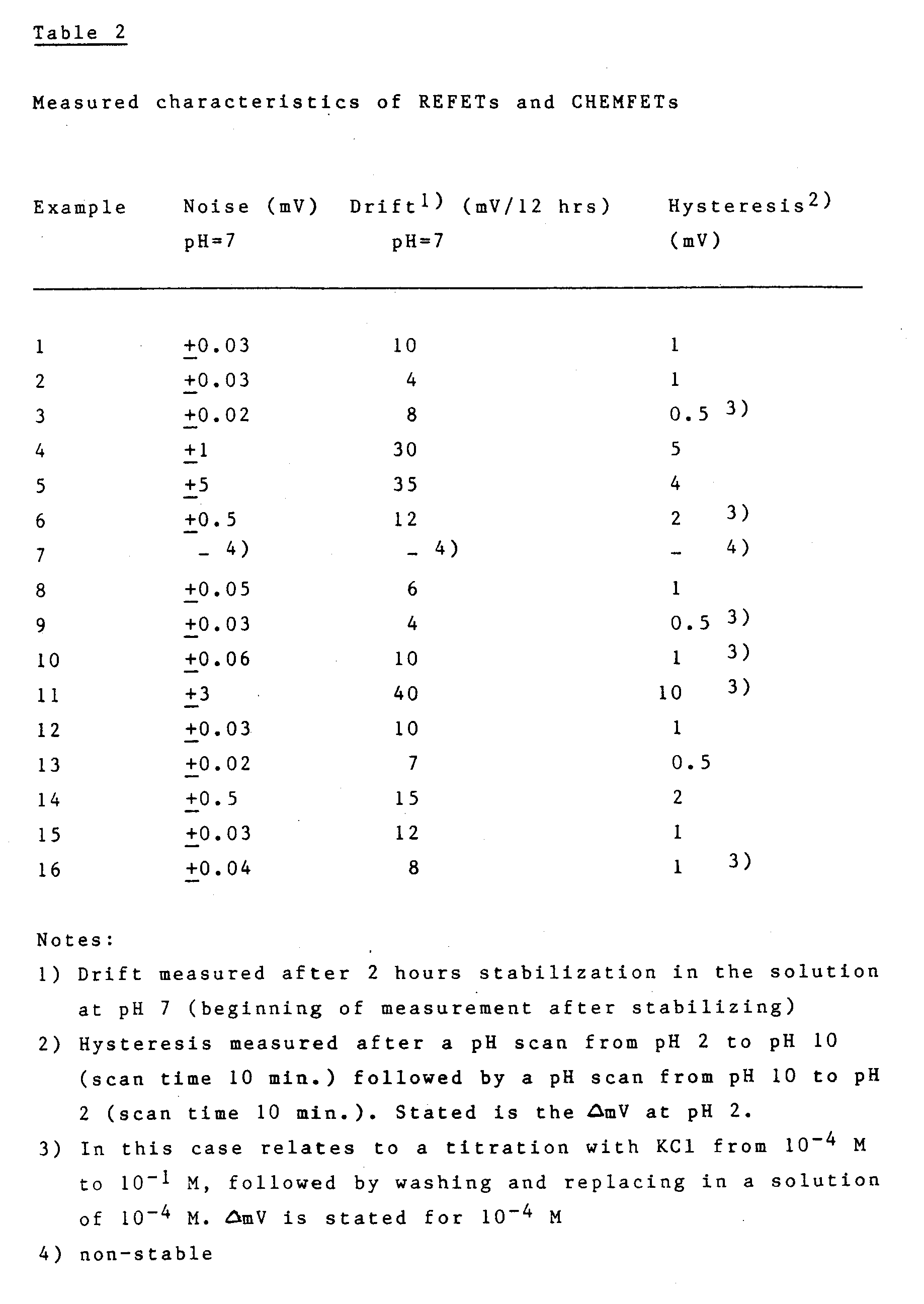
- The modified REFETs and CHEMFETs were measured in accordance with the procedure as described by A.van den Berg, P. Bergveld, D.N. Reinhoudt and E.J.R. Sudhölter, Sensors and Actuators 8 129-148 (1985).
- The results are shown in table 2.
- In addition the reproducibility of the manufactured REFETs and CHEMFETs in mass production is determined and shown in table 3.
- A sensor furnished with a REFET such as that of example 7 gave during measurement at pH 7 a continuous increase in the response. After being exposed to this solution for 5 hours a pH response was observed which corresponded to a non-modified ISFET.
- A sensor containing a REFET as manufactured in example 2 was found after spending a month in a solution at pH 7 to still display the original, even pH response.


Claims (15)
- Process for manufacturing a REFET and/or CHEMFET, comprising:a) covalent bonding of a hydrophilic polymer layer to an isolator layer applied to a semiconductor material;b) the absorption of water or a watery solution into said hydrophilic polymer layer; andc) the binding of a hydrophobic polymer layer to the water holding hydrophilic polymer layer.
- Process as claimed in claim 1, in which the water-holding hydrophilic polymer layer also contains an electrolyte.
- Process as claimed in claim 1 or 2, in which the water-holding hydrophilic polymer layer also contains a buffer.
- Process as claimed in claims 1-3, in which the water holding hydrophilic polymer layer has a thickness of 0.0050-200 µm, and preferably of 0.1-100 µm, and more preferably of 1-50 µm.
- Process as claimed in claims 1-4, in which a receptor for a chemical compound to be measured is incorporated in the hydrophobic polymer layer.
- Process as claimed in claim 5, and at least claim 2, in which an ion to be measured with the CHEMFET also forms part of the electrolyte.
- Process as claimed in claims 1-6, in which the hydrophilic polymer layer is covalently bonded to the isolator layer by a bi-functional organosilicon compound, on the one hand via a group which can be covalently bonded with the isolator layer and on the other via a group which can be covalently bonded to the hydrophilic polymer layer.
- Process as claimed in claim 7, in which the bi-functional organosilicon compound comprises compounds having the structure formulae:
 R, R¹ : alkyl, arylX : halogen, carboxylate, amino, oximY : H, alkyl or aryl


a = 1, 2 or 3 and
p ≧ 2 - Process as claimed in claim 7 or 8, in which the hydrophilic polymer layer is formed by polymerization and comprisesa) monomers with the structure formulae:
 R⁴: -H
-R⁵-OH
R⁵-NH₂
R⁵-SH
R⁵-N(CH₃)₂
R⁵-sugar
R⁵-peptideR⁵: alkyl, arylB : OH, NH₂, b) copolymers with additional monomers having the structure formula III, in which R₄ is now, for example, a C₁-C₃₀ alkyl group,c) mixtures of (co)polymers with a hydrogel, such as gelatin, agar-agar, heparin and polyvinyl pyrrolidone,d) copolymers of the monomers III and IV,e) mixtures of polymers and/or copolymers of the monomers III and IV,f) mixtures of (co)polymers of the monomers III and/or IV with the copolymers as according to point b,g) mixtures of the polymers and/or copolymers named under points a-f.
- Process as claimed in claims 1-9, in which the hydrophobic polymer layer is bonded physically to the hydrophilic, water holding polymer layer.
- Process as claimed in claims 1-9, in which the hydrophobic polymer layer is bonded covalently to the hydrophilic, water-holding polymer layer.
- Process as claimed in claim 11, in which a linking agent is allowed to react with the hydrophilic polymer layer and the hydrophobic polymer is subsequently bonded to said linking agent.
- Process as claimed in claim 12, in which the linking agent has the following structure formula:

Z = halogen, alkoxy, phenoxy or hydroxy,
and the hydrophobic polymer layer is formed by polymerization of monomers containing vinyl groups or by a reaction with "living" polymers. - Process as claimed in claim 6, and if required claims 7-13, in which the receptor is bonded covalently or physically to, or is cross linked to, the hydrophobic polymer layer.
- REFET or CHEMFET manufactured as claimed in any of the claims 1-14.
Priority Applications (1)
| Application Number | Priority Date | Filing Date | Title |
|---|---|---|---|
| AT87201671T ATE98375T1 (en) | 1986-09-05 | 1987-09-03 | PROCESS FOR MAKING A REFET OR A CHEMFET, AND HOW TO MAKE IT. |
Applications Claiming Priority (2)
| Application Number | Priority Date | Filing Date | Title |
|---|---|---|---|
| NL8602242 | 1986-09-05 | ||
| NL8602242A NL8602242A (en) | 1986-09-05 | 1986-09-05 | METHOD FOR MANUFACTURING A REFET OR A CHEMFET, AND THE MANUFACTURED REFET OR CHEMFET |
Publications (3)
| Publication Number | Publication Date |
|---|---|
| EP0258951A2 EP0258951A2 (en) | 1988-03-09 |
| EP0258951A3 EP0258951A3 (en) | 1990-10-10 |
| EP0258951B1 true EP0258951B1 (en) | 1993-12-08 |
Family
ID=19848502
Family Applications (1)
| Application Number | Title | Priority Date | Filing Date |
|---|---|---|---|
| EP87201671A Expired - Lifetime EP0258951B1 (en) | 1986-09-05 | 1987-09-03 | Process for manufacturing a REFET or a CHEMFET, and the manufactured REFET or CHEMFET |
Country Status (6)
| Country | Link |
|---|---|
| US (1) | US4882292A (en) |
| EP (1) | EP0258951B1 (en) |
| JP (1) | JP2564319B2 (en) |
| AT (1) | ATE98375T1 (en) |
| DE (1) | DE3788388T2 (en) |
| NL (1) | NL8602242A (en) |
Cited By (1)
| Publication number | Priority date | Publication date | Assignee | Title |
|---|---|---|---|---|
| DE4202639B4 (en) * | 1991-02-01 | 2004-09-23 | Priva Agro Holding B.V. | Method for producing a membrane for an electrochemical or optical sensor |
Families Citing this family (23)
| Publication number | Priority date | Publication date | Assignee | Title |
|---|---|---|---|---|
| IT1215491B (en) * | 1987-05-15 | 1990-02-14 | Enricerche Spa | BIOSENSOR WITH ENZYMATIC MEMBRANE CHEMICALLY CONNECTED TO A SEMICONDUCTIVE DEVICE. |
| IT1222121B (en) * | 1987-07-24 | 1990-08-31 | Eniricerche Spa | ION SENSOR CONTAINING A SELECTIVE ORGANIC MEMBRANE |
| US5011589A (en) * | 1988-09-30 | 1991-04-30 | Kabushiki Kaisha Toshiba | Solution component sensor device |
| US5102526A (en) * | 1990-05-02 | 1992-04-07 | The University Of Michigan | Solid state ion sensor with silicon membrane |
| JPH05506938A (en) * | 1990-05-02 | 1993-10-07 | ザ ユニヴァーシティ オブ ミシガン | Solid ion sensor with polyurethane membrane |
| DE4017905A1 (en) * | 1990-06-02 | 1991-12-05 | Basf Ag | REFERENCE ELECTRODE FOR CHEMICAL SENSORS |
| NL194838C (en) * | 1991-05-17 | 2003-04-03 | Priva Agro Holding Bv | Metal ion-selective membrane and sensor including this membrane. |
| NL194721C (en) * | 1992-10-15 | 2003-01-07 | Priva Agro Holding Bv | Anion-selective membrane and a sensor provided with it. |
| FR2702566B1 (en) * | 1993-03-08 | 1995-06-09 | Ifremer | INTEGRATED ELECTROCHEMICAL SENSOR FOR PH MEASUREMENT AND ITS MANUFACTURING METHOD. |
| EP0661535A1 (en) * | 1993-12-15 | 1995-07-05 | Hitachi, Ltd. | Ion sensor |
| US6024924A (en) * | 1995-09-29 | 2000-02-15 | Forschungzentrum Julich Gmbh | Biosensor system for detecting organic trace compounds produced by smoldering fires |
| DE19536389C2 (en) * | 1995-09-29 | 2003-06-12 | Forschungszentrum Juelich Gmbh | Biosensor system for measuring one or more, in particular organic, trace components in air caused by plant damage |
| JP2001511245A (en) * | 1996-04-17 | 2001-08-07 | モトローラ・インコーポレイテッド | Apparatus and method for detecting molecules using transistors |
| US5958201A (en) * | 1996-08-26 | 1999-09-28 | Dade Behring Inc. | Sodium ion-selective-electrode membrane having extended uselife |
| EP1085319B1 (en) * | 1999-09-13 | 2005-06-01 | Interuniversitair Micro-Elektronica Centrum Vzw | A device for detecting an analyte in a sample based on organic materials |
| EP1085320A1 (en) | 1999-09-13 | 2001-03-21 | Interuniversitair Micro-Elektronica Centrum Vzw | A device for detecting an analyte in a sample based on organic materials |
| DE10006238A1 (en) * | 2000-02-11 | 2001-08-23 | Siemens Ag | Semiconductor gas sensor with buffer system |
| DE10335163B3 (en) * | 2003-07-30 | 2005-03-03 | Micronas Gmbh | gas sensor |
| JP4557755B2 (en) * | 2004-03-11 | 2010-10-06 | キヤノン株式会社 | Substrate, conductive substrate, and organic field effect transistor manufacturing method |
| US7794584B2 (en) * | 2005-10-12 | 2010-09-14 | The Research Foundation Of State University Of New York | pH-change sensor and method |
| TWI302197B (en) * | 2006-01-04 | 2008-10-21 | Univ Nat Yunlin Sci & Tech | Reference ph sensor, the preparation and application thereof |
| WO2007119690A1 (en) * | 2006-04-12 | 2007-10-25 | Panasonic Corporation | Method of forming organic molecular film structure and organic molecular film structure |
| DE102008041960A1 (en) * | 2008-09-10 | 2010-03-11 | Robert Bosch Gmbh | Measuring sensor, method for analyzing a non-polar liquid, method for producing a measuring sensor |
Family Cites Families (10)
| Publication number | Priority date | Publication date | Assignee | Title |
|---|---|---|---|---|
| JPS5825221B2 (en) * | 1977-12-12 | 1983-05-26 | 株式会社クラレ | FET reference electrode |
| JPS5626250A (en) * | 1979-08-10 | 1981-03-13 | Olympus Optical Co Ltd | Composite chemical sensor |
| DE3020068C2 (en) * | 1979-05-30 | 1983-11-03 | Olympus Optical Co., Ltd., Tokyo | Chemically sensitive measuring cell |
| JPS562546A (en) * | 1979-06-20 | 1981-01-12 | Kuraray Co Ltd | Gas sensor using fet and its manufacture |
| US4490216A (en) * | 1983-02-03 | 1984-12-25 | Molecular Devices Corporation | Lipid membrane electroanalytical elements and method of analysis therewith |
| JPS59182356A (en) * | 1983-04-01 | 1984-10-17 | Hitachi Ltd | Sensitive membrane of anion selective electrode |
| US4650547A (en) * | 1983-05-19 | 1987-03-17 | The Regents Of The University Of California | Method and membrane applicable to implantable sensor |
| NL8400916A (en) * | 1984-03-22 | 1985-10-16 | Stichting Ct Voor Micro Elektr | METHOD FOR MANUFACTURING AN ISFET AND ISFET MADE THEREFORE |
| CA1223039A (en) * | 1984-03-26 | 1987-06-16 | Michael Thompson | Chemical selective sensors utilizing admittance modulated membranes |
| EP0235470B1 (en) * | 1986-01-24 | 1992-11-11 | TERUMO KABUSHIKI KAISHA trading as TERUMO CORPORATION | Ion-sensitive fet sensor |
-
1986
- 1986-09-05 NL NL8602242A patent/NL8602242A/en not_active Application Discontinuation
-
1987
- 1987-09-03 AT AT87201671T patent/ATE98375T1/en not_active IP Right Cessation
- 1987-09-03 DE DE87201671T patent/DE3788388T2/en not_active Expired - Fee Related
- 1987-09-03 EP EP87201671A patent/EP0258951B1/en not_active Expired - Lifetime
- 1987-09-04 US US07/093,014 patent/US4882292A/en not_active Expired - Lifetime
- 1987-09-04 JP JP62222874A patent/JP2564319B2/en not_active Expired - Fee Related
Cited By (1)
| Publication number | Priority date | Publication date | Assignee | Title |
|---|---|---|---|---|
| DE4202639B4 (en) * | 1991-02-01 | 2004-09-23 | Priva Agro Holding B.V. | Method for producing a membrane for an electrochemical or optical sensor |
Also Published As
| Publication number | Publication date |
|---|---|
| EP0258951A2 (en) | 1988-03-09 |
| DE3788388D1 (en) | 1994-01-20 |
| US4882292A (en) | 1989-11-21 |
| EP0258951A3 (en) | 1990-10-10 |
| NL8602242A (en) | 1988-04-05 |
| ATE98375T1 (en) | 1993-12-15 |
| DE3788388T2 (en) | 1994-03-24 |
| JP2564319B2 (en) | 1996-12-18 |
| JPS6388439A (en) | 1988-04-19 |
Similar Documents
| Publication | Publication Date | Title |
|---|---|---|
| US4882292A (en) | Process for manufacturing a REFET or a CHEMFET, and the manufactured REFET or CHEMFET | |
| Sudhölter et al. | Modification of ISFETs by covalent anchoring of poly (hyroxyethyl methacrylate) hydrogel. Introduction of a thermodynamically defined semiconductor-sensing membrane interface | |
| EP0395137B1 (en) | Sensor with antigen chemically bonded to a semiconductor device | |
| Antonisse et al. | Potentiometric anion selective sensors | |
| US5114674A (en) | Added array of molecular chains for interfering with electrical fields | |
| US4562157A (en) | Diagnostic device incorporating a biochemical ligand | |
| US4822681A (en) | Activated polymer solid bodies and processes for the production thereof | |
| Liu et al. | Potentiometric ion-and bioselective electrodes based on asymmetric polyurethane membranes | |
| EP0643299B1 (en) | Ion selective electrodes | |
| KR900702361A (en) | Bio sensor made entirely of micro, its production method and use of copper sensor | |
| Pogorelova et al. | Selective sensing of triazine herbicides in imprinted membranes using ion-sensitive field-effect transistors and microgravimetric quartz crystal microbalance measurements | |
| JPH0567910B2 (en) | ||
| EP0177544B1 (en) | Method of producing an isfet and same isfet | |
| US5035791A (en) | Ion sensor containing a selective organic membrane | |
| Skowronska-Ptasinska et al. | Reference field effect transistors based on chemically modified ISFETs | |
| Wu et al. | Renewable urea sensor based on a self-assembled polyelectrolyte layer | |
| US11261204B2 (en) | Composition for substrate surface modification and method using the same | |
| Clechet et al. | Silica surface sensitization and chemical sensors | |
| EP0270174B1 (en) | Ion-sensitive device | |
| An et al. | Dual‐Amplification of Antigen–Antibody Interactions via Backfilling Gold Nanoparticles on (3‐Mercaptopropyl) Trimethoxysilane Sol‐Gel Functionalized Interface | |
| EP0313161B1 (en) | Sensor with immunochemical membrane chemically bound to a semiconductor device | |
| Bojorge-Ramírez et al. | Amperometric immunosensor for detecting Schistosoma mansoni antibody | |
| Jaffrezic-Renault et al. | Preparation of well-engineered thin molecular layers on semiconductor-based transducers | |
| van der Wal et al. | Covalently bound plasticized PVC membranes for solid state ion-selective devices | |
| EP1413886A1 (en) | Sensor surface |
Legal Events
| Date | Code | Title | Description |
|---|---|---|---|
| PUAI | Public reference made under article 153(3) epc to a published international application that has entered the european phase |
Free format text: ORIGINAL CODE: 0009012 |
|
| AK | Designated contracting states |
Kind code of ref document: A2 Designated state(s): AT BE CH DE FR GB LI LU NL SE |
|
| PUAL | Search report despatched |
Free format text: ORIGINAL CODE: 0009013 |
|
| AK | Designated contracting states |
Kind code of ref document: A3 Designated state(s): AT BE CH DE FR GB LI LU NL SE |
|
| RHK1 | Main classification (correction) |
Ipc: G01N 27/414 |
|
| 17P | Request for examination filed |
Effective date: 19910408 |
|
| RAP1 | Party data changed (applicant data changed or rights of an application transferred) |
Owner name: PRIVA AGRO HOLDING B.V. |
|
| 17Q | First examination report despatched |
Effective date: 19930127 |
|
| GRAA | (expected) grant |
Free format text: ORIGINAL CODE: 0009210 |
|
| AK | Designated contracting states |
Kind code of ref document: B1 Designated state(s): AT BE CH DE FR GB LI LU NL SE |
|
| REF | Corresponds to: |
Ref document number: 98375 Country of ref document: AT Date of ref document: 19931215 Kind code of ref document: T |
|
| REF | Corresponds to: |
Ref document number: 3788388 Country of ref document: DE Date of ref document: 19940120 |
|
| ET | Fr: translation filed | ||
| PLBE | No opposition filed within time limit |
Free format text: ORIGINAL CODE: 0009261 |
|
| STAA | Information on the status of an ep patent application or granted ep patent |
Free format text: STATUS: NO OPPOSITION FILED WITHIN TIME LIMIT |
|
| 26N | No opposition filed | ||
| EAL | Se: european patent in force in sweden |
Ref document number: 87201671.2 |
|
| REG | Reference to a national code |
Ref country code: CH Ref legal event code: NV Representative=s name: OK PAT AG |
|
| REG | Reference to a national code |
Ref country code: GB Ref legal event code: IF02 |
|
| PGFP | Annual fee paid to national office [announced via postgrant information from national office to epo] |
Ref country code: DE Payment date: 20030715 Year of fee payment: 17 Ref country code: BE Payment date: 20030715 Year of fee payment: 17 |
|
| PGFP | Annual fee paid to national office [announced via postgrant information from national office to epo] |
Ref country code: CH Payment date: 20030804 Year of fee payment: 17 |
|
| PGFP | Annual fee paid to national office [announced via postgrant information from national office to epo] |
Ref country code: SE Payment date: 20030808 Year of fee payment: 17 |
|
| PGFP | Annual fee paid to national office [announced via postgrant information from national office to epo] |
Ref country code: LU Payment date: 20030811 Year of fee payment: 17 |
|
| PGFP | Annual fee paid to national office [announced via postgrant information from national office to epo] |
Ref country code: FR Payment date: 20030820 Year of fee payment: 17 |
|
| PGFP | Annual fee paid to national office [announced via postgrant information from national office to epo] |
Ref country code: GB Payment date: 20030903 Year of fee payment: 17 |
|
| PGFP | Annual fee paid to national office [announced via postgrant information from national office to epo] |
Ref country code: AT Payment date: 20030922 Year of fee payment: 17 |
|
| PGFP | Annual fee paid to national office [announced via postgrant information from national office to epo] |
Ref country code: NL Payment date: 20030924 Year of fee payment: 17 |
|
| PG25 | Lapsed in a contracting state [announced via postgrant information from national office to epo] |
Ref country code: LU Free format text: LAPSE BECAUSE OF NON-PAYMENT OF DUE FEES Effective date: 20040903 Ref country code: GB Free format text: LAPSE BECAUSE OF NON-PAYMENT OF DUE FEES Effective date: 20040903 Ref country code: AT Free format text: LAPSE BECAUSE OF NON-PAYMENT OF DUE FEES Effective date: 20040903 |
|
| PG25 | Lapsed in a contracting state [announced via postgrant information from national office to epo] |
Ref country code: SE Free format text: LAPSE BECAUSE OF NON-PAYMENT OF DUE FEES Effective date: 20040904 |
|
| PG25 | Lapsed in a contracting state [announced via postgrant information from national office to epo] |
Ref country code: LI Free format text: LAPSE BECAUSE OF NON-PAYMENT OF DUE FEES Effective date: 20040930 Ref country code: CH Free format text: LAPSE BECAUSE OF NON-PAYMENT OF DUE FEES Effective date: 20040930 Ref country code: BE Free format text: LAPSE BECAUSE OF NON-PAYMENT OF DUE FEES Effective date: 20040930 |
|
| BERE | Be: lapsed |
Owner name: *PRIVA AGRO HOLDING B.V. Effective date: 20040930 |
|
| PG25 | Lapsed in a contracting state [announced via postgrant information from national office to epo] |
Ref country code: NL Free format text: LAPSE BECAUSE OF NON-PAYMENT OF DUE FEES Effective date: 20050401 Ref country code: DE Free format text: LAPSE BECAUSE OF NON-PAYMENT OF DUE FEES Effective date: 20050401 |
|
| GBPC | Gb: european patent ceased through non-payment of renewal fee |
Effective date: 20040903 |
|
| EUG | Se: european patent has lapsed | ||
| REG | Reference to a national code |
Ref country code: CH Ref legal event code: PL |
|
| PG25 | Lapsed in a contracting state [announced via postgrant information from national office to epo] |
Ref country code: FR Free format text: LAPSE BECAUSE OF NON-PAYMENT OF DUE FEES Effective date: 20050531 |
|
| NLV4 | Nl: lapsed or anulled due to non-payment of the annual fee |
Effective date: 20050401 |
|
| REG | Reference to a national code |
Ref country code: FR Ref legal event code: ST |
|
| BERE | Be: lapsed |
Owner name: *PRIVA AGRO HOLDING B.V. Effective date: 20040930 |