EP0254886B1 - Serially-accessed type memory device - Google Patents
Serially-accessed type memory device Download PDFInfo
- Publication number
- EP0254886B1 EP0254886B1 EP87109345A EP87109345A EP0254886B1 EP 0254886 B1 EP0254886 B1 EP 0254886B1 EP 87109345 A EP87109345 A EP 87109345A EP 87109345 A EP87109345 A EP 87109345A EP 0254886 B1 EP0254886 B1 EP 0254886B1
- Authority
- EP
- European Patent Office
- Prior art keywords
- data
- dba
- dbb
- output
- switching
- Prior art date
- Legal status (The legal status is an assumption and is not a legal conclusion. Google has not performed a legal analysis and makes no representation as to the accuracy of the status listed.)
- Expired - Lifetime
Links
Images


Classifications
-
- G—PHYSICS
- G11—INFORMATION STORAGE
- G11C—STATIC STORES
- G11C11/00—Digital stores characterised by the use of particular electric or magnetic storage elements; Storage elements therefor
-
- G—PHYSICS
- G11—INFORMATION STORAGE
- G11C—STATIC STORES
- G11C7/00—Arrangements for writing information into, or reading information out from, a digital store
- G11C7/10—Input/output [I/O] data interface arrangements, e.g. I/O data control circuits, I/O data buffers
- G11C7/1015—Read-write modes for single port memories, i.e. having either a random port or a serial port
- G11C7/103—Read-write modes for single port memories, i.e. having either a random port or a serial port using serially addressed read-write data registers
Definitions
- the present invention relates to a serially-accessed type memory device.
- a series of operations are performed in one cycle which is determined in accordance with control signals or address signals of an external input. These operations include accepting and decoding an externally input address in a column direction, activation of a column selection line to transfer data to a data bus line, and activation of an output driver to output the data.
- a serially-accessed type memory device which comprises first and second data sources selectively connected to corresponding first and second data lines.
- a multiplexer selectively connects either of the first and second data lines to an output means.
- EP-A-0 152 954 a semiconductor memory device is known having first and second data sources, first and second data lines, first and second connecting means, output means and switching means.
- US-4 344 156 discloses a memory system for rapidly transferring data between a plurality of successive memory locations and a data output bus.
- rapid writing of data into the memory is effected by imcluding a number of data buffers which receive income data and are adapted to output that data to a number of successive memory locations.
- Each buffer is controlled by a sequentially enabled decoder.
- EP-A-0 211 565 falling under Article 54(3) EPC describes a random access memory addressed in a sequential mode. In this mode, alternate cells from each of two sets of cells are addressed in such a manner that present data are placed on one data line while preceeding data are read from the other data line.
- the present invention has been made in consideration of the above situation, and has as its object to provide a memory device having a column-direction serial access function, which is capable of reducing a cycle time.
- the serially-accessed type memory device comprises a first data source and a second data source; a first data line and a second data line; first and second connecting means for selectively connecting said first data source to said first data line and said second data source to said second data line, respectively; output means for outputting data supplied from either of said first and second data sources through a corresponding one of said first and second data lines; and first switching means for selectively connecting either of said first and second data lines to said output means;
- said first connecting means include a first serial address generator for generating first serial address data updated in synchronism with a switching operation of said switching means; a first decoding means for decoding outputs from said first serial address generator; and first gating means for connecting said first data source to said first data line in accordance with the output of the first decoding means;
- said second connecting means include a second serial address generator for generating second address data updated in synchronism with a switching operation of said switching means; a second decoding means for decoding outputs from
- the serially-accessed type memory device comprises a first data source and a second data source; a first data line and a second data line; first and second connecting means for selectively connecting said first data source to said first data line and said second data source to said second data line, respectively; input means for supplying write data to either of said first and second data sources through a corresponding one of said first and second data lines; and first switching means for selectively supplying the write data from said input means to either of said first and second data lines; wherein said first connecting means include a first address generator for generating first address data updated in synchronism with a switching operation of said switching means; first gating means for connecting said first data source to said first data line in accordance with a content of the first address data; said second connecting means include a second address generator for generating second address data updated in synchronism with a switching operation of said switching means; second gating means for connecting said second data source to said second data line in accordance with a content of the second
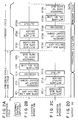
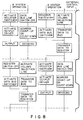
- Fig. 1 is a block diagram of an internal circuit arrangement of a column-direction serially-accessed memory according to the embodiment of the present invention
- Figs. 2A to 2D are flow charts for explaining an operation thereof.
- two systems A and B for selecting/fetching data are provided in a single chip.
- Reference numerals 20 and 22 denote A data registers (or A bit lines); 21 and 23, B data registers (or B bit lines); 24 and 26, A column selecting gates; 25 and 27, B column selecting gates; 28 and 30, A column selecting line drivers; 29 and 31, B column selecting line drivers; 32 and 34, A decoders; 33 and 35, B decoders; 36, an A serial address generator; 37, a B serial address generator; 38, an A data bus switcher; 39, a B data bus switcher; 40, an output driver; CA0 and CA1, A column selecting lines; CB0 and CB1, B column selecting lines; DBA and DBA , A data bus lines; DBB and DBB , B data bus lines; AA, an A address bus line; AB, a B address bus line; and SO, a data output. All of these circuit elements can be formed in a one-chip IC pellet.
- FIG. 1 A data read operation of the memory shown in Fig. 1 will be described. Assume that registers (or bit lines) 20, 21, 22, and 23 are accessed in this order. Note that a description will be made with reference to a case wherein the present cycle is a cycle for accessing data of register 22 which belongs to system A.
- switcher 38 is turned off, as shown in step ST1 of Fig. 2B, and switcher 39 is activated and hence is in an ON state, as shown in step ST11 of Fig. 2C.
- steps ST12 and ST13 data of register 21 are transferred to driver 40 through bus lines DBB and DBB .
- step ST2 when system A is disconnected from driver 40 by OFF switcher 38, an address of the present cycle is set in generator 36 (step ST2), and decoder 34 corresponding to the set address is selected (step ST3). Then, selecting line CA1 is activated (step ST4), and data of register 22 are transferred to bus lines DBA and DBA , as shown in step ST5.
- switcher 39 is turned off as shown in step ST31 of Fig. 2C, and switcher 38 is activated and hence is in an ON state as shown in step ST21 of Fig. 2B.
- bus lines DBA and DBA are connected to driver 40 through ON switcher 38 (step ST22).
- the data of register 22 is transferred to driver 40 as shown in step ST23, and data SO transferred from driver 40 is output.
- step ST32 When system B is disconnected from driver 40, generator 37 is activated, and the address is counted up (or down) as shown in step ST32. Decoder 35 is selected in correspondence to the counted-up (or -down) address (step ST33), and selecting line CB1 is activated (step ST34). Then, the data of register 23 are transferred to bus lines DBB and DBB as shown in step ST35, thereby completing set-up for access in the next cycle.
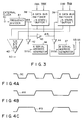
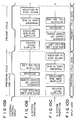
- Fig. 3 shows hardware for alternately operating systems A and B in the arrangement shown in Fig. 1.
- Figs. 4A to 4C shown waveforms for explaining an operation of the hardware shown in Fig. 3.
- External clock SC (Fig. 4A) having a period of one cycle shown in Fig. 2A is converted through 1/2 frequency divider 41 into pulse ⁇ A (Fig. 4B) for selecting system A.
- Pulse ⁇ A is supplied to a 3-state buffer which constitutes switcher 38.
- buffer 38 connects bus lines DBA and DBA to driver 40.
- pulse ⁇ A is logic "0"
- buffer 38 is opened, and bus lines DBA and DBA are disconnected from driver 40.
- Pulse ⁇ A is phase-inverted, via inverter 42, to be a synchronous signal having the same waveform as that of pulse ⁇ B of Fig. 4C, and is supplied to a clock input terminal of an address counter in generator 36.
- a content (address data) of output AA of generator 36 is updated (counted up or down) by 1 at the fall timing of pulse ⁇ A.
- pulse ⁇ A is phase-inverted, by inverter 43, to be pulse ⁇ B of Fig. 4C.
- Pulse ⁇ B is further phase-inverted, by inverter 44, to be a synchronous signal having the same waveform as that of pulse ⁇ A of Fig. 4B, and is supplied to a clock input terminal of an address counter in generator 37.
- a content (address data) of output AB of generator 37 is updated (counted up or down) by 1 at the fall timing of pulse ⁇ B.
- pulse ⁇ B is supplied to a 3-state buffer which constitutes switcher 39.
- buffer 39 connects bus lines DBB and DBB to driver 40. (At this time, since pulse ⁇ A is logic "0", driver 40 is disconnected from bus lines DBA and DBA ).
- switchers 38 and 39 are alternately opened/closed every one period (one cycle of Fig. 2A) of clock SC so as to alternately select systems A and B. Then, in synchronism with each alternate selection, the contents of data AA and AB are updated by 1 for every two periods (two cycle of Fig. 2A) of clock SC.
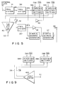
- Fig. 5 shows hardware wherein switchers 38 and 39 shown in Fig. 3 are replaced with registers/switchers 380 and 390, respectively.
- systems A and B are alternately switched in the order of A ⁇ B ⁇ A ⁇ B ⁇ ....
- the same data an be alternately switched twice as in the order of A ⁇ A ⁇ B ⁇ B ⁇ A ⁇ A ⁇ B ⁇ B ⁇ ....
- This two-time alternate switching operation is exemplified in Figs. 6A and 6B.
- 1/2 frequency divider 381 is inserted between frequency divider 41 and each of registers/switchers 380 and 390, in order that the connections for registers/switchers 380 and 390 are alternatively switched for each two cycles. More specifically, frequency-divided output ⁇ N from divider 381 is applied to register/switcher 380, and the phase-inverted signal of output ⁇ N, obtained via inverter 43, is applied to register/switcher 390. In this circuit configuration, output signal ⁇ N from divider 381 has a period two times longer than the period of clock ⁇ A.
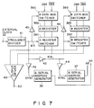
- Fig. 7 shows a modification of switchers 38 and 39 shown in Fig. 3.
- switcher 38a (3-state buffer) is conducted by an output of logic "1" from inverter 45 while switcher 38c (3-state buffer) is opened by logic "0" of pulse ⁇ A, thereby storing the data of bus lines DBA and DBA in register 38b.
- switcher 39c While the data of system A is stored, switcher 39c is conducted by logic "1" of pulse ⁇ B, and a content of register 39b is supplied to buffer 40. At this time, since an output from inverter 46 is logic "0", switcher 39a is opened.
- Fig. 8 shows an operation of the modification shown in Fig. 7.
- a time required for one cycle is reduced by the arrangement shown in Fig. 7. That is, five steps ST1 to ST5 in one cycle of Fig. 2B are reduced to three serial steps in Fig. 8 when viewed along the serial flow of time. Similarly, five serial steps ST31 to ST35 in Fig. 2C are reduced to three serial steps in Fig. 8.
- the number of processing steps, including time-serially in one cycle is reduced, so that a cycle time can be reduced more effectively.
- Fig. 9 shows a modified portion when the arrangement (for reading out data) shown in Fig. 1 is modified to that for writing data.
- Writing input data SI is converted into data DB in phase with data SI and data DB opposite phase to data SI through input buffer 400.
- Data DB and DB are supplied to bus lines DBA and DBA through data bus switcher 386, and are supplied to bus lines DBB and DBB through switcher 396.
- the other portions of the arrangement of Fig. 9 can be the same as those of the arrangement shown in Fig. 1.
- Figs. 10A and 10B show a data write operation of the arrangement, obtained by applying the modified portion shown in Fig. 9 to the arrangement shown in Fig. 1.
- systems A and B are operated with a time shift of about 1/2 cycle. For this reason, one cycle time of these embodiments only requires a time substantially half that of a conventional one cycle including steps ST1 to ST5 and ST21 to ST23. Therefore, a cycle time can be reduced. That is, according to the present invention, both the systems (A, B) are alternately operated so that data is set up in one system (e.g., A) while data is output in the other (e.g., B), thereby reducing the cycle time.
- the present invention is applied in a single semiconductor memory chip and two systems (A and B) of data selecting/fetching circuits are provided therein, a high speed memory operation can be achieved by the single chip.
- the present invention can be applied to all the memories except a random access type (i.e., wherein an address to be accessed next to the present address is determined). Therefore, the present invention can also be applied to reduction in a read cycle time of a serially-accessed type semiconductor ROM or of a CDROM having two-channel optical pickup systems, etc.
Description
- The present invention relates to a serially-accessed type memory device.
- In a conventional random access memory, a series of operations are performed in one cycle which is determined in accordance with control signals or address signals of an external input. These operations include accepting and decoding an externally input address in a column direction, activation of a column selection line to transfer data to a data bus line, and activation of an output driver to output the data.
- On the other hand, in a memory having a serial access function, an address to be accessed next is determined, unlike in the random access memory. For this reason, the above series of operations need not be performed in one cycle determined by the externally input signals, but can be set up (prepared) beforehand.
- However, in the arrangement where only one data transmission system is provided, the above series of operations must be performed by a single data transfer system regardless of an operation state from which an access in a present cycle is started. For this reason, although an access itself can be performed at a high speed, it is difficult to reduce a cycle time.
- From "Elektronik", Vol. 31, No. 15, July 1982, pages 27 - 30, Munich, DE; P. Mattos et al.: "Nibble-Mode beschleunigt Speicherzugriff" a serially-accessed type memory device is known which comprises first and second data sources selectively connected to corresponding first and second data lines. A multiplexer selectively connects either of the first and second data lines to an output means.
- From EP-A-0 152 954 a semiconductor memory device is known having first and second data sources, first and second data lines, first and second connecting means, output means and switching means.
- US-4 344 156 discloses a memory system for rapidly transferring data between a plurality of successive memory locations and a data output bus. In this system, rapid writing of data into the memory is effected by imcluding a number of data buffers which receive income data and are adapted to output that data to a number of successive memory locations. Each buffer is controlled by a sequentially enabled decoder.
- EP-A-0 211 565 falling under Article 54(3) EPC describes a random access memory addressed in a sequential mode. In this mode, alternate cells from each of two sets of cells are addressed in such a manner that present data are placed on one data line while preceeding data are read from the other data line.
- The present invention has been made in consideration of the above situation, and has as its object to provide a memory device having a column-direction serial access function, which is capable of reducing a cycle time.
- In order to solve the object of the present invention, the serially-accessed type memory device comprises a first data source and a second data source;
a first data line and a second data line;
first and second connecting means for selectively connecting said first data source to said first data line and said second data source to said second data line, respectively;
output means for outputting data supplied from either of said first and second data sources through a corresponding one of said first and second data lines; and
first switching means for selectively connecting either of said first and second data lines to said output means;
wherein
said first connecting means include
a first serial address generator for generating first serial address data updated in synchronism with a switching operation of said switching means;
a first decoding means for decoding outputs from said first serial address generator; and
first gating means for connecting said first data source to said first data line in accordance with the output of the first decoding means;
said second connecting means include
a second serial address generator for generating second address data updated in synchronism with a switching operation of said switching means;
a second decoding means for decoding outputs from said second serial address generator; and
second gating means for connecting said second data source to said second data line in accordance with the output of the second decoding means; and
an updating timing of the first address data is offset from an updating timing of the second address data, whereby present data are placed on the first or second data line while preceding data are read from the second or first data line, respectively through the switching means and the output means. - Furthermore, in order to solve the above object of the present invention, the serially-accessed type memory device comprises a first data source and a second data source;
a first data line and a second data line;
first and second connecting means for selectively connecting said first data source to said first data line and said second data source to said second data line, respectively;
input means for supplying write data to either of said first and second data sources through a corresponding one of said first and second data lines; and
first switching means for selectively supplying the write data from said input means to either of said first and second data lines;
wherein
said first connecting means include
a first address generator for generating first address data updated in synchronism with a switching operation of said switching means;
first gating means for connecting said first data source to said first data line in accordance with a content of the first address data;
said second connecting means include
a second address generator for generating second address data updated in synchronism with a switching operation of said switching means;
second gating means for connecting said second data source to said second data line in accordance with a content of the second address data; and
an updating timing of the first address data is offset from an updating timing of the second address data, whereby present data are placed on the first or second data line while preceding data are input through the second or first data line, respectively through the second switching means and the input means. - Advantageous embodiments are given in the dependent claims.
- This invention can be more fully understood from the following detailed description when taken in conjunction with the accompanying drawings, in which:
- Fig. 1
- is a block diagram of an essential part of a read section used when the present invention is applied to a serially-accessed type semiconductor memory,
- Figs. 2A to 2D
- are flow charts for explaining a data read operation of the meoroy shown in Fig. 1;
- Fig. 3
- is a block diagram of hardware for alternately operating two data transfer systems (A and B) in the arrangement shown in Fig. 1;
- Figs. 4a to 4C
- are views of waveforms for explaining an operation of the hardware shown in Fig. 3;
- Fig. 5
- is a block diagram of a modification of the hardware shown in Fig. 3; in which data bus switchers (38 and 39) are replaced with registers (380 and 390);
- Fig.s 6A and 6B
- are flow charts for explaining an operation of the memory shown in Fig. 1 using the hardware shown in Fig. 5;
- Fig. 7
- is a block diagram of a modification of the hardware shown in Fig. 3; showing hardware capable of reducing a cycle time of the memory shown in Fig. 1 shorter than that obtained by the hardware shown in Fig. 3;
- Fig. 8
- is a flow chart for explaining an operation of the memory shown in Fig. 1 using the hardware shown in Fig. 7;
- Fig. 9
- is a block diagram partially showing a changed portion used when the arrangement shown in Fig. 1 is applied for data writing; and
- Figs. 10A to 10D
- are flow charts for explaining a data write operation used when the arrangement shown in Fig. 9 is applied to the memory shown in Fig. 1.
- An embodiment of the present invention will now be described with reference to the accompanying drawings. Fig. 1 is a block diagram of an internal circuit arrangement of a column-direction serially-accessed memory according to the embodiment of the present invention, and Figs. 2A to 2D are flow charts for explaining an operation thereof. According to this embodiment, in a semiconductor memory having a column-direction serial access function, two systems A and B for selecting/fetching data are provided in a single chip.
Reference numerals 20 and 22 denote A data registers (or A bit lines); 21 and 23, B data registers (or B bit lines); 24 and 26, A column selecting gates; 25 and 27, B column selecting gates; 28 and 30, A column selecting line drivers; 29 and 31, B column selecting line drivers; 32 and 34, A decoders; 33 and 35, B decoders; 36, an A serial address generator; 37, a B serial address generator; 38, an A data bus switcher; 39, a B data bus switcher; 40, an output driver; CA0 and CA1, A column selecting lines; CB0 and CB1, B column selecting lines; DBA andDBA , A data bus lines; DBB andDBB , B data bus lines; AA, an A address bus line; AB, a B address bus line; and SO, a data output. All of these circuit elements can be formed in a one-chip IC pellet. - A data read operation of the memory shown in Fig. 1 will be described. Assume that registers (or bit lines) 20, 21, 22, and 23 are accessed in this order. Note that a description will be made with reference to a case wherein the present cycle is a cycle for accessing data of register 22 which belongs to system A.
- In this case, since the preceding cycle is a cycle for accessing from system B,
switcher 38 is turned off, as shown in step ST1 of Fig. 2B, andswitcher 39 is activated and hence is in an ON state, as shown in step ST11 of Fig. 2C. As shown in steps ST12 and ST13, data of register 21 are transferred todriver 40 through bus lines DBB andDBB . - On the other hand, when system A is disconnected from
driver 40 byOFF switcher 38, an address of the present cycle is set in generator 36 (step ST2), anddecoder 34 corresponding to the set address is selected (step ST3). Then, selecting line CA1 is activated (step ST4), and data of register 22 are transferred to bus lines DBA andDBA , as shown in step ST5. - When a present cycle, subsequent to the above cycle, begins (Fig. 2A),
switcher 39 is turned off as shown in step ST31 of Fig. 2C, andswitcher 38 is activated and hence is in an ON state as shown in step ST21 of Fig. 2B. Then, bus lines DBA andDBA are connected todriver 40 through ON switcher 38 (step ST22). The data of register 22 is transferred todriver 40 as shown in step ST23, and data SO transferred fromdriver 40 is output. - When system B is disconnected from
driver 40,generator 37 is activated, and the address is counted up (or down) as shown in step ST32. Decoder 35 is selected in correspondence to the counted-up (or -down) address (step ST33), and selecting line CB1 is activated (step ST34). Then, the data of register 23 are transferred to bus lines DBB andDBB as shown in step ST35, thereby completing set-up for access in the next cycle. - Fig. 3 shows hardware for alternately operating systems A and B in the arrangement shown in Fig. 1. Figs. 4A to 4C shown waveforms for explaining an operation of the hardware shown in Fig. 3.
- External clock SC (Fig. 4A) having a period of one cycle shown in Fig. 2A is converted through 1/2
frequency divider 41 into pulse φA (Fig. 4B) for selecting system A. Pulse φA is supplied to a 3-state buffer which constitutesswitcher 38. When pulse φA is logic "1",buffer 38 connects bus lines DBA andDBA todriver 40. When pulse φA is logic "0",buffer 38 is opened, and bus lines DBA andDBA are disconnected fromdriver 40. - Pulse φA is phase-inverted, via
inverter 42, to be a synchronous signal having the same waveform as that of pulse φB of Fig. 4C, and is supplied to a clock input terminal of an address counter ingenerator 36. A content (address data) of output AA ofgenerator 36 is updated (counted up or down) by 1 at the fall timing of pulse φA. - In addition, pulse φA is phase-inverted, by
inverter 43, to be pulse φB of Fig. 4C. Pulse φB is further phase-inverted, byinverter 44, to be a synchronous signal having the same waveform as that of pulse φA of Fig. 4B, and is supplied to a clock input terminal of an address counter ingenerator 37. A content (address data) of output AB ofgenerator 37 is updated (counted up or down) by 1 at the fall timing of pulse φB. - On the other hand, In order to select system B, pulse φB is supplied to a 3-state buffer which constitutes
switcher 39. When pulse φB is logic "1",buffer 39 connects bus lines DBB andDBB todriver 40. (At this time, since pulse φA is logic "0",driver 40 is disconnected from bus lines DBA andDBA ). - As described above,
switchers - Fig. 5 shows hardware wherein
switchers switchers - When the above two-time alternate switching operation is to be performed, 1/2
frequency divider 381 is inserted betweenfrequency divider 41 and each of registers/switchers switchers divider 381 is applied to register/switcher 380, and the phase-inverted signal of output φN, obtained viainverter 43, is applied to register/switcher 390. In this circuit configuration, output signal φN fromdivider 381 has a period two times longer than the period of clock φA. - In the A system, the data transmission from bus lines DBA,
DBA to register 380 is carried out at the timing of the falling edge of external control clock input SC, provided φN = logic "1". After completion of the data transmission, register 380 is disconnected from bus lines DBA,DBA . Meanwhile, during the period of φN = logic "1", register 380 is connected tooutput driver 40. - In the B system, the data transmission from bus lines DBB,
DBB to register 390 is carried out at the timing of the falling edge of external control clock input SC, provided φN = logic "0". After completion of the data transmission, register 390 is disconnected from bus lines DBB,DBB . Meanwhile, during the period of φN = logic "0", register 390 is connected tooutput driver 40. - In the embodiment of Fig. 5, the contents of address AA (or AB) are required to be fixed during the two-time transmission of the same data DBA (or DBB). To satisfy this requirement, 1/2
frequency divider 361 is inserted betweenfrequency divider 41 and each ofaddress generators divider 41 is applied tofrequency divider 361 viainverter 42. Frequency-divided output φN' fromdivider 361 is applied to addressgenerator 36, and is applied, viainverter 44, to addressgenerator 37. Note here that output φN' fromdivider 361 is to be activated one cycle in advance of the activation of output φN fromdivider 381. - According to the embodiment of Fig. 5, when 1/N (N is a natural number) frequency dividers are used both for
dividers - When the same data is transferred a plurality of times as shown in Fig. 5, reliability of a content of the transferred data can be improved. However, since an operation speed of the memory is reduced, the hardware shown in Fig. 5 may be adopted as necessary.
- Fig. 7 shows a modification of
switchers inverter 45 while switcher 38c (3-state buffer) is opened by logic "0" of pulse φA, thereby storing the data of bus lines DBA andDBA inregister 38b. - While the data of system A is stored, switcher 39c is conducted by logic "1" of pulse φB, and a content of
register 39b is supplied to buffer 40. At this time, since an output frominverter 46 is logic "0", switcher 39a is opened. - When φA = logic "1" and φB = logic "0" in the next cycle, a content of
register 38b is supplied todriver 40, and at the same time, the data of bus lines DBB andDBB are stored inregister 39b. - Fig. 8 shows an operation of the modification shown in Fig. 7. As will be seen from a comparison of the flow chart shown in Fig. 8 with those shown in Figs. 2B and 2C, a time required for one cycle is reduced by the arrangement shown in Fig. 7. That is, five steps ST1 to ST5 in one cycle of Fig. 2B are reduced to three serial steps in Fig. 8 when viewed along the serial flow of time. Similarly, five serial steps ST31 to ST35 in Fig. 2C are reduced to three serial steps in Fig. 8. Thus, the number of processing steps, including time-serially in one cycle, is reduced, so that a cycle time can be reduced more effectively.
- Fig. 9 shows a modified portion when the arrangement (for reading out data) shown in Fig. 1 is modified to that for writing data. Writing input data SI is converted into data DB in phase with data SI and data
DB opposite phase to data SI throughinput buffer 400. Data DB andDB are supplied to bus lines DBA andDBA through data bus switcher 386, and are supplied to bus lines DBB andDBB through switcher 396. The other portions of the arrangement of Fig. 9 can be the same as those of the arrangement shown in Fig. 1. Figs. 10A and 10B show a data write operation of the arrangement, obtained by applying the modified portion shown in Fig. 9 to the arrangement shown in Fig. 1. - According to the embodiments as shown in Fig. 1 etc., systems A and B are operated with a time shift of about 1/2 cycle. For this reason, one cycle time of these embodiments only requires a time substantially half that of a conventional one cycle including steps ST1 to ST5 and ST21 to ST23. Therefore, a cycle time can be reduced. That is, according to the present invention, both the systems (A, B) are alternately operated so that data is set up in one system (e.g., A) while data is output in the other (e.g., B), thereby reducing the cycle time. In addition, when the present invention is applied in a single semiconductor memory chip and two systems (A and B) of data selecting/fetching circuits are provided therein, a high speed memory operation can be achieved by the single chip.
- Note that the present invention can be applied to all the memories except a random access type (i.e., wherein an address to be accessed next to the present address is determined). Therefore, the present invention can also be applied to reduction in a read cycle time of a serially-accessed type semiconductor ROM or of a CDROM having two-channel optical pickup systems, etc.
Claims (8)
- A serially-accessed type memory device comprising:- a first data source (20, 22) and a second data source (21, 23);- a first data line (DBA) and a second data line (DBB);- first and second connecting means (24, 26, 28, 30, 32, 34, 36 and 25, 27, 29, 31, 33, 35, 37) for selectively connecting said first data source (20, 22) to said first data line (DBA) and said second data source (21, 23) to said second data line (DBB), respectively;- output means (40) for outputting data (SO) supplied from either of said first and second data sources (20 to 23) through a corresponding one of said first and second data lines (DBA, DBB); and- first switching means (38, 39) for selectively connecting either of said first and second data lines (DBA, DBB) to said output means (40);wherein :- said first connecting means (24, 26, 28, 30, 32, 34 and 36) include-- a first serial address generator (36) for generating first serial address data (AA) updated in synchronism with a switching operation of said switching means (38, 39);-- a first decoding means (32, 34) for decoding outputs from said first serial address generator (36); and-- first gating means (24, 26, 28, 30, 32, 34) for connecting said first data source (20, 22) to said first data line (DBA) in accordance with the output of the first decoding means (32, 34);- said second connecting means (25, 27, 29, 31, 33, 35, 37) include-- a second serial address generator (37) for generating second address data (AB) updated in synchronism with a switching operation of said switching means (38, 39);-- a second decoding means (33, 35) for decoding outputs from said second serial address generator (37); and-- second gating means (25, 27, 29, 31, 33, 35) for connecting said second data source (21, 23) to said second data line (DBB) in accordance with the output of the second decoding means (33, 35); and- an updating timing of the first address data (AA) is offset from an updating timing of the second address data (AB), whereby present data are placed on the first or second data line while preceding data are read from the second or first data line, respectively, through the switching means and the output means.
- A memory device according to claim 1, characterized in that:
a switching operation of said switching means (38, 39) is performed such that a first interval (ST1 - ST5, ST21 - ST23), from the timing at which one of said first data sources (20, 22) is accessed by said first connecting means (24, 26, 28, 30, 32, 34, 36) to the timing at which data (DBA = SO) of one of said first data sources (20, 22) is output from said output means (40); partially overlaps a second interval (ST31 - ST35, ST11 - ST13), from the timing at which one of said second data sources (21, 23) is accessed by said second connecting means (25, 27, 29, 31, 33, 35, 37) to the timing at which data (DBB = SO) of one of said second data sources (21, 23) is output from said output means (40). - A memory device according to claim 2, characterized in that:
the switching operation of said switching means is performed every N operation cycles of said memory device, wherein N is an integer of 1 or more, and one bit of data is read out during one operation cycle. - A memory device according to claim 3, characterized in that:
said switching means (38, 39) includes first buffer means (38) for selectively connecting said first data line (DBA) to said output means (40), and second buffer means (39) for selectively connecting said second data line (DBB) to said output means (40), and said first and second buffer means (38, 39) are alternately opened/closed every N operation cycles to perform the switching operation. - A memory device according to any one of claims 1 to 3, characterized in that:
said switching means (38, 39) includes first register means (3809, 38a - 38c) for temporarily storing data from either of said first data sources (20, 22) and selectively supplying the stored data to said output means (40), and second register means (390, 39a - 39c) for temporarily storing data from either of said second data sources (21, 23) and selectively supplying the stored data to said output means (40), and that said first and second register means (380, 390, 38a - 38c, 39a - 39c) are alternately operated to perform a selective supply operation. - A memory device according to claim 5, further comprising:
control means (41 - 46) for controlling the switching operation of said first and second register means (380, 390, 38a - 38c, 39a - 39c), such that data from either of said second data sources (21, 23) is temporarily stored in said second register means (390, 39a - 39c) during an interval wherein the data temporarily stored in said first register means (380, 39a - 38c) is supplied to said output means (40), and such that data from either of said first data sources (20, 22) is temporarily stored in said first register means (380, 38a - 38c) during an interval wherein the data temporarily stored in said second register means (390, 39a - 39c) is supplied to said output means (40). - A serially-accessed type memory device comprising:- a first data source (20, 22) and a second data source (21, 23);- a first data line (DBA) and a second data line (DBB);- first and second connecting means (24, 26, 28, 30, 32, 34, 36 and 25, 27, 29, 31, 33, 35, 37) for selectively connecting said first data source (20, 22) to said first data line (DBA) and said second data source (21, 23) to said second data line (DBB), respectively;- input means (400) for supplying write data (S1) to either of said first and second data sources (20 to 23) through a corresponding one of said first and second data lines (DBA, DBB); and- first switching means (386, 396) for selectively supplying the write data (S1) from said input means (400) to either of said first and second data lines (DBA, DBB);wherein :- said first connecting means (24, 26, 28, 30, 32, 34 and 36) include-- a first address generator (36) for generating first address data (AA) updated in synchronism with a switching operation of said switching means (38, 39);-- first gating means (24, 26, 28, 30, 32, 34) for connecting said first data source (20, 22) to said first data line (DBA) in accordance with a content of the first address data (AA);- said second connecting means (25, 27, 29, 31, 33, 35, 37) include-- a second address generator (37) for generating second address data (AB) updated in synchronism with a switching operation of said switching means (38, 39);-- second gating means (25, 27, 29, 31, 33, 35) for connecting said second data source (21, 23) to said second data line (DBB) in accordance with a content of the second address data (AB); and- an updating timing of the first address data (AA) is offset from an updating timing of the second address data (AB), whereby present data are placed on the first or second data line while preceding data are input through the second or first data line, respectively through the second switching means and the input means.
- A memory device according to claim 8, further comprising:
output means (40) for outputting read data (SO) output from either of said first and second data sources (20 - 23) through a corresponding one of said first and second data lines (DBA, DBB); and
read switching means (38, 39) for selectively connecting either of said first and second data lines (DBA, DBB) to said output means (40).
Applications Claiming Priority (2)
| Application Number | Priority Date | Filing Date | Title |
|---|---|---|---|
| JP61151582A JPS639096A (en) | 1986-06-30 | 1986-06-30 | Semiconductor memory |
| JP151582/86 | 1986-06-30 |
Publications (3)
| Publication Number | Publication Date |
|---|---|
| EP0254886A2 EP0254886A2 (en) | 1988-02-03 |
| EP0254886A3 EP0254886A3 (en) | 1990-02-14 |
| EP0254886B1 true EP0254886B1 (en) | 1993-06-16 |
Family
ID=15521664
Family Applications (1)
| Application Number | Title | Priority Date | Filing Date |
|---|---|---|---|
| EP87109345A Expired - Lifetime EP0254886B1 (en) | 1986-06-30 | 1987-06-29 | Serially-accessed type memory device |
Country Status (4)
| Country | Link |
|---|---|
| EP (1) | EP0254886B1 (en) |
| JP (1) | JPS639096A (en) |
| KR (1) | KR960001781B1 (en) |
| DE (1) | DE3786204T2 (en) |
Families Citing this family (1)
| Publication number | Priority date | Publication date | Assignee | Title |
|---|---|---|---|---|
| JPH0283891A (en) * | 1988-09-20 | 1990-03-23 | Fujitsu Ltd | Semiconductor memory |
Citations (1)
| Publication number | Priority date | Publication date | Assignee | Title |
|---|---|---|---|---|
| EP0211565A2 (en) * | 1985-07-30 | 1987-02-25 | Advanced Micro Devices, Inc. | Random access memories |
Family Cites Families (3)
| Publication number | Priority date | Publication date | Assignee | Title |
|---|---|---|---|---|
| JPS5346238A (en) * | 1976-10-08 | 1978-04-25 | Toshiba Corp | Semiconductor memory unit |
| US4344156A (en) * | 1980-10-10 | 1982-08-10 | Inmos Corporation | High speed data transfer for a semiconductor memory |
| JPS60175293A (en) * | 1984-02-21 | 1985-09-09 | Toshiba Corp | Semiconductor memory |
-
1986
- 1986-06-30 JP JP61151582A patent/JPS639096A/en active Pending
-
1987
- 1987-06-29 EP EP87109345A patent/EP0254886B1/en not_active Expired - Lifetime
- 1987-06-29 DE DE87109345T patent/DE3786204T2/en not_active Expired - Lifetime
- 1987-06-30 KR KR1019870006674A patent/KR960001781B1/en not_active IP Right Cessation
Patent Citations (1)
| Publication number | Priority date | Publication date | Assignee | Title |
|---|---|---|---|---|
| EP0211565A2 (en) * | 1985-07-30 | 1987-02-25 | Advanced Micro Devices, Inc. | Random access memories |
Non-Patent Citations (1)
| Title |
|---|
| ELEKTRONIK, vol.31, no.15, July 1982, pages 27-30, Munich, DE;P.MATTOS et al.: "'Nibble Mode' beschleunigt Speicherzugriff" * |
Also Published As
| Publication number | Publication date |
|---|---|
| JPS639096A (en) | 1988-01-14 |
| EP0254886A2 (en) | 1988-02-03 |
| DE3786204D1 (en) | 1993-07-22 |
| DE3786204T2 (en) | 1993-12-02 |
| KR880000959A (en) | 1988-03-30 |
| KR960001781B1 (en) | 1996-02-05 |
| EP0254886A3 (en) | 1990-02-14 |
Similar Documents
| Publication | Publication Date | Title |
|---|---|---|
| KR100694440B1 (en) | A semiconductor memory | |
| US5200925A (en) | Serial access semiconductor memory device and operating method therefor | |
| US5261064A (en) | Burst access memory | |
| US5798979A (en) | Clock-synchronous semiconductor memory device and access method thereof | |
| KR100823804B1 (en) | Semiconductor memory device | |
| US6385709B2 (en) | Multiplexed data transfer arrangement including a multi-phase signal generator for latency control | |
| US6772278B2 (en) | Data transfer system and data transfer method | |
| JP3979716B2 (en) | Clock synchronous memory device and scheduler circuit thereof | |
| IE55623B1 (en) | Video graphic dynamic ram | |
| EP1100090B1 (en) | Synchronous LSI memory device | |
| KR100362193B1 (en) | Data Output Device of DDR SDRAM | |
| EP0269106B1 (en) | Semiconductor memory device | |
| EP1026692A3 (en) | Data output buffers in semiconductor memory devices | |
| US5940328A (en) | Synchronous semiconductor device with memory chips in a module for controlling output of strobe signal for trigger in reading data | |
| KR100403632B1 (en) | Data input circuit and data input method for synchronous semiconductor memory device | |
| US7069406B2 (en) | Double data rate synchronous SRAM with 100% bus utilization | |
| EP0421627B1 (en) | Memory device | |
| US6973009B2 (en) | Semiconductor memory device capable of switching between an asynchronous normal mode and a synchronous mode and method thereof | |
| US20020042898A1 (en) | Test interface for verification of high speed embedded synchronous dynamic random access memory (SDRAM) circuitry | |
| US6108244A (en) | Synchronous memory devices having dual port capability for graphics and other applications | |
| EP0254886B1 (en) | Serially-accessed type memory device | |
| US5237532A (en) | Serially-accessed type memory device for providing an interleaved data read operation | |
| KR100190373B1 (en) | High-speed dynamic memory device for read pass | |
| JPS6146916B2 (en) | ||
| JPH1166859A (en) | Semiconductor storage device |
Legal Events
| Date | Code | Title | Description |
|---|---|---|---|
| PUAI | Public reference made under article 153(3) epc to a published international application that has entered the european phase |
Free format text: ORIGINAL CODE: 0009012 |
|
| 17P | Request for examination filed |
Effective date: 19870629 |
|
| AK | Designated contracting states |
Kind code of ref document: A2 Designated state(s): DE FR GB |
|
| PUAL | Search report despatched |
Free format text: ORIGINAL CODE: 0009013 |
|
| AK | Designated contracting states |
Kind code of ref document: A3 Designated state(s): DE FR GB |
|
| 17Q | First examination report despatched |
Effective date: 19910426 |
|
| GRAA | (expected) grant |
Free format text: ORIGINAL CODE: 0009210 |
|
| AK | Designated contracting states |
Kind code of ref document: B1 Designated state(s): DE FR GB |
|
| REF | Corresponds to: |
Ref document number: 3786204 Country of ref document: DE Date of ref document: 19930722 |
|
| ET | Fr: translation filed | ||
| PLBE | No opposition filed within time limit |
Free format text: ORIGINAL CODE: 0009261 |
|
| STAA | Information on the status of an ep patent application or granted ep patent |
Free format text: STATUS: NO OPPOSITION FILED WITHIN TIME LIMIT |
|
| 26N | No opposition filed | ||
| REG | Reference to a national code |
Ref country code: GB Ref legal event code: 746 Effective date: 19981010 |
|
| REG | Reference to a national code |
Ref country code: FR Ref legal event code: D6 |
|
| REG | Reference to a national code |
Ref country code: GB Ref legal event code: IF02 |
|
| PGFP | Annual fee paid to national office [announced via postgrant information from national office to epo] |
Ref country code: FR Payment date: 20060608 Year of fee payment: 20 |
|
| PGFP | Annual fee paid to national office [announced via postgrant information from national office to epo] |
Ref country code: DE Payment date: 20060622 Year of fee payment: 20 |
|
| PGFP | Annual fee paid to national office [announced via postgrant information from national office to epo] |
Ref country code: GB Payment date: 20060628 Year of fee payment: 20 |
|
| REG | Reference to a national code |
Ref country code: GB Ref legal event code: PE20 |
|
| PG25 | Lapsed in a contracting state [announced via postgrant information from national office to epo] |
Ref country code: GB Free format text: LAPSE BECAUSE OF EXPIRATION OF PROTECTION Effective date: 20070628 |