EP0251402B1 - Lageempfindlicher, elektronisch einstellbarer Strahlungsdetektor, Detektionssystem von Fokusfehlern mit diesem Detektor und optische Lese- und/oder Schreibanordnung mit diesem System - Google Patents
Lageempfindlicher, elektronisch einstellbarer Strahlungsdetektor, Detektionssystem von Fokusfehlern mit diesem Detektor und optische Lese- und/oder Schreibanordnung mit diesem System Download PDFInfo
- Publication number
- EP0251402B1 EP0251402B1 EP87201192A EP87201192A EP0251402B1 EP 0251402 B1 EP0251402 B1 EP 0251402B1 EP 87201192 A EP87201192 A EP 87201192A EP 87201192 A EP87201192 A EP 87201192A EP 0251402 B1 EP0251402 B1 EP 0251402B1
- Authority
- EP
- European Patent Office
- Prior art keywords
- radiation
- diodes
- sensitive
- circuit
- focus
- Prior art date
- Legal status (The legal status is an assumption and is not a legal conclusion. Google has not performed a legal analysis and makes no representation as to the accuracy of the status listed.)
- Expired - Lifetime
Links
- 230000005855 radiation Effects 0.000 title claims description 133
- 238000001514 detection method Methods 0.000 title claims description 53
- 230000003287 optical effect Effects 0.000 title claims description 10
- 239000004065 semiconductor Substances 0.000 claims description 53
- 238000005259 measurement Methods 0.000 claims description 7
- 230000005693 optoelectronics Effects 0.000 claims description 7
- 239000002800 charge carrier Substances 0.000 description 8
- 230000005684 electric field Effects 0.000 description 5
- 238000001465 metallisation Methods 0.000 description 5
- 238000011896 sensitive detection Methods 0.000 description 3
- 230000007423 decrease Effects 0.000 description 2
- 230000005484 gravity Effects 0.000 description 2
- 239000002245 particle Substances 0.000 description 2
- 210000001747 pupil Anatomy 0.000 description 2
- 238000005215 recombination Methods 0.000 description 2
- 230000006798 recombination Effects 0.000 description 2
- 239000000758 substrate Substances 0.000 description 2
- VYPSYNLAJGMNEJ-UHFFFAOYSA-N Silicium dioxide Chemical compound O=[Si]=O VYPSYNLAJGMNEJ-UHFFFAOYSA-N 0.000 description 1
- 230000001154 acute effect Effects 0.000 description 1
- 230000001419 dependent effect Effects 0.000 description 1
- 238000006073 displacement reaction Methods 0.000 description 1
- 238000007689 inspection Methods 0.000 description 1
- 239000000463 material Substances 0.000 description 1
- 238000000034 method Methods 0.000 description 1
- 231100000989 no adverse effect Toxicity 0.000 description 1
- 230000035945 sensitivity Effects 0.000 description 1
- 229910052814 silicon oxide Inorganic materials 0.000 description 1
- 238000004611 spectroscopical analysis Methods 0.000 description 1
Images


Classifications
-
- H—ELECTRICITY
- H10—SEMICONDUCTOR DEVICES; ELECTRIC SOLID-STATE DEVICES NOT OTHERWISE PROVIDED FOR
- H10F—INORGANIC SEMICONDUCTOR DEVICES SENSITIVE TO INFRARED RADIATION, LIGHT, ELECTROMAGNETIC RADIATION OF SHORTER WAVELENGTH OR CORPUSCULAR RADIATION
- H10F39/00—Integrated devices, or assemblies of multiple devices, comprising at least one element covered by group H10F30/00, e.g. radiation detectors comprising photodiode arrays
- H10F39/10—Integrated devices
- H10F39/12—Image sensors
- H10F39/18—Complementary metal-oxide-semiconductor [CMOS] image sensors; Photodiode array image sensors
-
- G—PHYSICS
- G11—INFORMATION STORAGE
- G11B—INFORMATION STORAGE BASED ON RELATIVE MOVEMENT BETWEEN RECORD CARRIER AND TRANSDUCER
- G11B7/00—Recording or reproducing by optical means, e.g. recording using a thermal beam of optical radiation by modifying optical properties or the physical structure, reproducing using an optical beam at lower power by sensing optical properties; Record carriers therefor
- G11B7/12—Heads, e.g. forming of the optical beam spot or modulation of the optical beam
- G11B7/135—Means for guiding the beam from the source to the record carrier or from the record carrier to the detector
- G11B7/1359—Single prisms
-
- G—PHYSICS
- G11—INFORMATION STORAGE
- G11B—INFORMATION STORAGE BASED ON RELATIVE MOVEMENT BETWEEN RECORD CARRIER AND TRANSDUCER
- G11B7/00—Recording or reproducing by optical means, e.g. recording using a thermal beam of optical radiation by modifying optical properties or the physical structure, reproducing using an optical beam at lower power by sensing optical properties; Record carriers therefor
- G11B7/08—Disposition or mounting of heads or light sources relatively to record carriers
- G11B7/09—Disposition or mounting of heads or light sources relatively to record carriers with provision for moving the light beam or focus plane for the purpose of maintaining alignment of the light beam relative to the record carrier during transducing operation, e.g. to compensate for surface irregularities of the latter or for track following
- G11B7/0908—Disposition or mounting of heads or light sources relatively to record carriers with provision for moving the light beam or focus plane for the purpose of maintaining alignment of the light beam relative to the record carrier during transducing operation, e.g. to compensate for surface irregularities of the latter or for track following for focusing only
- G11B7/0916—Foucault or knife-edge methods
-
- G—PHYSICS
- G11—INFORMATION STORAGE
- G11B—INFORMATION STORAGE BASED ON RELATIVE MOVEMENT BETWEEN RECORD CARRIER AND TRANSDUCER
- G11B7/00—Recording or reproducing by optical means, e.g. recording using a thermal beam of optical radiation by modifying optical properties or the physical structure, reproducing using an optical beam at lower power by sensing optical properties; Record carriers therefor
- G11B7/08—Disposition or mounting of heads or light sources relatively to record carriers
- G11B7/09—Disposition or mounting of heads or light sources relatively to record carriers with provision for moving the light beam or focus plane for the purpose of maintaining alignment of the light beam relative to the record carrier during transducing operation, e.g. to compensate for surface irregularities of the latter or for track following
- G11B7/094—Methods and circuits for servo offset compensation
-
- G—PHYSICS
- G11—INFORMATION STORAGE
- G11B—INFORMATION STORAGE BASED ON RELATIVE MOVEMENT BETWEEN RECORD CARRIER AND TRANSDUCER
- G11B7/00—Recording or reproducing by optical means, e.g. recording using a thermal beam of optical radiation by modifying optical properties or the physical structure, reproducing using an optical beam at lower power by sensing optical properties; Record carriers therefor
- G11B7/12—Heads, e.g. forming of the optical beam spot or modulation of the optical beam
- G11B7/13—Optical detectors therefor
- G11B7/133—Shape of individual detector elements
-
- G—PHYSICS
- G11—INFORMATION STORAGE
- G11B—INFORMATION STORAGE BASED ON RELATIVE MOVEMENT BETWEEN RECORD CARRIER AND TRANSDUCER
- G11B7/00—Recording or reproducing by optical means, e.g. recording using a thermal beam of optical radiation by modifying optical properties or the physical structure, reproducing using an optical beam at lower power by sensing optical properties; Record carriers therefor
- G11B7/12—Heads, e.g. forming of the optical beam spot or modulation of the optical beam
- G11B7/135—Means for guiding the beam from the source to the record carrier or from the record carrier to the detector
- G11B7/1381—Non-lens elements for altering the properties of the beam, e.g. knife edges, slits, filters or stops
-
- H—ELECTRICITY
- H10—SEMICONDUCTOR DEVICES; ELECTRIC SOLID-STATE DEVICES NOT OTHERWISE PROVIDED FOR
- H10F—INORGANIC SEMICONDUCTOR DEVICES SENSITIVE TO INFRARED RADIATION, LIGHT, ELECTROMAGNETIC RADIATION OF SHORTER WAVELENGTH OR CORPUSCULAR RADIATION
- H10F39/00—Integrated devices, or assemblies of multiple devices, comprising at least one element covered by group H10F30/00, e.g. radiation detectors comprising photodiode arrays
- H10F39/10—Integrated devices
- H10F39/103—Integrated devices the at least one element covered by H10F30/00 having potential barriers, e.g. integrated devices comprising photodiodes or phototransistors
-
- H—ELECTRICITY
- H10—SEMICONDUCTOR DEVICES; ELECTRIC SOLID-STATE DEVICES NOT OTHERWISE PROVIDED FOR
- H10F—INORGANIC SEMICONDUCTOR DEVICES SENSITIVE TO INFRARED RADIATION, LIGHT, ELECTROMAGNETIC RADIATION OF SHORTER WAVELENGTH OR CORPUSCULAR RADIATION
- H10F77/00—Constructional details of devices covered by this subclass
- H10F77/95—Circuit arrangements
- H10F77/953—Circuit arrangements for devices having potential barriers
- H10F77/957—Circuit arrangements for devices having potential barriers for position-sensitive photodetectors, e.g. lateral-effect photodiodes or quadrant photodiodes
-
- G—PHYSICS
- G11—INFORMATION STORAGE
- G11B—INFORMATION STORAGE BASED ON RELATIVE MOVEMENT BETWEEN RECORD CARRIER AND TRANSDUCER
- G11B7/00—Recording or reproducing by optical means, e.g. recording using a thermal beam of optical radiation by modifying optical properties or the physical structure, reproducing using an optical beam at lower power by sensing optical properties; Record carriers therefor
- G11B7/08—Disposition or mounting of heads or light sources relatively to record carriers
- G11B7/09—Disposition or mounting of heads or light sources relatively to record carriers with provision for moving the light beam or focus plane for the purpose of maintaining alignment of the light beam relative to the record carrier during transducing operation, e.g. to compensate for surface irregularities of the latter or for track following
- G11B7/0908—Disposition or mounting of heads or light sources relatively to record carriers with provision for moving the light beam or focus plane for the purpose of maintaining alignment of the light beam relative to the record carrier during transducing operation, e.g. to compensate for surface irregularities of the latter or for track following for focusing only
- G11B7/0909—Disposition or mounting of heads or light sources relatively to record carriers with provision for moving the light beam or focus plane for the purpose of maintaining alignment of the light beam relative to the record carrier during transducing operation, e.g. to compensate for surface irregularities of the latter or for track following for focusing only by astigmatic methods
Definitions
- the invention relates to a position-sensitive radiation detector comprising a radiation-sensitive semiconductor element having a semiconductor body which is provided with at least two subelements on a substantially plane surface, which subelements constitute radiation-sensitive diodes with the adjoining parts of the semiconductor body, the distance between the subelements being small enough to enable the zone of the semiconductor body between the subelements to be depleted completely by the depletion regions associated with the subelements by applying a reverse voltage across the diodes, so as to inhibit charge transfer between the subelements and a circuit to apply a reverse voltage across the radiation-sensitive diodes and to detect the photoelectric currents generated by the radiation in the radiation-sensitive areas of the diodes constituted by the depletion regions.
- Radiation-sensitive detectors of the above type are employed, for example, in light-sensitive circuit arrangements for image reproduction and in apparatuses for tracking or positioning light beams (or beams of radiation of a different kind).
- Other uses of radiation detection lie in the field of spectroscopic analysis, in particular in the waverange from 200-1100 nanometres and, for example, soft X-rays.
- such devices are employed for the detection of corpuscular radiation (for example electrons, ⁇ -particles or high-energy particles).
- semiconductor devices specifically in the waverange of visible light
- are utilized in measuring equipment for positioning detection for example for flexure measurement, or for example in automatic assembly lines.
- the invention further relates to a focus-error detection system equipped with such a radiation-sensitive detector.
- a detector of the type defined in the opening paragraph is known from the Netherlands Patent Application No. 8003906 laid open to public inspection on the 1st of February 1982.
- Said Application describes a quadrant diode, comprising four radiation-sensitive diodes which are arranged symmetrically relative to a common centre.
- the quadrant diode is exposed to a beam of radiation currents are generated in the four diodes, the magnitude of each diode current being dependent upon the amount of radiation incident on the radiation sensitive area of the relevant diode.
- the differences between the diode currents are representative of the position where the radiation beam is incident on the quadrant diode relative to the common centre.
- the above Patent Application also decribes a focus-error detection system which utilizes the quadrant diode for the purpose of detecting a deviation between a radiation-reflecting or first plane and a focussing or second plane of an objective system (for example for use in a Compact-Disc of video-disc apparatus).
- the known quadrant diode is very fast and has a high resolution and a high radiation sensitivity but during assembly the diode has to be mounted in such a way that in the case of a correct focussing the radiation beam is incident on the semiconductor surface exactly centred relative to the four quadrants of the diode. In view of the required tolerances (the quadrants are spaced approximately 5 micrometres from one another) such an assembly procedure with the corresponding alignment is difficult and time-consuming.
- EP-A-0.206.363 which is an earlier European document in accordance with Art. 54(3) EPC, discloses a radiation-sensitive detector comprising at least two subelements on a substantially plane surface, which subelements constitute radiation-sensitive diodes with the adjoining parts of the semiconductory body. Between the diodes a high ohmic layer is provided for enabling a current to flow between the diodes. The presence of this current is essential for the operation of the semiconductor device of EP-A-0.206.363. It does not teach the complete depletion of that layer so as to inhibit charge transfer (current) between the diodes.
- the circuit comprises means to apply different reverse voltages across the diodes depending on a control signal, in order to adjust the boundaries between the radiation-sensitive areas of the diodes.
- the invention is based on the recognition of the fact that by applying different reverse voltages across the diodes the boundary between radiation-sensitive areas of adjacent diodes is shifted, so that a simple electronic zero adjustment is possible which, when the radiation-sensitive device is employed in an optoelectronic focus-error detection system, can replace the intricate mechanical adjustment.
- the radiation-sensitive detector may be characterized in that the circuit comprises at least one differential amplifier which is fed back and which is intended for converting one of the photo-electric currents generated by the radiation into a measurement signal, for which purpose one of the subelements is coupled to the inverting input of the differential amplifier to apply the current to be converted to said input, the circuit further comprising means to apply a reverse voltage to the radiation sensitive diodes whose amplitude depends on the control signal to the non-inverting input of the differential amplifier.
- This embodiment utilizes the property of a feedback differential amplifier that as a result of the feedback the voltage on the inverting input depends on the voltage on the non-inverting input. This enables the difference in the reverse voltages across the diodes to be adjusted to a desired value dictated by the control signal by varying the voltage on the non-inverting input.
- a further embodiment is characterized by a second differential amplifier to generate a measurement signal which is a measure of a difference between the output voltage of the first differential amplifier and the control voltage on the non-inverting input of the first differential amplifier, for which purpose the inverting input of the second differential amplifier is coupled to the output of the first differential amplifier and for which purpose the circuit comprises means to apply a voltage proportional to the control voltage to the non-inverting input of the second differential amplifier.
- a measurement signal which is independent of the control signal is derived from the output signal of the first differential amplifier in a simple way.
- An optoelectronic focus-error detection system for detecting a deviation between a reflective detection surface and a plane of focussing of an objective system for directing a radiation beam towards the detection surface is claimed in claim 4, which detection system comprises
- the positions of the boundaries between the diodes in such an optoelectronic focus-error detection system are automatically adjusted in such a way the first sum of photoelectric currents is equal to the second sum, which means that the boundaries are automatically situated symmetrically relative to the centre between the locations of incidence of the subbeams on the semiconductor device. This considerably simplifies adjustment of the system after assembly.
- Another embodiment of the optoelectronic focus-error detection system for detecting a deviation between a reflective detection surface and a plane of focussing of an objective system for directing a radiation beam towards the detection surface, which detection system comprises
- the boundaries between the radiation-sensitive areas of the semiconductor device are automatically adjusted in such a way that at the location of the incidence on the semiconductor device the centre of gravity of the beam coincides with the point of intersection of the boundaries between the radiation-sensitive areas.
- the semiconductor device can be mounted very simple and it is only necessary to ensure that the beam is incident on the semiconductor device in such a way that its centre of gravity is situated within the electronic adjustment range of the boundaries.
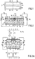
- FIGS 1 and 2 show a radiation-sensitive element 1 for use in the detector in accordance with the invention, Figure 1 being a plan view and Figure 2 a sectional view taken on the line II-II.
- the radiation-sensitive element 1 comprises a low-impedance substrate 2 on which an epitaxial layer 3 is provided. Further, the radiation-sensitive element is provided with mutually isolated rectifier junctions 5 (5A, 5B) on a substantially plane surface 4.
- the surface 4 of the element 1 is provided with p-type surface regions 6 (6A, 6B) which constitute rectifier junctions 5 (pn-junctions) with the epitaxial layer 3.
- the surface 4 of the element 1 is further covered with a passivating anti-reflection layer 7 of silicon oxide. In the layer 7 contact apertures 8 are formed for the contacts 9 (9A, 9B).
- Contact with the substrate 2 is provided by means of a contact metallisation 10 on the underside of the element.
- a voltage VA and VB respectively is applied between the contact metallisation 10 and the contacts 9A and 9B respectively, so that the rectifier junctions 5A and 5B are reverse-biassed.
- a depletion area is created near each rectifier junction 5 in the epitaxial layer 3 and the associated surface region 6, indicated by means of broken lines in Figure 2.
- the reference numeral 12 (12A, 12B) When the depletion regions extend into the epitaxial layer 3, these regions are indicated by the reference numeral 12 (12A, 12B).
- the electric field lines 13 represent the electric fields prevailing in the depletion regions 12.
- the distances between the subelements are so small that by applying a reverse voltage across the radiation-sensitive diode regions situated between adjacent subelements can be depleted by the depletion regions associated with the subelements.
- the electric field lines are deflected in such a way that as the electric field causes the charge carriers generated in the depletion region to migrate practically always to the corresponding pn-junction (the boundary between the depletion zones 12A and 12B bears the reference numeral 15). In this way they contribute to the photoelectric current generated in this pn-junction.
- the photoelectric currents generated in the pn-junctions 5A and 5B are indicated by I A and I B respectively.
- Figure 3a shows the variation of the currents I A and I B as function of the location of incidence x of the beam relative to the boundary 15 in the case that the reverse voltage VA and VB are equal to each other.
- the reference numeral 16 in this Figure represents a beam, for example a laser beam, which moves over the surface 4 of the semiconductor body When the beam 16 is situated at the location of point a the photoelectric current produced in the underlying pn-junction 5A is generated almost exclusively in a flat part of this junction parallel to the surface 4. This gives rise to a current I A of the value I o through this junction.
- the current I B through the adjacent pn-junction 5B is negligibly small.
- the distance between the surface 4 and the depletion region is shorter, so that less charge carriers are lost as a result of recombination and, moreover, less radiation is absorbed in the surface region 6A. In the case of a constant thickness of the layer 7 this would result in an additional contribution to the photoelectric current. However, between the surface regions 6A and 6B the layer 7 exhibits a thickened portion 36 which is selected in such a way that a larger amount of light is reflected at the location of this thickened portion to ensure that the current I A remains substantially the same.
- the current I A is produced mainly by charge carriers generated in the depletion region 12A to the left of the boundary 15, whilst the current I B is generated mainly by the charge carriers generated in the depletion region 12B. If V A and V B are not equal to each other, the depletion regions 12A and 12B are no longer symmetrical relative to the centre between the surface regions 6A and 6B, which means that the boundary 15 between the radiation-sensitive areas of the diodes is offset from the centre between the surface region 6A and 6B.
- Figures 3b and 3c respectively represent schematically the locations of the depletion regions 12A and 12B relative to the centre between the subelements 6A and 6B and the corresponding variations of the currents I A and I B .
- the position of the boundary 15 between the radiation-sensitive areas of the diodes constituted by the subelements 6 and the epitaxial layer 3 depends on the magnitude of the difference between the reverse voltage V A and V B .
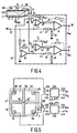
- FIG. 4 shows an embodiment of the device in accordance with the invention.
- the reference numeral 20 is a bias circuit for applying different reverse voltages V A and V B across the radiation-sensitive diodes of the radiation-sensitive element 1, which diodes are formed by the surface regions 6A and 6B and the epitaxial layer 3.
- the circuit 20 comprises an operational amplifier 21, whose inverting input is connected to the contact 9A of the surface region 6A.
- the non-inverting input of the operational amplifier 21 is connected to an input terminal 22.
- the output of the operational amplifier 21 is coupled to its inverting input via a resistor 23.
- the output of the amplifier 21 is connected to the inverting input 40 of a differential amplifier comprising an operational amplifier 24 and the resistors 25, 26, 27 and 28.
- the non-inverting input 41 of the differential amplifier is connected to the input terminal 22.
- the output of the operational amplifier 24 is connected to an output terminal 29.
- the contact 9B of the surface region 9B is connected to the inverting input of an operational amplifier 30, whose output is also connected to the inverting input via a resistor 31.
- the control signal PE on the input terminal 22 is inverted by means of an inverting amplifier comprising an operational amplifier 32 and resistors 33 and 34 and is subsequently applied to the non-inverting input of the operational amplifier 30 and to the non-inverting input 42 of a differential amplifier comprising an operational amplifier 35 and resistors 36, 37, 38 and 39.
- the output of the operational amplifier 30 is connected to the inverting input 43 of the differential amplifier comprising the operational amplifier 35.
- the output of the operational amplifier 35 is connected to the output terminal 44.
- the metallisation layer 10 is maintained at a constant voltage V BIAS by means of a voltage source (not shown).
- V BIAS voltage difference between the contact 9A and the metallisation layer 10
- V pe is the amplitude of the voltage of the control signal PE.
- the voltage on the non-inverting input of the operational amplifier 30 is -V pe , so that the voltage difference between the contact 9B and the metallisation layer 10 is equal to V BIAS +V pe .
- the boundary 15 between the radiation-sensitive areas of the diodes of the element 1 is shifted relative to the centre between the surface regions 6A and 6B by a distance determined by the control signal PE.
- a radiation beam is incident on the surface 4 photoelectric currents I A and I B are generated in the depletion regions 12A and 12B, the ratio between the currents I A and I B being determined by the location of incidence of the beam relative to the boundary 15.
- the currents I A and I B are converted into a voltage V ma and a voltage V mb respectively by means of operational amplifiers 21 and 30.
- the voltage V ma comprises a component determined by the control signal PE and a component determined by the current I A .
- the operational amplifier 24 which is arranged as a differential amplifier, a voltage V ma is produced on the output terminal 29, in which voltage the component determined by PE is eliminated, so that the voltage V ma is proportional to the current I A .
- the voltage V mb proportional to the current I B is generated on an output terminal 44.
- the radiation-sensitive element 1 described above together with the associated adjusting circuit 20 is mounted in an optical system it is possible after assembly to apply such a difference voltage between the contacts 9A and 9B by means of a control signal PE that the boundary 15 coincides with the centre of the location where the radiation beam is incident on the radiation-sensitive element.
- a radiation-sensitive element in an optoelectronic apparatus is aligned in that after assembly of this apparatus and correct adjustment of, for example, the focus of an objective system the position of an incident beam is measured by measuring the voltage difference between V ma and V mb .
- the voltage difference between the contacts 9A and 9B can be adjusted by varying the amplitude V pe of the control signal PE in such a way that the difference V ma -V mb indicates that I A is equal to I B (calibration point).
- V ma and V mb (V ma -V mb ) may subsequently be used as the control signal.
- a deviation ⁇ V m corresponds to a specific deviation of the location of incidence of the beam relative to the adjusted position of the boundary 15.
- FIG. 5 shows a detector in accordance with the invention, employing a quadrant diode 47.
- a diode comprises four surface regions 6F, 6G, 6H and 61 which are situated symmetrically about a common centre 50.
- the contacts 9F and 9G and the contacts 9H and 91 of the surface regions 6F and 6G and the surface regions 6H and 61 are connected to the input terminals of an adjusting circuit 20A and an adjusting circuit 20B of the type described in the foregoing. If the voltages across the radiation-sensitive diodes formed by the surface regions 6F, 6G, 6H and 61 together with the epitaxial layer 3 are equal to each other the photoelectric currents I F , I G I H and I I are substantially identical if the radiation beam is centred relative to the surface regions.
- a mismatch during assembly as a result of which the centre of the beam is incident at a location 50′ after adjustment of the optical system can be corrected as described hereinbefore by means of control signals PE1 and PE2 on the inputs 22A and 22B of the adjusting circuits 20A and 20B.
- the boundaries 15C and 15D between the radiation-sensitive areas are shifted in such a way that the point of intersection of the boundaries 15C and 15D coincides with the centre of the incident beam.
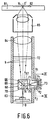
- a detector in accordance with the invention may be employed in, for example, a focus-error detection system as shown in Figure 6.
- Figure 6 shows a small part of a round disc-shaped record carrier 61 in radial cross-section.
- the radiation-reflecting information structure is situated on the upper side of the record carrier and comprises a multitude of information areas, not shown, which are arranged in information tracks 62.
- the information structure is scanned by a read beam b produced by a radiation source 63, for example a semiconductor diode laser.
- a lens 64 forms the diverging beam into a parallel beam of such a cross-section that the pupil of an objective system 65 is filled in an adequate manner.
- This objective system then forms a radiation spot V i of minimal dimensions on the information structure.
- the read beam is reflected from the information structure and, as the record carrier moves relative to the read beam, the reflected beam is time-modulated in conformity with the information recorded in the record carrier.
- a beam-separating prism 66 is arranged between the radiation source and the objective system. This prism may comprise two prismatic sections 67 and 68 between which a beam-separating layer 69 is interposed.
- the reference numerals 70 and 71 respectively denote the entrance face and the exit face of the prism 66.
- the layer 69 may be a semitransparent mirror.
- a polarisation-sensitive separating layer may be employed.
- a ⁇ /4 plate 72 should then be arranged between the objective system and the prism 66, A being the wavelength of the read beam b . This plate is traversed twice by the read beam and rotates the plane of polarisation of the beam through 90° in total.
- the beam emitted by the radiation source is then almost wholly transmitted by the prism, whilst the modulated beam is almost wholly reflected towards a radiation-sensitive detection system 73 which supplies a signal which is modulated in conformity with the information stored in the record carrier.
- a roof prism 74 is arranged on the exit face 71 of the beam-separating prism 66 and the radiation-sensitive detection system 73 comprises, for example, two radiation-sensitive devices as described with reference to Figures 1 and 2.
- Figure 7 which illustrates the principle of focus-error detection, these two devices bear the reference numerals 76 and 77.
- This Figure shows inter alia a sectional view of the semiconductor devices, taken on the line XI-XI in Figure 6 and shows schematically the auxiliary electronic circuit for adjusting the difference voltages for the purpose of zero setting.
- the refractive edge 75 of the prism 74 extends parallel to the optical axis 00′ in Figure 6 of the read unit.
- the roof prism splits the beam b into two subbeams b1 and b2 which are incident on the devices 76 and 77 respectively.
- Figure 6 illustrates the situation in which the read beam is focused exactly in the plane of the information structure.
- the read unit may be constructed in such a way that the focus of the reflected beam is situated exactly on the surface of the radiation-sensitive element 1 of the detector 76, 77.
- the distance between the centres of the radiation spots V1 and V2 formed on the detectors 76 and 77 by the beams b1 and b2 is a .
- the energy distribution within the subbeams b1 and b2 relative to the associated detectors changes, which may also be regarded as a displacement of the radiation spots V1 and V2 formed by the subbeams relative to the detectors. If the focus of the beam originating from the radiation source is situated above the plane of information structure, the beams b1 and b2 are moved inwards and the semiconductor zones 6A and 6D receive less radiation energy than the semiconductor zones 6B and 6C (the distance between the radiation spots V1′ and V2′ is then a ′).
- the focus of the beam emitted by the radiation source is situated below the plane of the information structure, the situation is reversed and the semiconductor zones 6B and 6C receive less radiation energy than the semiconductor zones 6A and 6D (the distance between the radiation spots V1 ⁇ and V2 ⁇ is then a ⁇ ).
- Figure 7 shows the positions of the radiation spots V1, V1′ and V1 ⁇ and V2, V2′ and V2 ⁇ shifted in a direction parallel to the boundary 15. It is to be noted that in reality the positions of the radiation spots in this direction do not change when the focussing changes.
- a correct adjustment of the boundaries 15A and 15B can be obtained by adjusting the distance between the boundaries and an adjustment which ensures that when the distance between the boundaries 15 remains the same these boundaries 15 are adjusted in such a way that they are situated symmetrically relative to the centre between the radiation spots formed on the detectors 76 and 77 by the beams b1 and b2.
- a symmetrical position of the boundaries relative to said centre between the radiation spots can be determined simply by means of the currents I A , I B , I C and I D . This is because the difference (I A +I C ) - (I B +I D ) is representative of the difference in distance between the centre between the boundaries 15A and 15B and the centre between the radiation spots.
- Figure 7 also shows a control system for automatically symmetrizing the boundaries 15A and 15B relative to the centre between the radiation spots on the basis of the difference (I A +I C ) - (I B +I D ).
- This control system comprises a section for determining a measure VE of the difference (I A +I C ) - (I B +I D ) formed by the bias circuits 20 and 20C; adder circuits 80 and 81 and a differential amplifier 83, and a section comprising the control circuit 84 for deriving from the signal VE the control signal PE for the adjusting circuits 20 and 20C, in such a way that the difference (I A +I C ) + (I B +I D ) is maintained equal to zero.
- the boundaries 15A and 15B are both shifted in a same direction and over substantially the same distance upon a change in amplitude of the control signal PE, so that the distance between the boundaries 15A and 15B is substantially independent of the control signal PE.
- the distance between the boundaries 15A and 15B can be adjusted by providing a voltage difference between the inputs 22 and 22C. This can be achieved, for example, by arranging in the connection between the output of the control circuit 84 and the control input 22C an adder circuit 88 which has one input connected to the output of the control circuit 84 and which has another input connected to a potentiometer 89 for adjusting the voltage difference between the control input 22 and 22C.
- the arrangement shown in Figure 7 comprises adder circuits 85 and 86 and a difference circuit 87 for generating a focus-error signal S f in the customary manner in conformity with the following relationship:
- the focus-error signal S f represents the distance between the boundaries 15A and 15B and the distance between the centres of the radiation spots V1 and V2, which difference is proportional to the focus error in the case of a correct adjustment of the distance between the boundaries 15A and 15B.
- the system can be adjusted by a correct adjustment of the distance between the boundaries 15A and 15B, for example by means of the potentiometer 89.
- the desired symmetry of the boundaries relative to the centre between the radiation spots is then obtained automatically. It is obvious that the correct distance between the boundaries can also be obtained in another manner, for example by means of the mechanical adjustment device described in the aforementioned Netherlands Patent Application 8202058.
- a detector in accordance with the invention may also be utilized in a focus-error detection system of the astigmatic type, for example as shown in Figure 8.
- the reference numeral 91 denotes a record carrier which is illuminated with a read beam 93 originating from a radiation source 94.
- An objective system 95 focusses the read beam to form a read spot V on the surface of the record carrier 1 on which the information structure is formed.
- the focal length of the auxiliary lens 96 is selected in such a way that the pupil of the objective system is filled adequately.
- the read beam is reflected from the record carrier and is then modulated in conformity with the information stored in a trackportion to be read.
- a beam splitter 98 is arranged in the radiation path.
- the beam splitter directs the modulated read beam to the detector 47 described in the foregoing, which detector is connected to a detection circuit 100 for deriving a focus-error signal S f .
- an astigmatic element 101 in the form of a cylindrical lens is arranged in the radiation path behind the beam splitter 98.
- an astigmatic system has two astigmatic focal lines which, viewed in an axial direction, occupy different positions and which extend perpendicularly to one another.
- the radiation-sensitive detector 47 is now arranged in a plane which, viewed along the optical axis, is situated between the lines 102 and 103, suitably at a location where the dimensions in two mutually perpendicular directions of the image spot associated with the read spot V are equal to an optimum extent in the case of a correct focussing.
- the detector 47 In order to enable the shape of the image spot, V′ and hence the degree of focussing to be determined, use is made of the detector 47 described with reference to Figure 5, which detector comprises four subdetectors arranged in the four quadrants of an X-Y coordinate system.
- Figures 9a, 9b and 9c show the detector 47 in views taken on the line 92, 92′ in Figure 8, the various shapes of the image spot V′ being projected thereon for different values of the distance between the objective system and the plane of the tracks.
- the X-axis and Y-axis extend at an angle of 45° to the axis 105 of the cylindrical lens, i.e to the astigmatic focal lines 102 and 103, whilst the X-axis extends parallel to the effective track direction.
- Figure 9a illustrates the situation in which the distance between the objective system and the plane of the tracks is correct. If this distance is too large, the focal lines 102 and 103 are situated closer to the cylindrical lens 101. The detector 47 is then situated closer to the focal line 103 than to the focal line 102. The image spot V′ then has a shape as shown in Figure 9b. If the distance between the objective system and the plane of the tracks is too small the focal lines 102 and 103 are situated farther from the cylindrical lens and the focal line 102 is situated closer to the detector 47 than the focal line 103. The image spot V′ then has a shape as shown in Figure 9c.
- the detection circuit comprises an automatic bias circuit (see Figure 10) which shifts the boundaries 15C and 15D in such a way that the centre of the radiation spot V' coincides with the intersection of the boundaries 15C and 15D.
- This circuit comprises a first section for establishing the voltage difference between the contacts 9F and 9G and a second section for establishing the voltage difference between the contacts 9H and 91.
- the first section comprises the adjusting circuit 20A, a differential amplifier 120 for deriving a measure VE1 of the difference between the currents I F and I G from the output signals Vm f and V mg , and a control circuit 121 for deriving from the measure VE1 a signal PE1 applied to the input 22A of the adjusting circuit 20A, so as to minimize the difference between I F and I G .
- the second section comprises the adjusting circuit 20B, a differential amplifier 122 for deriving a measure VE2 of the difference between the currents I H and I I from the output signals V mh and V mi , and a control circuit 123 for deriving a signal PE2 applied to the input 22B of the circuit 20B so as to minimize the difference between the currents I H and I I .
- the detector 47 is adjusted fully automatically in such a way that the difference between I F and I G and the difference between I H and I I is minimized, which means that the intersection between the boundaries 15C and 15D coincides with the centre of the incident beam.
- any detector enabling the boundary between the radiation-sensitive areas of the individual diodes to be adjusted electronically is, in principle, suitable for use in the automatically adjustable focus-error detection system.
- An example of a suitable detector is described in the Netherlands Patent Application No. 8501489.
- the focus-error detection systems described herein do not utilize special properties of the optical information structure or of the surface on which focussing is effected. Therefore, the focus-error detection system can be utilized in various devices in which a very accurate focussing is required, for example in microscopes.
Landscapes
- Physics & Mathematics (AREA)
- Optics & Photonics (AREA)
- Optical Recording Or Reproduction (AREA)
- Light Receiving Elements (AREA)
- Optical Head (AREA)
- Automatic Focus Adjustment (AREA)
- Measurement Of Radiation (AREA)
Claims (5)
- Lageempfindlicher Strahlungsdetektor mit einem strahlungsempfindlichen Halbleiterelement mit einem Halbleiterkörper (1), der auf einer nahezu ebenen Oberfläche (2, 3) mit mindestens zwei Subelementen (6A, 6B) versehen ist, die mit den angrenzenden Teilen des Halbleiterkörpers strahlungsempfindliche Dioden bilden, wobei der Abstand zwischen den Subelementen klein genug ist, um durch die zu den Subelementen gehörenden Verarmungsgebiete (12A, 12B) ein vollständiges Verarmen der Zone des Halbleiterkörpers zwischen den Subelementen durch Anlegen einer Sperrspannung (VA, VB) an die Dioden zu ermöglichen, so daß Ladungstransport zwischen den Subelementen verhindert wird, eine Schaltung (20) um eine Sperrspannung an die strahlungsempfindlichen Dioden zu legen und die durch die Strahlung in den von den Verarmungsgebieten gebildeten strahlungsempfindlichen Gebieten der Dioden erzeugten Photoströme (IA, IB) zu detektieren, dadurch gekennzeichnet, daß die Schaltung (20) Mittel umfaßt, um in Abhängigkeit von einem Steuersignal (PE) verschiedene Sperrspannungen (VA, VB) an die Dioden zu legen, um die Grenze zwischen den strahlungsempfindlichen Gebieten der Dioden einzustellen.
- Detektor nach Anspruch 1, dadurch gekennzeichnet, daß die Schaltung (20) mindestens einen rückgekoppelten Differenzverstärker (21) umfaßt, der einen der durch die Strahlung erzeugten Photoströme (IA) in ein Meßsignal umwandelt, wofür eines der Subelemente (6B) mit dem invertierenden Eingang (-) des Differenzverstärkers (21) gekoppelt ist, um den umzuwandelnden Strom diesem Eingang zuzuführen, wobei die Schaltung außerdem Mittel (22) umfaßt, um eine Sperrspannung, deren Amplitude von dem Steuersignal (PE) am nicht-invertierenden Eingang (+) des Differenzverstärkers (21) abhängt, an die strahlungsempfindlichen Dioden zu legen.
- Detektor nach Anspruch 2, dadurch gekennzeichnet, daß die Schaltung einen zweiten Differenzverstärker (24) zum Erzeugen eines Meßsignals (Vms) umfaßt, das ein Maß für die Differenz zwischen der Ausgangsspannung des ersten Differenzverstärkers (21) und der Steuerspannung (PE) am nicht-invertierenden Eingang (+) des ersten Differenzverstärkers (21) ist, wofür der invertierende Eingang (-) des zweiten Differenzverstärkers mit dem Ausgang (40) des ersten Differenzverstärkers (21) gekoppelt ist und die Schaltung Mittel (27, 28) umfaßt, um eine zur Steuerspannung (PE) proportionale Spannung an den nicht-invertierenden Eingang (+) des zweiten Differenzverstärkers (24) zu legen.
- Optoelektronisches Fokusfehlerdetektionssystem zum Detektieren einer Abweichung zwischen einer reflektierenden Detektionsfläche (61) und einer Fokussierungsebene eines Objektivsystems (65) zum Lenken eines Strahlungsbündels zu der Detektionsfläche, wobei das Detektionssystem folgendes umfaßt:(i) einen ersten (76) und einen zweiten (77) lageempfindlichen Strahlungsdetektor nach Anspruch 1, jeder mit- einem strahlungsempfindlichen Halbleiterelement mit mindestens zwei Subelementen (6A,B; 6C,D) von nahezu rechteckiger Form, die nahezu parallel zueinander auf der Oberfläche eines Halbleiterkörpers angeordnet sind, und- einer ersten Schaltung (20, 20C) zum Anlegen von Sperrspannungen an die Dioden;(ii) ein Strahlteilerelement (74) zum Aufspalten des von der Detektionsfläche reflektierten Strahlungsbündels (b) in ein erstes und ein zweites Teilbündel, die in den Grenzgebieten der aneinandergrenzenden Dioden der Halbleiterelemente auf das erste bzw. zweite strahlungsempfindliche Halbleiterelement einfallen, wobei diese Halbleiterelemente so angeordnet sind, daß die nahezu rechteckigen Subelemente senkrecht zu der die Einfallspunkte des ersten und des zweiten Teilbündels verbindenden Linie senkrecht stehen;(iii) eine zweite Schaltung (85, 86, 87) zum Ableiten eines Fokusfehlersignals (Sf) aus den in den Dioden von den Teilbündeln erzeugten Photoströmen;wobei
die ersten Schaltungen (20; 206) Einstellmittel zum Einstellen der Grenzen zwischen den strahlungsempfindlichen Gebieten der Dioden umfassen, durch Erzeugen unterschiedlicher Sperrspannungen an den Dioden des ersten Halbleiterelements und den Dioden des zweiten Halbleiterelements in Abhängigkeit von einem Steuersignal (PE), wobei das Detektionssystem weiterhin eine Steuereinrichtung (80, 81, 83, 84) zum Ableiten der Steuersignale für die grenzeinstellenden Mittel aus den so erzeugten Photoströmen umfaßt, in der Weise, daß die Summe aus dem in derjenigen Diode des ersten Halbleiterelements, die weiter von der Mitte zwischen den Einfallsorten der Strahlenbündel gelegen ist, erzeugten Photostrom und dem in jener Diode des zweiten Halbleiterelements, das nahe der genannten Mitte gelegen ist, erzeugten Photostrom nahezu gleich der Summe aus den in den beiden anderen Dioden erzeugten Photoströmen bleibt. - Optoelektronisches Fokusfehlerdetektionssystem zum Detektieren einer Abweichung zwischen einer reflektierenden Detektionsfläche (41) und einer Fokussierungsebene eines Objektivsystems (45) zum Lenken eines Strahlungsbündels zu der Detektionsfläche, wobei das Detektionssystem folgendes umfaßt:(i) einen lageempfindlichen Strahlungsdetektor nach Anspruch 1, mit- einem strahlungsempfindlichen Halbleiterelement mit vier Subelementen, die in bezug auf eine gemeinsame Mitte auf einer Oberfläche eines Halbleiterkörpers symmetrisch angeordnet sind, und- einer ersten Schaltung zum Anlegen von Sperrspannungen an die Dioden;(ii) ein optisches System (98, 101, 102) zum Lenken des von der Detektionsfläche reflektierten Strahlungsbündels zu den strahlungsempfindlichen Dioden des Halbleiterelements;(iii) ein im optischen Weg zwischen der Detektionsfläche und dem Halbleiterelement angeordnetes astigmatisches Element (101); und(iv) eine zweite Schaltung (124, 125, 126) zum Ableiten eines Fokusfehlersignals (Sf) aus den in den Dioden erzeugten Photoströmen;wobei die erste Schaltung Mittel (20A, 20B) zum Einstellen der Grenzen zwischen den strahlungsempfindlichen Dioden umfaßt, durch Erzeugen unterschiedlicher Sperrspannungen an diagonal gegenüberliegenden Dioden in Abhängigkeit von Steuersignalen (22A, 22B), wobei das Detektionssystem weiterhin eine Steuereinrichtung (120, 121, 122, 123) zum Ableiten der Steuersignale in Abhängigkeit von den in den Dioden erzeugten Photoströmen umfaßt, in der Weise, daß die in diagonal gegenüberliegenden Dioden erzeugten Photoströme nahezu gleich zueinander bleiben.
Applications Claiming Priority (2)
| Application Number | Priority Date | Filing Date | Title |
|---|---|---|---|
| NL8601719 | 1986-07-02 | ||
| NL8601719A NL8601719A (nl) | 1986-07-02 | 1986-07-02 | Electronisch instelbare positiegevoelige stralingsdetector, focusfoutdetectiestelsel voorzien van een dergelijke stralingsdetector, en optische lees- en/of schrijfinrichting voorzien van een dergelijk focusfoutdetectiestelsel. |
Publications (3)
| Publication Number | Publication Date |
|---|---|
| EP0251402A2 EP0251402A2 (de) | 1988-01-07 |
| EP0251402A3 EP0251402A3 (en) | 1988-03-30 |
| EP0251402B1 true EP0251402B1 (de) | 1994-09-14 |
Family
ID=19848253
Family Applications (1)
| Application Number | Title | Priority Date | Filing Date |
|---|---|---|---|
| EP87201192A Expired - Lifetime EP0251402B1 (de) | 1986-07-02 | 1987-06-23 | Lageempfindlicher, elektronisch einstellbarer Strahlungsdetektor, Detektionssystem von Fokusfehlern mit diesem Detektor und optische Lese- und/oder Schreibanordnung mit diesem System |
Country Status (8)
| Country | Link |
|---|---|
| US (1) | US4810871A (de) |
| EP (1) | EP0251402B1 (de) |
| JP (1) | JPS6328077A (de) |
| KR (1) | KR880002279A (de) |
| CN (1) | CN1013721B (de) |
| CA (1) | CA1273717A (de) |
| DE (1) | DE3750528T2 (de) |
| NL (1) | NL8601719A (de) |
Families Citing this family (12)
| Publication number | Priority date | Publication date | Assignee | Title |
|---|---|---|---|---|
| US4916306A (en) * | 1988-07-14 | 1990-04-10 | Tektronix | Device for detecting spatial variation in the intensity of electromagnetic radiation |
| US4928003A (en) * | 1988-07-15 | 1990-05-22 | Tektronix, Inc. | Charge-coupled device for detecting spatial variation in the intensity of electromagnetic radiation |
| JPH0648575Y2 (ja) * | 1988-09-13 | 1994-12-12 | パイオニア株式会社 | 光検出器 |
| NL8901400A (nl) * | 1989-06-02 | 1991-01-02 | Philips Nv | Halfgeleiderinrichting met een stralingsgevoelig element. |
| NL8901629A (nl) * | 1989-06-28 | 1991-01-16 | Philips Nv | Stralingsgevoelige halfgeleiderinrichting en uitlees- of schrijfeenheid bevattende een dergelijke stralingsgevoelige halfgeleiderinrichting. |
| JPH04195938A (ja) * | 1990-11-28 | 1992-07-15 | Olympus Optical Co Ltd | 光学的情報記録再生装置 |
| US5530543A (en) * | 1994-07-06 | 1996-06-25 | Optra, Inc. | Detector array for use in interferometric metrology systems |
| IT1312204B1 (it) * | 1999-04-22 | 2002-04-09 | Electronic Systems Spa | Dispositivo per la misura dello spessore di materiale in foglio mentre questo avanza e relativo metodo di misurazione |
| KR100432660B1 (ko) * | 2001-08-17 | 2004-05-22 | 삼성전기주식회사 | 광픽업 장치 |
| US20030034540A1 (en) * | 2001-08-20 | 2003-02-20 | Em Microelectronic-Marin Sa | Photodetector, photodetecting device and method for controlling the sensitivity profile of a photodetector |
| DE102006013461B3 (de) * | 2006-03-23 | 2007-11-15 | Prüftechnik Dieter Busch AG | Photodetektoranordnung, Messanordnung mit einer Photodetektoranordnung und Verfahren zum Betrieb einer Messanordnung |
| DE102006013460B3 (de) * | 2006-03-23 | 2007-11-08 | Prüftechnik Dieter Busch AG | Photodetektoranordnung, Messanordnung mit einer Photodetektoranordnung und Verfahren zum Betrieb einer Messanordnung |
Citations (1)
| Publication number | Priority date | Publication date | Assignee | Title |
|---|---|---|---|---|
| EP0206363A1 (de) * | 1985-05-24 | 1986-12-30 | Koninklijke Philips Electronics N.V. | Lageempfindlicher Strahlungsdetektor |
Family Cites Families (8)
| Publication number | Priority date | Publication date | Assignee | Title |
|---|---|---|---|---|
| US3742223A (en) * | 1970-05-25 | 1973-06-26 | Mc Donnell Douglas Corp | Wide angle lateral photo-detector means |
| US3704376A (en) * | 1971-05-24 | 1972-11-28 | Inventors & Investors Inc | Photo-electric junction field-effect sensors |
| US3870887A (en) * | 1973-10-10 | 1975-03-11 | Mc Donnell Douglas Corp | Optical image position indicator means using time and phase delay sensing |
| NL7703077A (nl) * | 1977-03-22 | 1978-09-26 | Philips Nv | Inrichting voor het uitlezen van een stralings- reflekterende registratiedrager. |
| JPS6038771B2 (ja) * | 1978-06-19 | 1985-09-03 | パイオニア株式会社 | 光学式情報読取装置のサ−ボ装置 |
| NL8003906A (nl) * | 1980-07-07 | 1982-02-01 | Philips Nv | Stralingsgevoelige halfgeleiderinrichting. |
| US4366377A (en) * | 1980-09-29 | 1982-12-28 | Mcdonnell Douglas Corporation | Dual sensitivity optical sensor |
| NL187374C (nl) * | 1981-07-10 | 1991-09-02 | Philips Nv | Inrichting voor het detecteren van straling. |
-
1986
- 1986-07-02 NL NL8601719A patent/NL8601719A/nl not_active Application Discontinuation
- 1986-11-10 US US06/929,135 patent/US4810871A/en not_active Expired - Fee Related
-
1987
- 1987-06-23 EP EP87201192A patent/EP0251402B1/de not_active Expired - Lifetime
- 1987-06-23 DE DE3750528T patent/DE3750528T2/de not_active Expired - Fee Related
- 1987-06-25 CA CA000540610A patent/CA1273717A/en not_active Expired - Lifetime
- 1987-06-29 CN CN87104584A patent/CN1013721B/zh not_active Expired
- 1987-06-29 KR KR1019870006608A patent/KR880002279A/ko not_active Ceased
- 1987-07-02 JP JP62164109A patent/JPS6328077A/ja active Pending
Patent Citations (1)
| Publication number | Priority date | Publication date | Assignee | Title |
|---|---|---|---|---|
| EP0206363A1 (de) * | 1985-05-24 | 1986-12-30 | Koninklijke Philips Electronics N.V. | Lageempfindlicher Strahlungsdetektor |
Also Published As
| Publication number | Publication date |
|---|---|
| KR880002279A (ko) | 1988-04-30 |
| CN1013721B (zh) | 1991-08-28 |
| EP0251402A3 (en) | 1988-03-30 |
| JPS6328077A (ja) | 1988-02-05 |
| NL8601719A (nl) | 1988-02-01 |
| DE3750528D1 (de) | 1994-10-20 |
| CA1273717A (en) | 1990-09-04 |
| EP0251402A2 (de) | 1988-01-07 |
| DE3750528T2 (de) | 1995-04-06 |
| CN87104584A (zh) | 1988-01-13 |
| US4810871A (en) | 1989-03-07 |
Similar Documents
| Publication | Publication Date | Title |
|---|---|---|
| US4749849A (en) | Device for determining the position of a radiation beam | |
| KR880001707B1 (ko) | 광전자 집속에러 검출장치 | |
| EP0219908B1 (de) | Gerät zur optischen Abtastung einer Informationsebene | |
| EP0177108B1 (de) | Optoelektronisches Detektionssystem für Fokussierfehler | |
| EP0251402B1 (de) | Lageempfindlicher, elektronisch einstellbarer Strahlungsdetektor, Detektionssystem von Fokusfehlern mit diesem Detektor und optische Lese- und/oder Schreibanordnung mit diesem System | |
| GB2059057A (en) | Photo-electric focussing error detection | |
| EP0044074A1 (de) | Brennpunktdetektor | |
| EP0512616B1 (de) | Optische Abtastvorrichtung | |
| PL133015B1 (en) | Opto-electronic focusing error detection system | |
| US4135207A (en) | Apparatus for reading an optical radiation-reflecting record carrier including a narrow focus control beam | |
| US3742223A (en) | Wide angle lateral photo-detector means | |
| US5029261A (en) | Apparatus for detecting position of light beam on object surface by comparing detection beams split near focal point | |
| CA1116294A (en) | Apparatus for reading an optical radiation-reflecting record carrier | |
| US5500846A (en) | Radiation source-detection unit employing a grating having two grating structures, and a device including that unit | |
| JPH079708B2 (ja) | 光デイスクヘツドのフオ−カスずれ検出装置 | |
| US4888491A (en) | Device for measuring angular deviation of flat plate | |
| EP0475523B1 (de) | Vorrichtung zum Abtasten einer Informationsfläche mit optischer Strahlung | |
| US4987461A (en) | High position resolution sensor with rectifying contacts | |
| EP0605929B1 (de) | Vorrichtung zur optischen Abtastung einer Fläche | |
| JPH0654231B2 (ja) | 非接触変位計 | |
| US4270045A (en) | Apparatus for reading an optical radiation-reflecting information carrier for controlling focus | |
| JP2552660B2 (ja) | フオ−カス誤差検出装置 | |
| KR830000430B1 (ko) | 광학적 방사선 정보담체(Carrier)의 독취장치 | |
| JPS6032136A (ja) | 光学ヘッド |
Legal Events
| Date | Code | Title | Description |
|---|---|---|---|
| PUAI | Public reference made under article 153(3) epc to a published international application that has entered the european phase |
Free format text: ORIGINAL CODE: 0009012 |
|
| AK | Designated contracting states |
Kind code of ref document: A2 Designated state(s): BE DE FR GB IT NL |
|
| PUAL | Search report despatched |
Free format text: ORIGINAL CODE: 0009013 |
|
| AK | Designated contracting states |
Kind code of ref document: A3 Designated state(s): BE DE FR GB IT NL |
|
| 17P | Request for examination filed |
Effective date: 19880920 |
|
| 17Q | First examination report despatched |
Effective date: 19900820 |
|
| GRAA | (expected) grant |
Free format text: ORIGINAL CODE: 0009210 |
|
| AK | Designated contracting states |
Kind code of ref document: B1 Designated state(s): BE DE FR GB IT NL |
|
| PG25 | Lapsed in a contracting state [announced via postgrant information from national office to epo] |
Ref country code: IT Free format text: LAPSE BECAUSE OF FAILURE TO SUBMIT A TRANSLATION OF THE DESCRIPTION OR TO PAY THE FEE WITHIN THE PRE;WARNING: LAPSES OF ITALIAN PATENTS WITH EFFECTIVE DATE BEFORE 2007 MAY HAVE OCCURRED AT ANY TIME BEFORE 2007. THE CORRECT EFFECTIVE DATE MAY BE DIFFERENT FROM THE ONE RECORDED.SCRIBED TIME-LIMIT Effective date: 19940914 Ref country code: BE Effective date: 19940914 Ref country code: NL Effective date: 19940914 |
|
| REF | Corresponds to: |
Ref document number: 3750528 Country of ref document: DE Date of ref document: 19941020 |
|
| ET | Fr: translation filed | ||
| NLV1 | Nl: lapsed or annulled due to failure to fulfill the requirements of art. 29p and 29m of the patents act | ||
| PG25 | Lapsed in a contracting state [announced via postgrant information from national office to epo] |
Ref country code: GB Effective date: 19950623 |
|
| PLBE | No opposition filed within time limit |
Free format text: ORIGINAL CODE: 0009261 |
|
| STAA | Information on the status of an ep patent application or granted ep patent |
Free format text: STATUS: NO OPPOSITION FILED WITHIN TIME LIMIT |
|
| 26N | No opposition filed | ||
| GBPC | Gb: european patent ceased through non-payment of renewal fee |
Effective date: 19950623 |
|
| PG25 | Lapsed in a contracting state [announced via postgrant information from national office to epo] |
Ref country code: FR Effective date: 19960229 |
|
| PG25 | Lapsed in a contracting state [announced via postgrant information from national office to epo] |
Ref country code: DE Effective date: 19960301 |
|
| REG | Reference to a national code |
Ref country code: FR Ref legal event code: ST |