EP0249311B1 - Liquid crystal optical devices - Google Patents
Liquid crystal optical devices Download PDFInfo
- Publication number
- EP0249311B1 EP0249311B1 EP87302816A EP87302816A EP0249311B1 EP 0249311 B1 EP0249311 B1 EP 0249311B1 EP 87302816 A EP87302816 A EP 87302816A EP 87302816 A EP87302816 A EP 87302816A EP 0249311 B1 EP0249311 B1 EP 0249311B1
- Authority
- EP
- European Patent Office
- Prior art keywords
- liquid crystal
- crystal device
- major
- optical
- crystal material
- Prior art date
- Legal status (The legal status is an assumption and is not a legal conclusion. Google has not performed a legal analysis and makes no representation as to the accuracy of the status listed.)
- Expired - Lifetime
Links
Images


Classifications
-
- G—PHYSICS
- G02—OPTICS
- G02F—OPTICAL DEVICES OR ARRANGEMENTS FOR THE CONTROL OF LIGHT BY MODIFICATION OF THE OPTICAL PROPERTIES OF THE MEDIA OF THE ELEMENTS INVOLVED THEREIN; NON-LINEAR OPTICS; FREQUENCY-CHANGING OF LIGHT; OPTICAL LOGIC ELEMENTS; OPTICAL ANALOGUE/DIGITAL CONVERTERS
- G02F1/00—Devices or arrangements for the control of the intensity, colour, phase, polarisation or direction of light arriving from an independent light source, e.g. switching, gating or modulating; Non-linear optics
- G02F1/01—Devices or arrangements for the control of the intensity, colour, phase, polarisation or direction of light arriving from an independent light source, e.g. switching, gating or modulating; Non-linear optics for the control of the intensity, phase, polarisation or colour
- G02F1/13—Devices or arrangements for the control of the intensity, colour, phase, polarisation or direction of light arriving from an independent light source, e.g. switching, gating or modulating; Non-linear optics for the control of the intensity, phase, polarisation or colour based on liquid crystals, e.g. single liquid crystal display cells
- G02F1/132—Thermal activation of liquid crystals exhibiting a thermo-optic effect
-
- G—PHYSICS
- G02—OPTICS
- G02F—OPTICAL DEVICES OR ARRANGEMENTS FOR THE CONTROL OF LIGHT BY MODIFICATION OF THE OPTICAL PROPERTIES OF THE MEDIA OF THE ELEMENTS INVOLVED THEREIN; NON-LINEAR OPTICS; FREQUENCY-CHANGING OF LIGHT; OPTICAL LOGIC ELEMENTS; OPTICAL ANALOGUE/DIGITAL CONVERTERS
- G02F1/00—Devices or arrangements for the control of the intensity, colour, phase, polarisation or direction of light arriving from an independent light source, e.g. switching, gating or modulating; Non-linear optics
- G02F1/01—Devices or arrangements for the control of the intensity, colour, phase, polarisation or direction of light arriving from an independent light source, e.g. switching, gating or modulating; Non-linear optics for the control of the intensity, phase, polarisation or colour
- G02F1/13—Devices or arrangements for the control of the intensity, colour, phase, polarisation or direction of light arriving from an independent light source, e.g. switching, gating or modulating; Non-linear optics for the control of the intensity, phase, polarisation or colour based on liquid crystals, e.g. single liquid crystal display cells
- G02F1/1326—Liquid crystal optical waveguides or liquid crystal cells specially adapted for gating or modulating between optical waveguides
-
- G—PHYSICS
- G02—OPTICS
- G02F—OPTICAL DEVICES OR ARRANGEMENTS FOR THE CONTROL OF LIGHT BY MODIFICATION OF THE OPTICAL PROPERTIES OF THE MEDIA OF THE ELEMENTS INVOLVED THEREIN; NON-LINEAR OPTICS; FREQUENCY-CHANGING OF LIGHT; OPTICAL LOGIC ELEMENTS; OPTICAL ANALOGUE/DIGITAL CONVERTERS
- G02F1/00—Devices or arrangements for the control of the intensity, colour, phase, polarisation or direction of light arriving from an independent light source, e.g. switching, gating or modulating; Non-linear optics
- G02F1/01—Devices or arrangements for the control of the intensity, colour, phase, polarisation or direction of light arriving from an independent light source, e.g. switching, gating or modulating; Non-linear optics for the control of the intensity, phase, polarisation or colour
- G02F1/13—Devices or arrangements for the control of the intensity, colour, phase, polarisation or direction of light arriving from an independent light source, e.g. switching, gating or modulating; Non-linear optics for the control of the intensity, phase, polarisation or colour based on liquid crystals, e.g. single liquid crystal display cells
- G02F1/137—Devices or arrangements for the control of the intensity, colour, phase, polarisation or direction of light arriving from an independent light source, e.g. switching, gating or modulating; Non-linear optics for the control of the intensity, phase, polarisation or colour based on liquid crystals, e.g. single liquid crystal display cells characterised by the electro-optical or magneto-optical effect, e.g. field-induced phase transition, orientation effect, guest-host interaction or dynamic scattering
- G02F1/13781—Devices or arrangements for the control of the intensity, colour, phase, polarisation or direction of light arriving from an independent light source, e.g. switching, gating or modulating; Non-linear optics for the control of the intensity, phase, polarisation or colour based on liquid crystals, e.g. single liquid crystal display cells characterised by the electro-optical or magneto-optical effect, e.g. field-induced phase transition, orientation effect, guest-host interaction or dynamic scattering using smectic liquid crystals
-
- G—PHYSICS
- G02—OPTICS
- G02F—OPTICAL DEVICES OR ARRANGEMENTS FOR THE CONTROL OF LIGHT BY MODIFICATION OF THE OPTICAL PROPERTIES OF THE MEDIA OF THE ELEMENTS INVOLVED THEREIN; NON-LINEAR OPTICS; FREQUENCY-CHANGING OF LIGHT; OPTICAL LOGIC ELEMENTS; OPTICAL ANALOGUE/DIGITAL CONVERTERS
- G02F1/00—Devices or arrangements for the control of the intensity, colour, phase, polarisation or direction of light arriving from an independent light source, e.g. switching, gating or modulating; Non-linear optics
- G02F1/29—Devices or arrangements for the control of the intensity, colour, phase, polarisation or direction of light arriving from an independent light source, e.g. switching, gating or modulating; Non-linear optics for the control of the position or the direction of light beams, i.e. deflection
- G02F1/292—Devices or arrangements for the control of the intensity, colour, phase, polarisation or direction of light arriving from an independent light source, e.g. switching, gating or modulating; Non-linear optics for the control of the position or the direction of light beams, i.e. deflection by controlled diffraction or phased-array beam steering
Definitions
- the switch uses double interaction with the single layer to switch unpolarised light from one multinode optical fiber to another in response to a change in operating voltage.
- the liquid crystal material may be dyed to improve the absorption of energy from a laser or other light source used to heat the material to change its state.
- the dye should be chosen so as not to attenuate the light to be propoagated through the resulting device.
- a red dye may be used if the light to be propagated is red from a helium-neon laser, for example, and in this instance an argon ion laser producing blue light which is strongly absorbed by the dye may be used to heat the material instead of the helium-neon laser as mentioned earlier.
Landscapes
- Physics & Mathematics (AREA)
- Nonlinear Science (AREA)
- General Physics & Mathematics (AREA)
- Optics & Photonics (AREA)
- Chemical & Material Sciences (AREA)
- Crystallography & Structural Chemistry (AREA)
- Liquid Crystal (AREA)
- Optical Integrated Circuits (AREA)
- Glass Compositions (AREA)
Abstract
Description
- The present invention relates to optical devices using liquid crystal material. Liquid crystal materials are liquids which exhibit the long range molecular order characteristic of crystals although they are in the liquid state. They display marked changes in their optical properties with changes of their temperature or in response to an applied electric field. There are three predominant meso-phases which may exist between the solid and isotropic liquid states and these are, in the order in which they generally occur with ascending temperature, the smectic, nematic and cholesteric phases. Not all liquid crystal materials exhibit all phases. In a common application of liquid crystal materials they are used to produce display devices for electronic calculators and portable computers. In additions two-dimensional arrays of liquid crystal elements have been used to produce displays of images and also of television pictures.
- With the advent of optical waveguides to convey information signals a need has arisen for optical devices which can be controlled electrically. To this end an attempt has been made to produce a light channel using liquid crystal material in the nematic phase. However, it was found that the channel imposed a loss of about 30 dB/cm on the light propagated through it which was considered to be unacceptable. It has also been noted that the propagation loss of light through an aligned smectic A liquid crystal material is much lower at about 2 dB/cm, but proposals have been made for display devices using such material in light scattering and transparent forms.
- A paper by R.A. Soref et al in Optics Letters vol, no. 4, April 1980 pp. 147-149 entitled "Total Switching of unpolarised fiber light with a four-part electro-optic liquid cystal device" discloses a liquid-crystal switch with a single layer of nematic liquid cystal material interposed between two major bounding surfaces.
- The switch uses double interaction with the single layer to switch unpolarised light from one multinode optical fiber to another in response to a change in operating voltage.
- It is an object of the present invention to provide optical devices using liquid crystal material in the smectic phase.
- The object is solved, according to the invention, with the features of
apparatus claim 1 and method claim 16. - The present invention provides a liquid crystal device having a smectic A phase liquid crystal material in only two transparent states of differing molecular orientation, which states present differing respective refractive indices to polarised light transmitted through the device, the smectic A phase liquid crystal material in one transparent state having a molecular orientation substantially orthogonal to the material in the other transparent state, and the liquid crystal material being interposed between two major bounding surfaces, the orientation in one state being homogenous and substantially parallel to the major bounding surfaces, and the orientation in the other state being homeotropic and substantially orthogonal to the major bounding surfaces.
- In a preferred embodiment, a part of the material in one state forms an optical waveguide for polarised light having a plane of polarisation related to the molecular orientation of said part, and wherein a part of the material in the other state abuts the part in the one state to form a boundary of the optical waveguide.
- Optical waveguides may be connected to such a structure by being brought to the periphery of the cell containing the material and means, for example a laser, may be used to effect the change in state of the material along a line joining a point on the periphery of the cell where the guide selected as the output waveguide meets it. Alternatively, the waveguides joining the liquid crystal material may be used to link from and/or to waveguides embodied in the major walls of the cell and produced, for example, by ion exchange. The waveguides written into the liquid crystal material may be arranged as field couplers, ring resonators, or other waveguide circuit components.
- The invention also provides an optical component comprising a liquid crystal device as defined above, wherein the shapes of the parts in the two states are arranged to produce a required effect on polarised light transmitted through the device.
- The invention further provides an adjustable optical component comprising a liquid crystal device as defined above, wherein the boundary between the parts in the different states determines the effect of the device on polarised light transmitted through it, and wherein the position of the boundary is changeable by selective alteration of the states of at least some of the liquid crystal material, thereby to alter the effect of the component on the light transmitted through it.
- The two states of the liquid crystal material have different molecular orientation and by virtue of the birefringence of the material it can present different refractive indices to light polarised in a particular plane. The two molecular orientations may be orthogonal and the plane of polarisation of the light may be chosen to be parallel to the molecules of the material in one state and perpendicular to the molecules of the material in the other state.
- The two states may both have homogeneous alignment of the molecules, that is to say the molecules are parallel to the major bounding planes of the cell containing the material, and preferably the molecules in one state are perpendicular to the molecules in the other state. Light polarised parallel to the major bounding planes and passing through the liquid crystal material between the major bounding planes will encounter a higher refractive index where it meets the molecules of the material transversely than where it meets the molecules end on. At least, this is the effect for most liquid crystal materials, although there are materials for which the effect is reversed. By making the region of higher refractive index a passage bounded by regions of lower refractive index, the first-mentioned region will act as a guide for the polarised light. Other configurations of the regions can be produced so as to provide other optical components.
- In another example one of the states may have homogeneous alignment of the molecules and the other state may have homeotropic alignment of the molecules in which the molecules stand perpendicular to the major bounding planes. In this case light passing through the material between the major bounding planes may be polarised either parallel or perpendicular to the major bounding planes and will encounter different refractive indices in the material, depending on the alignment of the molecules relative to plane of polarisation of the light as described above and components having adjustable optical properties may be constructed, the adjustment being effected by changing the state of some of the liquid crystal material.
- Instead of being directed through the material between the major bounding planes, the polarised light may be directed roughly normally to the major bounding planes, and the regions of differing refractive indices may be in closely spaced parallel lines thereby providing a diffraction grating, so that the light is diffracted and a part of it leaves the component in a predetermined direction. The spacing of the lines of the grating and their orientation can be altered by converting all the liquid crystal material to the same state and then regenerating the regions of different refractive index as lines in the orientation and with the spacing required.
- Liquid crystal material in the smectic A phase is highly viscous with the molecules aligned in parallel, and in each plane the long axes of the molecules are perpendicular to the plane. As mentioned above, smectic A liquid crystal material may be arranged to have two alignments relative to the major bounding planes of the cello homogeneous and homeotropic. In homogeneous alignment the long axes of the molecules are parallel to the major bounding planes, so that different homogeneous alignments are apparently possible depending on the orientation of the molecules, but in practice the orientation of the molecules is determined by the surface treatment of the major bounding planes, so that there is only one practical homogeneous alignment. In homeotropic alignment the long axes of the molecules are perpendicular to the major bounding planes and only one homeotropic alignment is possible.
- If a liquid crystal material is heated to above a certain critical temperature, depending on the material, it is converted to an isotropic liquid phase in which it displays none of the properties characteristic of liquid crystal material. The isotropic liquid can be converted back to smectic A phase by cooling slowly. Homeotropic alignment can be achieved by the use of a surfactant on the major bounding planes; Dow-Corning XZ 2-2300 or cetyl-trimethyl-ammonium-bromide could be used as the surfactant. Other surface treatments of the major bounding planes such as the oblique deposition of silicon oxide, or the use of certain polymers, eg polyvinyl alcohol, rubbed in the alignment direction required encourage homogeneous alignment of the material. If the liquid crystal material is cooled slowly from the higher temperature isotropic or nematic phases, for example, into the smectic phased the material will then adopt the corresponding homeotropic or homogeneous alignment.
- In one example of the invention, the molecules of homogeneously aligned material are first poled to a homeotropic alignment using a strong electric field at right angles to the molecules and perpendicular to the major bounding plane. This poling causes the material to become aligned homeotropically, ie in the direction of the poling electric field. The electric field does not need to be permanently applied since the poled state is stable in the absence of external perturbations. In this state if a part only of the material is heated out of the smectic phase and then allowed to cool slowly (with or without a weak electric field aligned with the original orientation of the molecules), the part resumes the homogeneously aligned state in the original orientation so that this part of the material is homogeneously aligned whilst the other part remains homeotropically aligned as a result of the poling. The localised heating may be provided by a well focussed beam from a laser (eg a helium-neon laser) which could produce a narrow line of the differently orientated material in the poled material. This narrow line could be used as a waveguide, possibly a single mode waveguide if the line were narrow enough, for light polarised so that the differently orientated material had a higher apparent refractive index than the remainder. Total erasure of narrow lines written in this way, or any other configurations of differently orientated material, could be achieved by the re-application of the poling electric field. Erasure of only part of the differently orientated material would be obtained by reheating that part to the critical temperature (again using a laser for example) and then allowing it to cool slowly in a weak electric field in the same direction as the poling field. The configuration produced by this process is stable provided that the material is not heated or subjected to strong electric fields.
- A waveguide similar to that just described but of homeotropically aligned material bounded by homogeneously aligned material would be produced, also starting from a homogeneously aligned cell but in this case the poling of the cell is omitted. Where the alignment of the material is to be changed to homeotropic, the material is locally heated to the isotropic phase and again a laser would be suitable for causing the local heating with the spot of light being moved over the cell along the patch required for the waveguide. Whilst the material is being locally heated a weak transverse electric field from one major surface of the cell to the other is applied to the material, with the result that as it cools again to the smectic phase it assumes homeotropic alignment. The transverse electric field may be applied using transparent electrodes of, for example, indium tin oxide, on the inner surfaces of the major bounding planes. The electrodes may extend over the entire area of the major bounding planes or may be more limited in extent. It would be possible to use a selectively applied electric field to determine the shape of the part of the cell which is changed to homeotropic alignment, in conjunction with selectively applied local heating by laser, or with more generally applied heating.
- It would, of course, be possible to draw a waveguide in a negative way by writing two lines of the differently orientated material to bound a line of the unmodified, possibly poled material which acts as the waveguide. In this case, the polarisation of the light would need to be chosen so that the unmodified material presented a higher apparent refractive index than the differently orientated material.
- A similar component can be made starting from homeotropically aligned material and then switching it to homogeneous alignment by the use of strong electric field. Localised heating, by laser for example, with or without a weak electric field could be used to change part of the material back to homeotropic alignment.
- In this specification it will be readily apparent to those skilled in the art that references to a strong electric field means sufficiently strong to pole the liquid crystal material into alignment with the field in the smectic phase. References to a weak electric field imply that the field is not strong enough to cause poling directly in the smectic phase, but is sufficiently strong to cause poling when the liquid crystal material is heated out of the smectic phase into the nematic or isotropic phases, for example, and is then allowed to cool back into the smectic phase. The absolute values of field strengths required for a particular liquid crystal material will be readily determinable by the skilled person by established methods not requiring further explanation here.
- It should be noted that liquid crystal material of positive refractrive index anisotropy having its molecules lying in the plane of polarisation of a light beam and transverse to its direction of propagation presents a higher refractive index to that light beam than the same material having its molecules aligned with the direction of propagation of the beam or at right angles to its plane of polarisation. For liquid crystal material having negative refractive index anisotropy the relationship between the values of the apparent refractive indices is reversed.
- There is an advantage in using a waveguide of homeotropically aligned material bounded by homogenously aligned material over using a waveguide of homogeneously aligned material bounded by homeotropically aligned material, and that is that if the waveguide follows a curved path or is required to have different orientations in the cell, then the waveguide of homeotropically aligned material can be arranged to present a higher refractive index to suitably polarized light than would homogeneously aligned material to the same light regardless of the direction of propagation of that light in the plane of the cell. On the other hand, with a waveguide of homogeneously aligned material the plane of polarisation of the light usually needed for it to have the higher refractive index means that the waveguide cannot maintain that higher refractive index when its direction across the cell becomes parallel to the molecular alignment of the homogeneously aligned material.
- Using such processes various optical components can be constructed. For example a waveguide could be drawn from one point on the periphery of the cell to another, then erased and a second waveguide drawn between two further points on the periphery. An optical "switch" could be produced enabling each of one or more input optical waveguides, such as fibre optic guides, brought to a point on the periphery of the cell to be selectively connected to one or more output optical waveguides joined to the periphery of the cell by drawing and erasing waveguides in the cell as required.
- Another component which could be produced is a diffraction grating. This could take two forms, one consisting of a plurality of parallel lines of the differently orientated material drawn in the liquid crystal material by the method described above, for example, and the other consisting of a line of spaced dots of the differently orientated material. For the first-mentioned form a light beam would be applied to the grating through one major bounding plane and the diffracted beam would pass out through the other major bounding plane. For the second-mentioned form the light beam would be applied through the liquid crystal material parallel to the major bounding planes towards one side of the line of dots and the diffracted beam would leave the line of dots from the other side.
- An optical component using lenses could be reproduced in two-dimensional form using one or more parts of the appropriate convex and concave lens shapes having the higher effective refractive index. Components having similar properties could be produced using oppositely lens shaped parts having the lower effective refractive index. Such larger areas of changed material may be produced using a laser giving a large spot of light instead of a finely focussed point of light and/or with the use of shaped electrodes for selectively applying an electric field to the material.
- Similarly, the liquid crystal material may be formed to have two parts of different apparent refractive indices meeting along a straight line oblique to the path of a beam of polarised light which is therefore refracted at the interface. The angle of the interface to the beam may be adjusted by the technique described above to give different angles of refraction of the beam.
- Since the refractive index of the material is dependent on the direction of the plane of polarisation of the light propagating through it relative to the molecules of the material, the plane of polarisation of the light can be changed to alter the function of an optical component according to the invention in a desired manner. Moreover, light signals of two orthogonal plane of polarisation may be transmitted simultaneously through such a component and the two signals would be treated differently by the component.
- Suitable liquid crystal materials are available from manufacturing chemists and it is possible to specify up to a point the operating temperature range in which the material is in the smectic phase. A typical temperature range might be 0-30°C. If a device according to the invention is to be exposed to a wide variation in temperature a thermostatically controlled heater and/or cooler should be provided to keep it within the operating temperature range.
- The liquid crystal material may be dyed to improve the absorption of energy from a laser or other light source used to heat the material to change its state. The dye should be chosen so as not to attenuate the light to be propoagated through the resulting device. For example, a red dye may be used if the light to be propagated is red from a helium-neon laser, for example, and in this instance an argon ion laser producing blue light which is strongly absorbed by the dye may be used to heat the material instead of the helium-neon laser as mentioned earlier.
- In order that the invention may be fully understood and readily carried into effect it will now be described with reference to the accompanying drawings, of which:-
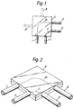
- FIGUREs 1 and 2 show a first example of the device according to the invention;
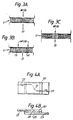
- FIGUREs 3A, 3B and 3C are diagrams showing alternative possibilities for the liquid crystal material used in the example of Figure 1 to form a waveguide linking two other waveguides;
- FIGUREs 4A and 4B are diagrams of the plan and sideviews of an alternative to the device shown in Figure 1 in which a waveguide written in liquid crystal material is used to link input and output waveguides embedded in the bounding planes;
- FIGURE 5 is a diagram of a ring resonator which could be formed in accordance with the present invention;
- FIGURE 6 is a diagram illustrating one way in which a diffraction grating according to the present invention could be produced;
- FIGURE 7 shows an alternative construction for a diffraction grating; and
- FIGUREs 8 and 9 show the use of regions of different refractive index produced in accordance with the present invention for refracting light propagating in a liquid crystal cell.
- Referring now to Figures 1 and 2, four
light waveguides 1, 2, 3 and 4 are joined to places on the periphery of a liquid crystal cell 5 of smectic A phase material. In the cell 5 there is drawn a waveguide 6 by one of the methods described above, for example by the use of a laser, the guide 6 joining the places where thewaveguides 1 and 4 meet the periphery of the cell 5. Light propagated along theguide 1 will be conveyed by the guide 6 to the guide 4. A second waveguide 7 is shown in Figure 1 joining the waveguides 2 and 3. If it were required to join thewaveguide 1 to the waveguide 3, then the cell 5 would be heated or subjected to a strong electric field to erase the guides 6 and 7 after which a new guide could be drawn joining thewaveguide 1 to the waveguide 3 by means of a laser, for example.Other waveguides 8 and 9 shown in Figure 1 could abut the periphery of the cell 5 and could be selectively connected to the other waveguides abutting the cell by guides drawn in the material of the cell itself. Since the refractive index of the liquid crystal material depends on the direction of the polarisation of the light, suitably aligned polarisers may be located where the external waveguides abut the periphery of the cell. Suitable matching interfaces should also be provided where thelight waveguides 1, 2, 3 and 4 are joined to the cell 5 to reduce the attenuation of the light transmitted due to changes in the refractive index of the material through which the light is propagating. - The interfaces may include lenses or other imaging optics at the ends of the waveguides as well as anti-reflection coatings.
- The waveguides in the cell 5 may be drawn in three ways which are shown in diagrammatic form in Figures 3A, 3B and 3C. In Figure 3A, the guiding region 10 of the liquid crystal material 11 is formed by changing the state in the region 10, of the originally homogeneously aligned material, poled to be homeotropically aligned, to be again homogeneously aligned in the region 10 by writing with a laser deflected along the path required for the waveguide. The light would of course be so polarised that the refractive index presented to the light of the guiding region 10 is higher than that of the remainder of the material which bounds it. Figure 3B shows a method of forming a guiding
region 12 of homeotropically aligned material bounded by borderingregions 13 and 14 in which it is the borderingregions 13 and 14 which are of homogeneously aligned material whilst the remainder of the liquid crystal material 11 is homeotropically aligned. The tworegions 13, 14 one on each side of the guidingregion 12 are written by deflecting the laser along the two substantially parallel paths so that theunmodified guiding region 12 between them can act as a light waveguide. - In Figures 3A and 3B, the liquid crystal material is initially homogeneously aligned and the whole of it is then poled by the application of a transverse electric field to be homeotropically aligned, As indicated in the Figures, this leaves a boundary layer of molecules adjacent the major bounding planes which remain in homogeneous alignment. This has the result that the cell of liquid crystal material is effectively homeotropically aligned and selected regions of it are restored to homogeneous alignment.
- In Figure 3C, the starting state of the liquid crystal material is again homogeneous whilst the guiding region is homeotropic. However, in this case, the
homeotropic guiding region 15 is formed by the selective application of local heating whilst a weak transverse electric field is applied generally or selectively to the materials. Alternatively, a guiding region of homogeneously aligned material could have been made by writing two closely spaced lines of homeotropic material in the cell similar to the arrangement illustrated in Figure 3B. - The deflection of the light spot from the laser may be achieved by the use of one or more mirrors rotated by an electro-mechanical arrangement having one or more moving coils mounted for rotation in a magnetic field. Alternatively commercially available acousto-optic beam deflectors may be used.
- The device shown in Figures 4A and 4B is similar to that shown in Figures 1 and 2 except that in this case a written guide 21 in a
liquid crystal cell 20 is used to join aninput guide 22 to anoutput guide 23 which meet thecell 20 on itsmajor faces waveguides - The guides drawn in the liquid crystal cell are not limited to being simply switchable from one position to another, but could be constructed in the form of evanescent field couplers, ring resonators or other passive optical components. In Figure 5, four
external waveguides cell 35, and guidingregions 36 and 37 are written in the material of thecell 35 by one of the methods described above and aclosed guiding ring 38 is written coupling together theregions 36 and 37. - Another possibility for the regions of different refractive index in the material of the cell is to cause a plurality of parallel lines to be dawn in the materiial of the cell so that it acts as a diffraction grating for light entering the cell through one of its major faces and leaving it through the other. Figure 6 is a diagram of such an arrangement in which a
cell 40 having major faces 41 and 42 has lines written in it parallel to each other going in and out of the plane of the paper by awrite beam 43 which is deflected backwards and forwards across the cell by ascanning mirror 44. The write beam is reflected onto the cell by a partiallytransmissive mirror 45 through which mirror asignal light beam 46 can pass to thecell 40. An output light beam 4 leaves thecell 40 at an angle to thesignal beam 46 due to the diffraction effect of the lines drawn in thecell 40. - The diffraction grating effect could also be used in the plane of the cell by writing a line of suitably spaced dots across the cell. This is shown diagramatically in Figure 7 in which a
cell 50 is provided with aline 51 of dots across the centre and light from aninput guide 52 meeting the cell at one place on its periphery is deflected to anoutput guide 53 at a place on the opposite side of the cell. This device could be used as an optical switch by changing the size and spacing of the dots so that the light could alternatively be deflected to anotheroutput waveguide 54. Means should be provided to ensure that the light propagating within the cell can pass to the output waveguides without being reflected back into the cell. - If larger regions than the narrow lines and dots referred to above are changed in state in the liquid crystal cell, then use may be made of the refraction of light propagating in the cell. Figure 8 shows a
cell 60 having aband 61 of higher refractive index formed in it which is used to deflect light from aninput waveguide 62 to anoutput waveguide 63. In Figure 9, acell 70 has a convex lens shapedregion 71 of higher refractive index formed in it and a second concave lens shapedregion 72 formed at one edge. Light frominput waveguides region 71 to theregion 72 where the light leaves by anoutput waveguide 75. - Although the invention has been described with reference to planar liquid crystal cells, they need not be planar but may be curved in one or two planes, the change in refractive index between the liquid crystal material and the glass or other material of the bounding surfaces being arranged to effect the light guiding required to keep the light in the liquid crystal material if necessary. Moreover the cell need not be of uniform thickness.
- Although the invention has been described with reference to specific examples, many other examples will be apparent to those skilled in the art.
Claims (17)
- A liquid crystal device (5) for guiding optical waves comprising:
a layer of liquid crystal material (11) interposed between two major bounding surfaces;
said liquid crystal material having an anisotropy in refractive indices and
said layer of liquid crystal material having at least one first region wherein the liquid crystal molecules are in a first state of molecular orientation and having second regions wherein the liquid crystal molecules are in a second state of molecular orientation, the molecular orientation in one of said states being substantially homogenous and the molecular orientation in the other of said states being substantially homeotropic
characterised in that said liquid crystal material (11) is in the smectic A phase. - A liquid crystal device according to claim 1 further comprising optical signal input means (1, 2) disposed to launch polarised optical signals into said first region, and optical signal output means (3, 4) disposed to collect polarised optical signals from said first region.
- A liquid crystal device according to claim 2 wherein the input means includes at least one first optical fibre (1, 2, 22, 31, 32, 52, 62, 73, 74) and the output means includes at least one second optical fibre (3, 4, 23, 33, 34, 54, 63, 75), the refractive index of the material in the second regions being lower than the refractive index of the material in the first region whereby at least one optical waveguide path is formed in the liquid crystal material between at least one first optical fibre and at least one second optical fibre.
- A liquid crystal device according to claim 3 wherein each waveguide path extends in a direction substantially parallel to the major bounding surfaces.
- A liquid crystal device according to claim 2 or claim 3 wherein the optical signals pass through said first region without intersecting the major bounding surfaces.
- A liquid crystal device according to claim 3 wherein at least one of the optical fibres overlies at least said first region.
- A liquid crystal device according to claim 3, wherein at least one of the optical fibres is disposed adjacent to, and parallel with, said first region.
- A liquid crystal device according to any one of claims 2 to 7, wherein at least one of said first and second regions defines a structure for refracting an input polarised optical signal as it passes through.
- A liquid crystal device according to claim 8, wherein said structure includes a diffraction grating formed by periodic interruptions in at least one of said first and second regions.
- A liquid crystal device according to claim 3 or claim 4, further comprising means for selectively reconfiguring said first and second regions so as to selectively change the direction of the waveguide path through the device.
- A liquid crystal device according to claim 10 in which the reconfiguring means includes means for selectively altering the molecular orientation of at least some of the liquid crystal material.
- A liquid crystal device according to claim 11, wherein the means for selectively altering the molecular orientation comprises means for locally heating the liquid crystal material out of the smectic A phase and means for applying an electric field to the material.
- A liquid crystal device according to claim 12, wherein the means for locally heating comprises a laser.
- A liquid crystal device according to claim 2, wherein the input means direct light into the liquid crystal material in a direction substantially perpendicular to the major bounding surfaces.
- A liquid crystal device according to any one of the claims 2 to 5 in which the input means direct light into the liquid crystal material in a direction substantially parallel to the major bounding surfaces.
- A method of reconfiguring a liquid crystal device for guiding optical waves according to claim 1 characterized by
poling the molecules of the liquid crystal material into a homeotropic alignment by applying an electric field substantially perpendicular to the major bounding surfaces;
removing the electric field; and
selectively heating a portion of the homeotropically aligned material out of the smectic A phase and allowing that portion to cool back into the smectic A phase to assume homogenous alignment, the portion being selected according to the desired function of the reconfigured component. - A method according to claim 16, comprising the step of selectively heating a portion of the liquid crystal material by using a laser.
Priority Applications (1)
| Application Number | Priority Date | Filing Date | Title |
|---|---|---|---|
| AT87302816T ATE99428T1 (en) | 1986-04-04 | 1987-03-31 | LIQUID CRYSTAL OPTICAL DEVICES. |
Applications Claiming Priority (2)
| Application Number | Priority Date | Filing Date | Title |
|---|---|---|---|
| GB8608276 | 1986-04-04 | ||
| GB868608276A GB8608276D0 (en) | 1986-04-04 | 1986-04-04 | Optical devices |
Publications (2)
| Publication Number | Publication Date |
|---|---|
| EP0249311A1 EP0249311A1 (en) | 1987-12-16 |
| EP0249311B1 true EP0249311B1 (en) | 1993-12-29 |
Family
ID=10595697
Family Applications (1)
| Application Number | Title | Priority Date | Filing Date |
|---|---|---|---|
| EP87302816A Expired - Lifetime EP0249311B1 (en) | 1986-04-04 | 1987-03-31 | Liquid crystal optical devices |
Country Status (8)
| Country | Link |
|---|---|
| US (1) | US4893907A (en) |
| EP (1) | EP0249311B1 (en) |
| JP (1) | JPS63503095A (en) |
| AT (1) | ATE99428T1 (en) |
| CA (1) | CA1304489C (en) |
| DE (1) | DE3788595T2 (en) |
| GB (1) | GB8608276D0 (en) |
| WO (1) | WO1987006019A1 (en) |
Families Citing this family (20)
| Publication number | Priority date | Publication date | Assignee | Title |
|---|---|---|---|---|
| US4974941A (en) * | 1989-03-08 | 1990-12-04 | Hercules Incorporated | Process of aligning and realigning liquid crystal media |
| WO1990014611A1 (en) * | 1989-05-25 | 1990-11-29 | Optical Shields, Inc. | High speed optical protection using smectic liquid crystal |
| US5159475A (en) * | 1989-05-25 | 1992-10-27 | Optical Shields, Inc. | High speed optical protection using smectic liquid crystal |
| US5073294A (en) * | 1990-03-07 | 1991-12-17 | Hercules Incorporated | Process of preparing compositions having multiple oriented mesogens |
| EP0525473B1 (en) * | 1991-07-26 | 1998-05-06 | Rolic AG | Liquid crystal cell |
| EP0525478B1 (en) * | 1991-07-26 | 1997-06-11 | F. Hoffmann-La Roche Ag | Liquid crystal display cell |
| DE59205351D1 (en) * | 1991-12-05 | 1996-03-28 | Hoffmann La Roche | Micromechanical process for structuring a polymer alignment layer |
| US5381251A (en) * | 1992-04-07 | 1995-01-10 | Sharp Kabushiki Kaisha | Optical switch element and a liquid crystal light directional coupler used in the optical switch element |
| US5928819A (en) * | 1996-12-19 | 1999-07-27 | Xerox Corporation | Methods to fabricate optical equivalents of fiber optic face plates using reactive liquid crystals and polymers |
| US5726730A (en) * | 1996-12-19 | 1998-03-10 | Xerox Corporation | Optical equivalents of fiber optic face plates using reactive liquid crystals and polymers |
| US6160606A (en) * | 1997-08-05 | 2000-12-12 | Xerox Corporation | Optical equivalents of fiber optic face plates using irradiation sensitive glass |
| GB2341454B (en) * | 1998-09-14 | 2003-01-29 | Univ Southampton | Optical waveguide and method of fabricating the same |
| EP1139150A1 (en) * | 2000-03-27 | 2001-10-04 | Hewlett-Packard Company, A Delaware Corporation | Liquid crystal alignment structure |
| EP1139151B1 (en) * | 2000-03-27 | 2007-05-16 | Hewlett-Packard Company, A Delaware Corporation | Bistable nematic liquid crystal device |
| US7460200B2 (en) * | 2000-03-27 | 2008-12-02 | Helwett-Packard Development Company, L.P. | Liquid crystal alignment |
| EP1139152A1 (en) * | 2000-03-27 | 2001-10-04 | Hewlett-Packard Company, A Delaware Corporation | Liquid crystal alignment structure |
| EP1271225A1 (en) * | 2001-06-22 | 2003-01-02 | Hewlett-Packard Company, A Delaware Corporation | Bistable nematic liquid crystal device |
| US6999649B1 (en) * | 2001-10-26 | 2006-02-14 | Kent Optronics Inc. | Optical switches made by nematic liquid crystal switchable mirrors, and apparatus of manufacture |
| US6785439B2 (en) * | 2002-01-29 | 2004-08-31 | Agilent Technologies, Inc. | Switching using three-dimensional rewriteable waveguide in photosensitive media |
| CN110658585B (en) * | 2018-06-29 | 2022-01-11 | 华为技术有限公司 | Optical waveguide device |
Family Cites Families (18)
| Publication number | Priority date | Publication date | Assignee | Title |
|---|---|---|---|---|
| US3796999A (en) * | 1972-10-19 | 1974-03-12 | Bell Telephone Labor Inc | Locally erasable thermo-optic smectic liquid crystal storage displays |
| US3963310A (en) * | 1973-08-20 | 1976-06-15 | The United States Of America As Represented By The Secretary Of The Navy | Liquid crystal waveguide |
| JPS54185B2 (en) * | 1974-02-28 | 1979-01-08 | ||
| FR2296197A1 (en) * | 1974-12-24 | 1976-07-23 | Thomson Csf | METHOD AND DEVICE USING A THERMO-OPTICAL EFFECT IN A THIN LAYER IN SMECTIC PHASE FOR THE REPRODUCTION OF IMAGES WITH MEMORY |
| FR2373076A1 (en) * | 1976-12-03 | 1978-06-30 | Thomson Csf | LIQUID CRYSTAL CELL |
| JPS54103063A (en) * | 1978-01-30 | 1979-08-14 | Nec Corp | Projection type crystal display device and driving method thereof |
| JPS5522772A (en) * | 1978-08-08 | 1980-02-18 | Nec Corp | Liquid crystal display device |
| US4201442A (en) * | 1978-10-02 | 1980-05-06 | Sperry Corporation | Liquid crystal switching coupler matrix |
| US4563059A (en) * | 1983-01-10 | 1986-01-07 | Clark Noel A | Surface stabilized ferroelectric liquid crystal devices |
| JPS5887535A (en) * | 1981-11-20 | 1983-05-25 | Sony Corp | Liquid crystal display |
| JPS58123506A (en) * | 1982-01-19 | 1983-07-22 | Ritsuo Hasumi | Thick film optical integrated circuit of diffusion type |
| JPH0629919B2 (en) * | 1982-04-16 | 1994-04-20 | 株式会社日立製作所 | Liquid crystal element driving method |
| JPS5969732U (en) * | 1982-11-02 | 1984-05-11 | 旭硝子株式会社 | sauna equipment |
| JPS59143131U (en) * | 1983-03-15 | 1984-09-25 | 三菱重工業株式会社 | Waterproof cover for precision electronic equipment |
| JPS6083009A (en) * | 1983-10-13 | 1985-05-11 | Mitsubishi Electric Corp | Photoswitch |
| JPS60107023A (en) * | 1983-11-15 | 1985-06-12 | Canon Inc | liquid crystal device |
| GB2161951B (en) * | 1984-07-17 | 1988-01-20 | Stc Plc | Laser addressed smectic displays |
| JPS61118725A (en) * | 1984-11-14 | 1986-06-06 | Sharp Corp | Optical memory readout system by laser oscillation of rewritable medium using smectic guest-host type liquid crystal |
-
1986
- 1986-04-04 GB GB868608276A patent/GB8608276D0/en active Pending
-
1987
- 1987-03-31 WO PCT/GB1987/000217 patent/WO1987006019A1/en not_active Ceased
- 1987-03-31 EP EP87302816A patent/EP0249311B1/en not_active Expired - Lifetime
- 1987-03-31 US US07/130,462 patent/US4893907A/en not_active Expired - Fee Related
- 1987-03-31 AT AT87302816T patent/ATE99428T1/en not_active IP Right Cessation
- 1987-03-31 DE DE87302816T patent/DE3788595T2/en not_active Expired - Fee Related
- 1987-03-31 JP JP62502161A patent/JPS63503095A/en active Pending
- 1987-04-03 CA CA000533829A patent/CA1304489C/en not_active Expired - Lifetime
Also Published As
| Publication number | Publication date |
|---|---|
| DE3788595T2 (en) | 1994-04-28 |
| DE3788595D1 (en) | 1994-02-10 |
| ATE99428T1 (en) | 1994-01-15 |
| CA1304489C (en) | 1992-06-30 |
| US4893907A (en) | 1990-01-16 |
| GB8608276D0 (en) | 1986-05-08 |
| EP0249311A1 (en) | 1987-12-16 |
| JPS63503095A (en) | 1988-11-10 |
| WO1987006019A1 (en) | 1987-10-08 |
Similar Documents
| Publication | Publication Date | Title |
|---|---|---|
| US4893907A (en) | Optical devices | |
| US3963310A (en) | Liquid crystal waveguide | |
| US5481636A (en) | Wavelength conversion element | |
| US4201442A (en) | Liquid crystal switching coupler matrix | |
| Karpierz et al. | Self focusing in liquid crystalline waveguides | |
| US6111633A (en) | Polarization independent optical switching device | |
| US7215842B2 (en) | Light control element and light control device | |
| US4983006A (en) | Polarization-independent optical waveguide switch | |
| US3967877A (en) | Coupler for coupling optical energy transmitted by optical fiber to optical waveguide and method of manufacture | |
| US4836657A (en) | Optical change-over switch utilizing ferroelectric liquid crystal material | |
| US4094579A (en) | Multimode optical waveguide device with non-normal butt coupling of fiber to electro-optic planar waveguide | |
| EP0624812B1 (en) | Liquid crystal light modulation device | |
| Rushnova et al. | Integrated-optical nematic liquid crystal switches: designing and operation features | |
| Gros et al. | Ferroelectric liquid crystal optical waveguide switches using the double-refraction effect | |
| US5835644A (en) | TE-pass optical waveguide polarizer using elecro-optic polymers | |
| US3993400A (en) | Method and apparatus for forming erasable, real time, optical circuits | |
| Xu et al. | Polymer planar waveguide device using inverted channel structure with upper liquid crystal cladding | |
| Chang | Guided-wave two-dimensional acousto-optic scanner using proton-exchanged lithium niobate waveguide | |
| d'Alessandro et al. | Integrated optic devices using liquid crystals: design and fabrication issues | |
| Sirleto et al. | Fast integrated electro-optical switch and beam deflector based on nematic liquid crystal waveguides | |
| JPH05249506A (en) | Optical switch | |
| Pishnyak et al. | Liquid crystal digital beam steering device based on decoupled birefringent deflector and polarization rotator | |
| JPH0371114A (en) | Optical switch | |
| US5159475A (en) | High speed optical protection using smectic liquid crystal | |
| JP3031394B2 (en) | Transmission wavelength control method |
Legal Events
| Date | Code | Title | Description |
|---|---|---|---|
| PUAI | Public reference made under article 153(3) epc to a published international application that has entered the european phase |
Free format text: ORIGINAL CODE: 0009012 |
|
| AK | Designated contracting states |
Kind code of ref document: A1 Designated state(s): AT BE CH DE ES FR GB GR IT LI LU NL SE |
|
| 17P | Request for examination filed |
Effective date: 19880520 |
|
| 17Q | First examination report despatched |
Effective date: 19910718 |
|
| GRAA | (expected) grant |
Free format text: ORIGINAL CODE: 0009210 |
|
| AK | Designated contracting states |
Kind code of ref document: B1 Designated state(s): AT BE CH DE ES FR GB GR IT LI LU NL SE |
|
| PG25 | Lapsed in a contracting state [announced via postgrant information from national office to epo] |
Ref country code: LI Effective date: 19931229 Ref country code: GR Free format text: LAPSE BECAUSE OF FAILURE TO SUBMIT A TRANSLATION OF THE DESCRIPTION OR TO PAY THE FEE WITHIN THE PRESCRIBED TIME-LIMIT Effective date: 19931229 Ref country code: CH Effective date: 19931229 Ref country code: BE Effective date: 19931229 Ref country code: AT Effective date: 19931229 |
|
| REF | Corresponds to: |
Ref document number: 99428 Country of ref document: AT Date of ref document: 19940115 Kind code of ref document: T |
|
| ITF | It: translation for a ep patent filed | ||
| REF | Corresponds to: |
Ref document number: 3788595 Country of ref document: DE Date of ref document: 19940210 |
|
| PG25 | Lapsed in a contracting state [announced via postgrant information from national office to epo] |
Ref country code: LU Free format text: LAPSE BECAUSE OF NON-PAYMENT OF DUE FEES Effective date: 19940331 |
|
| PG25 | Lapsed in a contracting state [announced via postgrant information from national office to epo] |
Ref country code: ES Free format text: LAPSE BECAUSE OF FAILURE TO SUBMIT A TRANSLATION OF THE DESCRIPTION OR TO PAY THE FEE WITHIN THE PRESCRIBED TIME-LIMIT Effective date: 19940409 |
|
| REG | Reference to a national code |
Ref country code: CH Ref legal event code: PL |
|
| ET | Fr: translation filed | ||
| PLBE | No opposition filed within time limit |
Free format text: ORIGINAL CODE: 0009261 |
|
| STAA | Information on the status of an ep patent application or granted ep patent |
Free format text: STATUS: NO OPPOSITION FILED WITHIN TIME LIMIT |
|
| 26N | No opposition filed | ||
| EAL | Se: european patent in force in sweden |
Ref document number: 87302816.1 |
|
| PGFP | Annual fee paid to national office [announced via postgrant information from national office to epo] |
Ref country code: SE Payment date: 19950213 Year of fee payment: 9 |
|
| PGFP | Annual fee paid to national office [announced via postgrant information from national office to epo] |
Ref country code: NL Payment date: 19950331 Year of fee payment: 9 |
|
| PGFP | Annual fee paid to national office [announced via postgrant information from national office to epo] |
Ref country code: FR Payment date: 19960208 Year of fee payment: 10 |
|
| PGFP | Annual fee paid to national office [announced via postgrant information from national office to epo] |
Ref country code: DE Payment date: 19960227 Year of fee payment: 10 |
|
| PG25 | Lapsed in a contracting state [announced via postgrant information from national office to epo] |
Ref country code: SE Effective date: 19960401 |
|
| PG25 | Lapsed in a contracting state [announced via postgrant information from national office to epo] |
Ref country code: NL Effective date: 19961001 |
|
| NLV4 | Nl: lapsed or anulled due to non-payment of the annual fee |
Effective date: 19961001 |
|
| EUG | Se: european patent has lapsed |
Ref document number: 87302816.1 |
|
| PG25 | Lapsed in a contracting state [announced via postgrant information from national office to epo] |
Ref country code: FR Free format text: LAPSE BECAUSE OF NON-PAYMENT OF DUE FEES Effective date: 19971128 |
|
| PG25 | Lapsed in a contracting state [announced via postgrant information from national office to epo] |
Ref country code: DE Effective date: 19971202 |
|
| REG | Reference to a national code |
Ref country code: FR Ref legal event code: ST |
|
| REG | Reference to a national code |
Ref country code: GB Ref legal event code: 732E |
|
| REG | Reference to a national code |
Ref country code: GB Ref legal event code: IF02 |
|
| PGFP | Annual fee paid to national office [announced via postgrant information from national office to epo] |
Ref country code: GB Payment date: 20020220 Year of fee payment: 16 |
|
| PG25 | Lapsed in a contracting state [announced via postgrant information from national office to epo] |
Ref country code: GB Free format text: LAPSE BECAUSE OF NON-PAYMENT OF DUE FEES Effective date: 20030331 |
|
| GBPC | Gb: european patent ceased through non-payment of renewal fee |
Effective date: 20030331 |
|
| PG25 | Lapsed in a contracting state [announced via postgrant information from national office to epo] |
Ref country code: IT Free format text: LAPSE BECAUSE OF NON-PAYMENT OF DUE FEES Effective date: 20050331 |