EP0246808B1 - Solid electrolytic capacitor - Google Patents
Solid electrolytic capacitor Download PDFInfo
- Publication number
- EP0246808B1 EP0246808B1 EP87304261A EP87304261A EP0246808B1 EP 0246808 B1 EP0246808 B1 EP 0246808B1 EP 87304261 A EP87304261 A EP 87304261A EP 87304261 A EP87304261 A EP 87304261A EP 0246808 B1 EP0246808 B1 EP 0246808B1
- Authority
- EP
- European Patent Office
- Prior art keywords
- valve metal
- lead
- foils
- electrolytic capacitor
- solid electrolytic
- Prior art date
- Legal status (The legal status is an assumption and is not a legal conclusion. Google has not performed a legal analysis and makes no representation as to the accuracy of the status listed.)
- Expired - Lifetime
Links
- 239000003990 capacitor Substances 0.000 title claims description 120
- 239000007787 solid Substances 0.000 title claims description 88
- 239000011888 foil Substances 0.000 claims description 228
- 239000010410 layer Substances 0.000 claims description 138
- 229910052751 metal Inorganic materials 0.000 claims description 97
- 239000002184 metal Substances 0.000 claims description 97
- YADSGOSSYOOKMP-UHFFFAOYSA-N dioxolead Chemical compound O=[Pb]=O YADSGOSSYOOKMP-UHFFFAOYSA-N 0.000 claims description 88
- 239000004065 semiconductor Substances 0.000 claims description 79
- 150000001875 compounds Chemical class 0.000 claims description 33
- 238000000034 method Methods 0.000 claims description 32
- 239000007788 liquid Substances 0.000 claims description 28
- RVPVRDXYQKGNMQ-UHFFFAOYSA-N lead(2+) Chemical compound [Pb+2] RVPVRDXYQKGNMQ-UHFFFAOYSA-N 0.000 claims description 24
- PIJPYDMVFNTHIP-UHFFFAOYSA-L lead sulfate Chemical compound [PbH4+2].[O-]S([O-])(=O)=O PIJPYDMVFNTHIP-UHFFFAOYSA-L 0.000 claims description 20
- 125000006850 spacer group Chemical group 0.000 claims description 20
- 239000002344 surface layer Substances 0.000 claims description 15
- 238000006243 chemical reaction Methods 0.000 claims description 12
- 239000007800 oxidant agent Substances 0.000 claims description 12
- 230000001590 oxidative effect Effects 0.000 claims description 11
- 239000000463 material Substances 0.000 claims description 10
- JRKICGRDRMAZLK-UHFFFAOYSA-L peroxydisulfate Chemical compound [O-]S(=O)(=O)OOS([O-])(=O)=O JRKICGRDRMAZLK-UHFFFAOYSA-L 0.000 claims description 9
- 238000005234 chemical deposition Methods 0.000 claims description 5
- 238000004070 electrodeposition Methods 0.000 claims description 3
- 238000004519 manufacturing process Methods 0.000 claims description 3
- XAGFODPZIPBFFR-UHFFFAOYSA-N aluminium Chemical compound [Al] XAGFODPZIPBFFR-UHFFFAOYSA-N 0.000 description 33
- 229910052782 aluminium Inorganic materials 0.000 description 30
- 239000007864 aqueous solution Substances 0.000 description 21
- 239000000758 substrate Substances 0.000 description 16
- 238000010586 diagram Methods 0.000 description 15
- MHAJPDPJQMAIIY-UHFFFAOYSA-N Hydrogen peroxide Chemical compound OO MHAJPDPJQMAIIY-UHFFFAOYSA-N 0.000 description 14
- 239000000203 mixture Substances 0.000 description 14
- ROOXNKNUYICQNP-UHFFFAOYSA-N ammonium persulfate Chemical compound [NH4+].[NH4+].[O-]S(=O)(=O)OOS([O-])(=O)=O ROOXNKNUYICQNP-UHFFFAOYSA-N 0.000 description 10
- 229940046892 lead acetate Drugs 0.000 description 10
- 230000003647 oxidation Effects 0.000 description 8
- 238000007254 oxidation reaction Methods 0.000 description 8
- 239000000243 solution Substances 0.000 description 8
- 238000004458 analytical method Methods 0.000 description 6
- 239000003792 electrolyte Substances 0.000 description 6
- TWNQGVIAIRXVLR-UHFFFAOYSA-N oxo(oxoalumanyloxy)alumane Chemical compound O=[Al]O[Al]=O TWNQGVIAIRXVLR-UHFFFAOYSA-N 0.000 description 6
- 239000011347 resin Substances 0.000 description 6
- 229920005989 resin Polymers 0.000 description 6
- XLYOFNOQVPJJNP-UHFFFAOYSA-N water Substances O XLYOFNOQVPJJNP-UHFFFAOYSA-N 0.000 description 6
- 229910001870 ammonium persulfate Inorganic materials 0.000 description 5
- 230000015572 biosynthetic process Effects 0.000 description 5
- 230000000052 comparative effect Effects 0.000 description 5
- 239000003960 organic solvent Substances 0.000 description 5
- 238000007747 plating Methods 0.000 description 5
- PXHVJJICTQNCMI-UHFFFAOYSA-N Nickel Chemical compound [Ni] PXHVJJICTQNCMI-UHFFFAOYSA-N 0.000 description 4
- KGBXLFKZBHKPEV-UHFFFAOYSA-N boric acid Chemical compound OB(O)O KGBXLFKZBHKPEV-UHFFFAOYSA-N 0.000 description 4
- 239000004327 boric acid Substances 0.000 description 4
- NUJOXMJBOLGQSY-UHFFFAOYSA-N manganese dioxide Chemical compound O=[Mn]=O NUJOXMJBOLGQSY-UHFFFAOYSA-N 0.000 description 4
- 238000002360 preparation method Methods 0.000 description 4
- 239000000126 substance Substances 0.000 description 4
- WYXIGTJNYDDFFH-UHFFFAOYSA-Q triazanium;borate Chemical compound [NH4+].[NH4+].[NH4+].[O-]B([O-])[O-] WYXIGTJNYDDFFH-UHFFFAOYSA-Q 0.000 description 4
- UHOVQNZJYSORNB-UHFFFAOYSA-N Benzene Chemical compound C1=CC=CC=C1 UHOVQNZJYSORNB-UHFFFAOYSA-N 0.000 description 3
- OKTJSMMVPCPJKN-UHFFFAOYSA-N Carbon Chemical compound [C] OKTJSMMVPCPJKN-UHFFFAOYSA-N 0.000 description 3
- RYGMFSIKBFXOCR-UHFFFAOYSA-N Copper Chemical compound [Cu] RYGMFSIKBFXOCR-UHFFFAOYSA-N 0.000 description 3
- PEDCQBHIVMGVHV-UHFFFAOYSA-N Glycerine Chemical compound OCC(O)CO PEDCQBHIVMGVHV-UHFFFAOYSA-N 0.000 description 3
- BQCADISMDOOEFD-UHFFFAOYSA-N Silver Chemical compound [Ag] BQCADISMDOOEFD-UHFFFAOYSA-N 0.000 description 3
- 238000002441 X-ray diffraction Methods 0.000 description 3
- KQNKJJBFUFKYFX-UHFFFAOYSA-N acetic acid;trihydrate Chemical compound O.O.O.CC(O)=O KQNKJJBFUFKYFX-UHFFFAOYSA-N 0.000 description 3
- 229910052799 carbon Inorganic materials 0.000 description 3
- 229910052802 copper Inorganic materials 0.000 description 3
- 239000010949 copper Substances 0.000 description 3
- 238000002329 infrared spectrum Methods 0.000 description 3
- RLJMLMKIBZAXJO-UHFFFAOYSA-N lead nitrate Chemical compound [O-][N+](=O)O[Pb]O[N+]([O-])=O RLJMLMKIBZAXJO-UHFFFAOYSA-N 0.000 description 3
- -1 porphyrin compound Chemical class 0.000 description 3
- 229910052709 silver Inorganic materials 0.000 description 3
- 239000004332 silver Substances 0.000 description 3
- 239000007784 solid electrolyte Substances 0.000 description 3
- 239000002904 solvent Substances 0.000 description 3
- 229910052715 tantalum Inorganic materials 0.000 description 3
- GUVRBAGPIYLISA-UHFFFAOYSA-N tantalum atom Chemical compound [Ta] GUVRBAGPIYLISA-UHFFFAOYSA-N 0.000 description 3
- 238000005979 thermal decomposition reaction Methods 0.000 description 3
- AZQWKYJCGOJGHM-UHFFFAOYSA-N 1,4-benzoquinone Chemical compound O=C1C=CC(=O)C=C1 AZQWKYJCGOJGHM-UHFFFAOYSA-N 0.000 description 2
- WHQOKFZWSDOTQP-UHFFFAOYSA-N 2,3-dihydroxypropyl 4-aminobenzoate Chemical compound NC1=CC=C(C(=O)OCC(O)CO)C=C1 WHQOKFZWSDOTQP-UHFFFAOYSA-N 0.000 description 2
- VEYIMQVTPXPUHA-UHFFFAOYSA-N 3-hydroxypyran-4-one Chemical compound OC1=COC=CC1=O VEYIMQVTPXPUHA-UHFFFAOYSA-N 0.000 description 2
- ZKQDCIXGCQPQNV-UHFFFAOYSA-N Calcium hypochlorite Chemical compound [Ca+2].Cl[O-].Cl[O-] ZKQDCIXGCQPQNV-UHFFFAOYSA-N 0.000 description 2
- HEDRZPFGACZZDS-UHFFFAOYSA-N Chloroform Chemical compound ClC(Cl)Cl HEDRZPFGACZZDS-UHFFFAOYSA-N 0.000 description 2
- IAZDPXIOMUYVGZ-UHFFFAOYSA-N Dimethylsulphoxide Chemical compound CS(C)=O IAZDPXIOMUYVGZ-UHFFFAOYSA-N 0.000 description 2
- LFQSCWFLJHTTHZ-UHFFFAOYSA-N Ethanol Chemical compound CCO LFQSCWFLJHTTHZ-UHFFFAOYSA-N 0.000 description 2
- 239000004743 Polypropylene Substances 0.000 description 2
- RTAQQCXQSZGOHL-UHFFFAOYSA-N Titanium Chemical compound [Ti] RTAQQCXQSZGOHL-UHFFFAOYSA-N 0.000 description 2
- YRKCREAYFQTBPV-UHFFFAOYSA-N acetylacetone Chemical compound CC(=O)CC(C)=O YRKCREAYFQTBPV-UHFFFAOYSA-N 0.000 description 2
- RGCKGOZRHPZPFP-UHFFFAOYSA-N alizarin Chemical compound C1=CC=C2C(=O)C3=C(O)C(O)=CC=C3C(=O)C2=C1 RGCKGOZRHPZPFP-UHFFFAOYSA-N 0.000 description 2
- HOQPTLCRWVZIQZ-UHFFFAOYSA-H bis[[2-(5-hydroxy-4,7-dioxo-1,3,2$l^{2}-dioxaplumbepan-5-yl)acetyl]oxy]lead Chemical compound [Pb+2].[Pb+2].[Pb+2].[O-]C(=O)CC(O)(CC([O-])=O)C([O-])=O.[O-]C(=O)CC(O)(CC([O-])=O)C([O-])=O HOQPTLCRWVZIQZ-UHFFFAOYSA-H 0.000 description 2
- YALMXYPQBUJUME-UHFFFAOYSA-L calcium chlorate Chemical compound [Ca+2].[O-]Cl(=O)=O.[O-]Cl(=O)=O YALMXYPQBUJUME-UHFFFAOYSA-L 0.000 description 2
- QXIKMJLSPJFYOI-UHFFFAOYSA-L calcium;dichlorite Chemical compound [Ca+2].[O-]Cl=O.[O-]Cl=O QXIKMJLSPJFYOI-UHFFFAOYSA-L 0.000 description 2
- ZASWJUOMEGBQCQ-UHFFFAOYSA-L dibromolead Chemical compound Br[Pb]Br ZASWJUOMEGBQCQ-UHFFFAOYSA-L 0.000 description 2
- XOYUVEPYBYHIFZ-UHFFFAOYSA-L diperchloryloxylead Chemical compound [Pb+2].[O-]Cl(=O)(=O)=O.[O-]Cl(=O)(=O)=O XOYUVEPYBYHIFZ-UHFFFAOYSA-L 0.000 description 2
- VLOJXAQYHIVPFI-UHFFFAOYSA-H lead(2+);diacetate;tetrahydroxide Chemical compound [OH-].[OH-].[OH-].[OH-].[Pb+2].[Pb+2].[Pb+2].CC([O-])=O.CC([O-])=O VLOJXAQYHIVPFI-UHFFFAOYSA-H 0.000 description 2
- RDQAROAGXMVOKC-UHFFFAOYSA-L lead(2+);dibromate Chemical compound [Pb+2].[O-]Br(=O)=O.[O-]Br(=O)=O RDQAROAGXMVOKC-UHFFFAOYSA-L 0.000 description 2
- NGXWSRYOFVTCCT-UHFFFAOYSA-L lead(2+);dichlorate Chemical compound [Pb+2].[O-]Cl(=O)=O.[O-]Cl(=O)=O NGXWSRYOFVTCCT-UHFFFAOYSA-L 0.000 description 2
- HWSZZLVAJGOAAY-UHFFFAOYSA-L lead(II) chloride Chemical compound Cl[Pb]Cl HWSZZLVAJGOAAY-UHFFFAOYSA-L 0.000 description 2
- 150000002739 metals Chemical class 0.000 description 2
- 229910052759 nickel Inorganic materials 0.000 description 2
- 229910052758 niobium Inorganic materials 0.000 description 2
- 239000010955 niobium Substances 0.000 description 2
- GUCVJGMIXFAOAE-UHFFFAOYSA-N niobium atom Chemical compound [Nb] GUCVJGMIXFAOAE-UHFFFAOYSA-N 0.000 description 2
- 229920001155 polypropylene Polymers 0.000 description 2
- 238000005476 soldering Methods 0.000 description 2
- 239000010936 titanium Substances 0.000 description 2
- 229910052719 titanium Inorganic materials 0.000 description 2
- RYHBNJHYFVUHQT-UHFFFAOYSA-N 1,4-Dioxane Chemical compound C1COCCO1 RYHBNJHYFVUHQT-UHFFFAOYSA-N 0.000 description 1
- LCPVQAHEFVXVKT-UHFFFAOYSA-N 2-(2,4-difluorophenoxy)pyridin-3-amine Chemical compound NC1=CC=CN=C1OC1=CC=C(F)C=C1F LCPVQAHEFVXVKT-UHFFFAOYSA-N 0.000 description 1
- BZSXEZOLBIJVQK-UHFFFAOYSA-N 2-methylsulfonylbenzoic acid Chemical compound CS(=O)(=O)C1=CC=CC=C1C(O)=O BZSXEZOLBIJVQK-UHFFFAOYSA-N 0.000 description 1
- 239000004342 Benzoyl peroxide Substances 0.000 description 1
- OMPJBNCRMGITSC-UHFFFAOYSA-N Benzoylperoxide Chemical compound C=1C=CC=CC=1C(=O)OOC(=O)C1=CC=CC=C1 OMPJBNCRMGITSC-UHFFFAOYSA-N 0.000 description 1
- 229910021578 Iron(III) chloride Inorganic materials 0.000 description 1
- 229920000297 Rayon Polymers 0.000 description 1
- XHCLAFWTIXFWPH-UHFFFAOYSA-N [O-2].[O-2].[O-2].[O-2].[O-2].[V+5].[V+5] Chemical compound [O-2].[O-2].[O-2].[O-2].[O-2].[V+5].[V+5] XHCLAFWTIXFWPH-UHFFFAOYSA-N 0.000 description 1
- PQLVXDKIJBQVDF-UHFFFAOYSA-N acetic acid;hydrate Chemical compound O.CC(O)=O PQLVXDKIJBQVDF-UHFFFAOYSA-N 0.000 description 1
- WRYNUJYAXVDTCB-UHFFFAOYSA-M acetyloxymercury Chemical compound CC(=O)O[Hg] WRYNUJYAXVDTCB-UHFFFAOYSA-M 0.000 description 1
- 229910045601 alloy Inorganic materials 0.000 description 1
- 239000000956 alloy Substances 0.000 description 1
- PNEYBMLMFCGWSK-UHFFFAOYSA-N aluminium oxide Inorganic materials [O-2].[O-2].[O-2].[Al+3].[Al+3] PNEYBMLMFCGWSK-UHFFFAOYSA-N 0.000 description 1
- 235000019400 benzoyl peroxide Nutrition 0.000 description 1
- KRVSOGSZCMJSLX-UHFFFAOYSA-L chromic acid Substances O[Cr](O)(=O)=O KRVSOGSZCMJSLX-UHFFFAOYSA-L 0.000 description 1
- 239000002633 crown compound Substances 0.000 description 1
- 238000000151 deposition Methods 0.000 description 1
- 230000008021 deposition Effects 0.000 description 1
- 239000003989 dielectric material Substances 0.000 description 1
- 238000007598 dipping method Methods 0.000 description 1
- 235000019441 ethanol Nutrition 0.000 description 1
- 238000002474 experimental method Methods 0.000 description 1
- AWJWCTOOIBYHON-UHFFFAOYSA-N furo[3,4-b]pyrazine-5,7-dione Chemical compound C1=CN=C2C(=O)OC(=O)C2=N1 AWJWCTOOIBYHON-UHFFFAOYSA-N 0.000 description 1
- 238000007654 immersion Methods 0.000 description 1
- 238000010348 incorporation Methods 0.000 description 1
- 239000011810 insulating material Substances 0.000 description 1
- 150000002500 ions Chemical class 0.000 description 1
- RBTARNINKXHZNM-UHFFFAOYSA-K iron trichloride Chemical compound Cl[Fe](Cl)Cl RBTARNINKXHZNM-UHFFFAOYSA-K 0.000 description 1
- 238000002955 isolation Methods 0.000 description 1
- 239000005001 laminate film Substances 0.000 description 1
- 229910052745 lead Inorganic materials 0.000 description 1
- ZGUQQOOKFJPJRS-UHFFFAOYSA-N lead silicon Chemical compound [Si].[Pb] ZGUQQOOKFJPJRS-UHFFFAOYSA-N 0.000 description 1
- WABPQHHGFIMREM-UHFFFAOYSA-N lead(0) Chemical group [Pb] WABPQHHGFIMREM-UHFFFAOYSA-N 0.000 description 1
- MIVBAHRSNUNMPP-UHFFFAOYSA-N manganese(2+);dinitrate Chemical compound [Mn+2].[O-][N+]([O-])=O.[O-][N+]([O-])=O MIVBAHRSNUNMPP-UHFFFAOYSA-N 0.000 description 1
- 230000004048 modification Effects 0.000 description 1
- 238000012986 modification Methods 0.000 description 1
- 229920002689 polyvinyl acetate Polymers 0.000 description 1
- 239000011118 polyvinyl acetate Substances 0.000 description 1
- 239000012286 potassium permanganate Substances 0.000 description 1
- USHAGKDGDHPEEY-UHFFFAOYSA-L potassium persulfate Chemical compound [K+].[K+].[O-]S(=O)(=O)OOS([O-])(=O)=O USHAGKDGDHPEEY-UHFFFAOYSA-L 0.000 description 1
- ILVXOBCQQYKLDS-UHFFFAOYSA-N pyridine N-oxide Chemical compound [O-][N+]1=CC=CC=C1 ILVXOBCQQYKLDS-UHFFFAOYSA-N 0.000 description 1
- MCJGNVYPOGVAJF-UHFFFAOYSA-N quinolin-8-ol Chemical compound C1=CN=C2C(O)=CC=CC2=C1 MCJGNVYPOGVAJF-UHFFFAOYSA-N 0.000 description 1
- 239000002964 rayon Substances 0.000 description 1
- YGSDEFSMJLZEOE-UHFFFAOYSA-N salicylic acid Chemical compound OC(=O)C1=CC=CC=C1O YGSDEFSMJLZEOE-UHFFFAOYSA-N 0.000 description 1
- JPJALAQPGMAKDF-UHFFFAOYSA-N selenium dioxide Chemical compound O=[Se]=O JPJALAQPGMAKDF-UHFFFAOYSA-N 0.000 description 1
- 229910052710 silicon Inorganic materials 0.000 description 1
- 239000010703 silicon Substances 0.000 description 1
- CHQMHPLRPQMAMX-UHFFFAOYSA-L sodium persulfate Substances [Na+].[Na+].[O-]S(=O)(=O)OOS([O-])(=O)=O CHQMHPLRPQMAMX-UHFFFAOYSA-L 0.000 description 1
- 229910000679 solder Inorganic materials 0.000 description 1
- 238000007711 solidification Methods 0.000 description 1
- 230000008023 solidification Effects 0.000 description 1
- IIACRCGMVDHOTQ-UHFFFAOYSA-M sulfamate Chemical compound NS([O-])(=O)=O IIACRCGMVDHOTQ-UHFFFAOYSA-M 0.000 description 1
- UGNWTBMOAKPKBL-UHFFFAOYSA-N tetrachloro-1,4-benzoquinone Chemical compound ClC1=C(Cl)C(=O)C(Cl)=C(Cl)C1=O UGNWTBMOAKPKBL-UHFFFAOYSA-N 0.000 description 1
- 238000001771 vacuum deposition Methods 0.000 description 1
- 229910001935 vanadium oxide Inorganic materials 0.000 description 1
Images





Classifications
-
- H—ELECTRICITY
- H01—ELECTRIC ELEMENTS
- H01G—CAPACITORS; CAPACITORS, RECTIFIERS, DETECTORS, SWITCHING DEVICES, LIGHT-SENSITIVE OR TEMPERATURE-SENSITIVE DEVICES OF THE ELECTROLYTIC TYPE
- H01G9/00—Electrolytic capacitors, rectifiers, detectors, switching devices, light-sensitive or temperature-sensitive devices; Processes of their manufacture
- H01G9/15—Solid electrolytic capacitors
- H01G9/151—Solid electrolytic capacitors with wound foil electrodes
Definitions
- the present invention relates to a solid electrolytic capacitor of the superposed foil type having a good performance.
- valve metal such as tantalum, aluminum, niobium or titanium
- tantalum and aluminum are often adopted.
- a solid electrolytic capacitor comprising aluminum as the positive electrode substrate has a section as shown in Fig. 1.
- an aluminum oxide film which is a dielectric substance is formed on the surface of a sintered body of aluminum powder to form a positive electrode substrate 2.
- a semiconductor layer 3 is formed on this aluminum oxide film and electroconductive layers 4 and 5 are formed on the semiconductor layer 3 to form a solid electrolytic capacitor.
- Manganese dioxide formed by thermal decomposition is mainly used as the semiconductor layer 3.
- reference numerals 1 and 6 represent a positive electrode terminal and a solder layer, respectively.
- the conventional solid electrolytic capacitor has problems in that, since thermal decomposition is carried out several times in the preparation process, the preparation steps become complicated, and the equivalent series resistance in the high-frequency band region is too large.
- FR-A-2462775 discloses a solid electrolyte capacitor comprising a plurality of superposed aluminum foils having an aluminum oxide film layer, a semiconductor layer formed on the oxide film layer, and electroconductive layers formed on the semiconductor layer.
- DE-A-1205193 discloses a solid electrolyte capacitor comprising an aluminum electrode having semiconductor layers formed on both sides thereof and current supply electrodes in register therewith and each having two mutually apposite connection lugs.
- the aluminum electrode or foil has a portion on which the semiconductor layer is not formed.
- a solid electrolytic capacitor comprising a plurality of superposed etched foils of a valve metal each having an oxide film surface layer, which are electrically connected with a positive electrode terminal, a semiconductor layer formed on the oxide film layer, an electroconductive layer formed on the semiconductor layer, and a negative electrode terminal common to the respective foils, which is formed on the electroconductive layer, characterised in that the valve metal foils each having an oxide film surface layer and interconnection points between the valve metal foils and the positive electrode terminal are embedded in the semiconductor layer, and the semiconductor layer is embedded in the electroconductive layer (this solid electrolytic capacitor hereinafter referred to as "solid electrolytic capacitor of the first type").
- an electrolytic capacitor according to the "first type" wherein: the superposed etched valve metal foils each having an oxide film surface layer, which are electrically connected with the positive electrode terminal, is immersed in a liquid containing a lead-containing compound to form a semiconductor layer such that the valve metal foils and the interconnecting points between the valve metal foils and the positive electrode terminal are embedded in the semiconductor layer; the valve metal foils and the positive electrode terminal, which have been embedded in the semiconductor layer, are immersed in a paste of an electroconductive material, plated with an electroconductive material, or vacuum-deposited with an electroconductive material, so that a layer of the electroconductive material is formed on the entire surface of the semiconductor layer; and the negative electrode terminal is attached to the thus-formed electroconductive layer.
- a solid electrolytic capacitor having a structure in which a plurality of first foils electrically connected with a negative electrode terminal and a plurality of second foils of a valve metal each having an oxide film surface layer on the surface thereof, which are electrically connected with a positive electrode terminal, are alternately superposed one upon the other, characterised in that the first valve metal foils, interconnection points between the first valve metal foils and the negative electrode terminal, the second valve metal foils each having the oxide film layer, and interconnection points between the second valve metal foils and the positive electrode terminal are embedded in a semiconductor layer (this solid electrolytic capacitor is hereinafter referred to as "solid electrolytic capacitor of the second type").
- a process for making an electrolytic capacitor according to the "second type" wherein: the plurality of first foils electrically connected with a negative electrode terminal and the plurality of second valve metal foils each having the oxide film surface layer, which are electrically connected with the positive electrode terminal, are alternately superposed one upon the other; and the thus-prepared assembly of the first foils, the negative electrode terminal, the second valve metal foils, and the positive electrode terminal is immersed in a liquid containing a lead-containing compound to form a semiconductor layer such that the first foils, interconnecting points between the first foils and the negative electrode terminal, the second valve metal foils, and interconnecting points between the second valve metal foils and the positive electrode terminal are embedded in the semiconductor layer.
- a solid electrolytic capacitor having a structure in which a plurality of first foils of a valve metal each having an oxide film layer on the surface thereof, which are electrically connected with one lead terminal, and a plurality of second foils of a valve metal each haing an oxide film layer on the surface thereof, which are electrically connected with the other lead terminal, are alternately superposed one upon the other, characterised in that the first valve metal foils each having the oxide film layer, interconnecting points between the first valve metal foils and the lead terminal, the second valve metal foils each having the oxide film layer, and interconnecting points between the second valve metal foils and the lead terminal are embedded in a semiconductor layer (this solid electrolytic capacitor hereinafter referred to as "solid electrolytic capacitor of the third type").
- a process for making an electrolytic capacitor according to the "third type" wherein: the plurality of first valve metal foils each having an oxide film layer, which are electrically connected with the lead terminal, and the plurality of second valve metal foils each having an oxide film layer, which are electrically connected with the other lead terminal, are alternately superposed one upon the other; and the thus-prepared assembly of the first valve metal foils, the lead terminal, the second valve metal foils, and the lead terminal is immersed in the liquid containing a lead-containing compound to prepare a semiconductor layer such that the first valve metal foils, interconnecting points between the first valve metal foils and the lead terminal, the second valve metal foils, and interconnecting points between the second valve metal foils and the lead terminal are embedded in the semiconductor layer.
- the solid electrolytic capacitor of the present invention has a superposed foil structure, irrespective of type. Accordingly, as shown in Fig. 2, the synthetic resistance value of the equivalent circuit of the solid electrolytic capacitor of the present invention is 1/N ( N is the number of foils of each electrode) and the equivalent series resistance value in the high-frequency band region is very small. Furthermore, the preparation process is very simple and thus is industrially advantageous.
- a typical example of the solid electrolytic capacitor of the first type according to the present invention is shown in Fig. 3.
- a plurality (three in Fig. 3) of etched foils 8 having an oxide film surface layer are piled and on one side end, the foils 8 of valve metal are integrated and electrically connected with a positive electrode terminal 7.
- a semiconductor layer 9 is formed on the oxide film layer of each foil 8, an electroconductive layer 10 is formed on the semiconductor layer 9, and a common negative electrode terminal 11 is formed on the electroconductive layer 10.
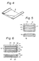
- Figure 4 illustrates the state where a plurality of etched foils 8 of a valve metal are superposed and on one side end, the foils 8 are integrated and electrically connected to the positive electrode terminal 7.
- the solid electrolytic capacitor of the second type is a capacitor formed of so-called polar type superposed foils.
- Figure 5 shows the section of a typical capacitor of the polar superposed foil type, which comprises foils 18, ... on the negative electrode side and foils 19, ... on the positive electrode side, which are alternatively superposed in parallel.
- the foils 18, ... on the negative electrode side are connected to a negative electrode terminal 17, and the foils 19, ... on the positive electrode side are connected to a positive electrode terminal 12.
- Figure 6 shows the section of a typical capacitor of the polar superposed foil type wherein a separator 20, a laminate 18 on the negative electrode side, a separator 20, a foil 19 on the positive electrode side, a separator 20, a foil 18 on the negative electrode side, ... are superposed in sequence and in parallel.
- the foils 18 on the negative electrode side are connected to a negative electrode terminal 17 and the foils 19 on the positive electrode side are connected to a positive electrode terminal 12.
- Figure 7 shows the section of the polar solid electrolytic capacitor of the second type according to the present invention
- Fig. 8 shows the section of a polar solid electrolytic capacitor including separators according to the present invention.
- Fig. 7 four foils 18 on the negative electrode side are connected electrically with the negative electrode terminal 17 and superposed and integrated with one another, and similarly, three foils 19 on the positive electrode side are connected electrically with the positive electrode terminal 12 and superposed and integrated with one another.
- the number of foils 18 on the negative electrode side and the number of foils 19 on the positive electrode side are not limited to those shown in Fig. 7, but may be decided according to need.
- the foils 18 on the negative electrode side and the foils 19 on the positive electrode side are alternatively superposed one upon the other, and a semiconductor layer 13 is formed between oxide film layers 21 formed on the surfaces of the foils 18 and 19.
- the structure shown in Fig. 8 is the same as the structure shown in Fig.
- the oxide film layers 21 may be damaged by the contact between the foils 18 and 19 on the negative electrode and positive electrode sides. Accordingly, preferably the separators are interposed in the above-mentioned manner.
- the solid electrolytic capacitor of the third type is a capacitor composed of bipolar type superposed foils.
- Fig. 9 shows the section of a bipolar solid electrolytic capacitor of the third type according to the present invention
- Fig. 10 shows the section of a bipolar type solid electrolytic capacitor including separators according to the present invention.
- capacitor structure shown in Fig. 9 is similar to the structure shown in Fig. 7, an oxide film layer 21 is formed on the surface of each of the respective foils 23 and 25 connected to both lead terminals 24 and 26, respectively.
- This capacitor can be used as a non-polar capacitor.
- the structure shown in Fig. 10 is the same as the structure shown in Fig. 9 except that a separator 20 is interposed between adjacent foils 23 and 25 extending from the lead terminals 24 and 26.
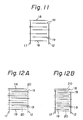
- Figure 11 is a diagram illustrating the section formed by alternately superposing foils 18 on the negative electrode side and foils 19 on the positive electrode side one upon the other.
- Figures 12A and 12B are diagrams illustrating the section formed by superposing foils 18 on the negative electrode side and foils 19 on the positive electrode side one upon the other interposing a separator 20 between each adjacent foil 18 and 19.
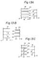
- Figure 13A is a sectional diagram illustrating an embodiment in which one separator 20 is interposed between two foils 18 on the negative electrode side, in the state where the separator 20 is folded on the side of the negative electrode terminal 17 and the foil 19 on the positive electrode side is inserted between the folds of the separator 20.
- Figure 13B is a sectional diagram illustrating an embodiment in which one separator 20 is interposed between two foils 19 on the positive electrode side, in the state where the separator 20 is folded on the side of the positive electrode terminal 12 and the foil 18 is interposed between the folds of the separator 20.
- Figure 13C is a sectional diagram illustrating an embodiment in which each foil 18 on the negative electrode side is inserted between folds of one separator 20 and the end of the foil 18 on the side opposite to the negative electrode is wrapped with the folded portion of the separator 20.
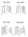
- Figure 13D is a sectional diagram illustrating an embodiment in which each foil 19 on the positive electrode side is inserted between folds of one separator 20 and the end of the foil 19 on the side opposite to the positive electrode is wrapped with the folded portion of the separator 20.
- Figure 13E is a sectional diagram illustrating an embodiment in which each foil 18 on the negative electrode side is inserted between two separators 20.
- Figure 13F is a sectional diagram illustrating an embodiment in which each foil 19 on the positive electrode side is inserted between two separators 20.
- FIG. 13G is a sectional diagram illustrating an embodiment in which one separator 20 is interposed for each of foils 18 on the negative electrode side and foils 19 on the positive electrode side.
- the separator on the outside of the outermost foil not superposed with the positive electrode may be present or may not be present as shown in Fig. 12A or 12B.
- the valve metal substrate is normally used as the positive electrode, and an oxide layer is formed thereon by electrolytic oxidation.
- a metal per se or a metal having a thin oxide layer formed thereon is used as the negative electrode.
- the foils are combined and separators are interposed in the same manner as described above with respect to the polar capacitor.
- a spacer 22 having a thickness almost equal to the thickness of the foil 19 on the positive electrode side may be interposed between foils 18 on the negative electrode side, and a spacer 22 having a thickness almost equal to the thickness of the foil 18 on the negative electrode side may be interposed between foils 19 on the positive electrode side. If this structure is adopted, the overlapping area between the foils 18 and 19 is increased, and therefore, this structure is preferable in order to ensure a sufficient capacitance in the capacitor. Furthermore, a modification may be adopted in which a spacer 22 is interposed for foils 18 on the negative electrode side or foils 19 on the positive electrode side, but a spacer is not disposed for the other foils.
- foils 18 on the negative electrode side and foils 19 on the positive electrode side may be combined without using a spacer 22, as shown in Fig. 14C.
- Any foil material can be used as the spacer 22.
- a metal foil to be used as the foil on the negative or positive electrode side may be used as the spacer 22, but superposed foils having an oxide film must be made of an insulating material or an electroconductive material, the surface of which is covered with an insulating film.
- isolation of the foils can be prevented by taping or the like.
- Figures 15A, 15B and 15C diagrammatically illustrate embodiments corresponding to Figs. 14A, 14B and 14C, respectively, in which separators 20 are interposed between foils 18 on the negative electrode side and foils 19 on the positive electrode side.
- valve metal substrate for the positive electrode in the solid electrolytic capacitor of the first or second type (polar type) according to the present invention there can be mentioned aluminum, tantalum, niobium, titanium and alloys composed mainly thereof.
- polar type polar type
- any of the above-mentioned valve metals can be used for each foil connected to both lead terminals. In general, the same metal is used for both foils.
- the oxide film layer on the surface of the positive electrode substrate or the negative electrode substrate may be either an oxide layer of the substrate per se or a layer of another dielectric oxide especially formed on the surface of the substrate.
- a layer composed of an oxide of the valve metal per se is preferred.
- an oxide film layer on the surface of the valve metal substrate is formed in the same manner as described above with respect to the polar type capacitor. In each type, a known method can be adopted for the formation of the oxide layer.
- an aluminum foil is used as the substrate
- the surface of the aluminum foils is electrochemically etched and then electrochemically treated in an aqueous solution of boric acid and ammonium borate, an oxide layer composed of an alumina dielectric material is formed on the aluminum foil as the substrate.
- the number of positive electrode foils is N (N is a positive integer) and the number of negative electrode foils is (N + 1).
- N is a positive integer
- N + 1 the number of negative electrode foils and the positive electrode foils.
- the foils are superposed and bound together according to a method such as caulking or high-frequency bonding, whereby the foils are electrically connected to the terminal, and where a separator is interposed between the negative electrode foil and the positive electrode foil, the foils are superposed and bound together in the state where the separator is included.
- the composition of the semiconductor layer or the method for forming the semiconductor layer is not particularly critical.
- a semiconductor layer composed mainly of lead dioxide or lead dioxide and lead sulfate is formed according to a known chemical deposition method or electrochemical deposition method.
- the electroconductivity is larger than 10 ⁇ 1 S ⁇ cm ⁇ 1 and the equivalent series resistance is further reduced.
- the chemical deposition method there can be mentioned, for example, a method in which the semiconductor is chemically deposited from a solution containing a lead-containing compound and an oxidant.
- lead-containing compounds in which a lead atom is coordination-bonded or ion-bonded to a chelate-forming compound such as oxine, acetylacetone, pyromeconic acid, salicyclic acid, alizarin, polyvinyl acetate, a porphyrin compound, a crown compound or a cryptate compound, and lead citrate, lead acetate, basic lead acetate, lead chloride, lead bromide, lead perchlorate, lead chlorate, lead sulfate, lead silicon hexafluoride, lead bromate, lead borofluoride, lead acetate hydrate, and lead nitrate.
- An appropriate lead-containing compound is selected according to the solvent used for the reaction mother liquid. A mixture of two or more of the foregoing lead-containing compounds may be used.
- the concentration of the lead-containing compound in the reaction mother liquid is in the range of from the concentration giving a saturation solubility of 0.05 mole/l, preferably from the concentration giving a saturation solubility to 0.1 mole/l, especially preferably from the concentration giving a saturation solubility to 0.5 mole/l. If the concentration of the lead-containing compound in the reaction mother liquid is lower than 0.05 mole/l, a solid electrolytic capacitor having a good performance cannot be obtained. If the concentration of the lead-containing compound in the reaction mother liquid exceeds the saturation solubility, no advantage is obtained by addition of the excessive amount of the lead-containing compound.
- oxidant there can be mentioned, for example, quinone, chloranil, pyridine-N-oxide, dimethyl sulfoxide, chromic acid, potassium permanganate, selenium oxide, mercury acetate, vanadium oxide, sodium chlorate, ferric chloride, hydrogen peroxide, benzoyl peroxide, calcium hypochlorite, calcium chlorite, calcium chlorate and calcium perchlorate.
- An appropriate oxidant is selected according to the solvent. A mixture of two or more of the foregoing oxidants may be used.
- the oxidant is used in an amount of 0.1 to 5 moles per mole of the lead-containing compound. If the amount of the oxidant is larger than 5 moles per mole of the lead-containing compound, no economical advantage is obtained, and if the amount of the oxidant is smaller than 0.1 mole per mole of the lead-containing compound, a solid electrolytic capacitor having a good performance cannot be obtained.
- the means for forming a semiconductor layer composed mainly of lead dioxide there can be adopted, for example, a method in which a solution containing the lead-containing compound is mixed with a solution containing the oxidant to prepare a reaction mother liquid and a foil laminate is immersed in the reaction mother liquid to chemically deposit lead dioxide on the foil laminate.
- the electrolyte used for forming a semiconductor layer composed mainly of lead dioxide by electrolytic oxidation is an aqueous solution containing a lead ion or an organic solvent solution containing a lead ion.
- a known electrolytic substance may be incorporated into the electrolyte.
- any solvent capable of dissolving therein the above-mentioned compound giving a lead ion seed can be used.
- ethyl alcohol, glycerol, benzene, dioxane and chloroform can be mentioned.
- a mixture of two or more of the foregoing organic solvents may be used.
- an organic solvent having a compatibility with water may be used in the form of a mixture with water.
- the lead ion concentration in the electrolyte is 0.2 mole/l to the concentration giving a saturation solubility, preferably from 0.5 mole/l to the concentration giving a saturation solubility, especially preferably from 0.9 mole/l to the solution giving a saturation solubility. If the concentration of the lead ion exceeds the level giving a saturation solubility, no advantage is obtained by an addition of an excessive amount of the lead ion.
- the lead ion concentration is lower than 0.2 mole/l, because of a too low concentration of the lead ion in the electrolyte, a semiconductor layer of lead dioxide formed by electrolytic oxidation does not sufficiently adhere to the oxide layer of the positive electrode substrate, and only a solid electrolytic capacitor having a very small capacitance and a large loss coefficient is obtained.
- Electrolytic oxidation can be performed according to a known method such as constant current method, a constant voltage method or a pulse method, or by adopting the constant current method and constant voltage method alternately.
- Known electrolytic apparatus and operation procedures may be adopted for electrolytic oxidation.
- the time and temperature of electrolytic oxidation are changed according to the kind of the positive electrode substrate, the substantial area of the oxide film, the kind of the lead ion seed, and the electrolytic conditions and cannot be simply defined. Preferably the time and temperature are decided based on the results of preliminary experiments.
- the semiconductor layer is constructed by a layer composed mainly of lead dioxide acting inherently as the semiconductor and lead sulfate acting as an insulating substance, the leak current value of the capacitor can be reduced.
- the incorporation of lead sulfate reduces the electroconductivity of the semiconductor layer, and therefore, the loss coefficient value is increased, but a performance much higher than that of the conventional solid electrolytic capacitor can be maintained.
- the semiconductor layer is formed of a mixture of lead dioxide and lead sulfate, a good capacitor performance can be maintained within such a broad composition range that the amount of lead dioxide is 10 to 100 parts by weight and the amount of lead sulfate is up to 90 parts by weight.
- the semiconductor layer is composed of a mixture comprising 20 to 50% by weight, especially 25 to 35% by weight, of lead dioxide and 80 to 50% by weight, especially 75 to 65% by weight, of lead sulfate. If the content of lead dioxide is lower than 10% by weight, the electroconductivity is reduced and the loss coefficient value is increased, and a sufficient capacitance is not manifested.
- the semiconductor layer composed mainly of lead dioxide and lead sulfate can be prepared, for example, by chemical deposition using an aqueous solution containing a lead ion and a persulfate ion as the reaction mother liquid.
- An oxidant free of a persulfate ion may be added to the aqueous solution.
- the lead ion concentration in the mother liquid is from the concentration giving a saturation solubility to 0.05 mole/l, preferably from the concentration giving a saturation solubility to 0.1 mole/l, especially preferably from the concentration giving a saturation solubility to 0.5 mole/l. If the lead ion concentration exceeds the concentration giving a saturation solubility, no advantage is obtained by an addition of an excessive amount of the lead ion. If the lead ion concentration is lower than 0.05 mole/l, because of a too low lead ion concentration in the mother liquid, the frequency of deposition of the semiconductor should be increased.
- the persulfate ion concentration in the mother liquid is such that the molar ratio of the persulfate ion to the lead ion is from 5 to 0.05. If this molar ratio exceeds 5, the unreacted persulfate ion is left and the manufacturing cost is increased. If the molar ratio is lower than 0.05, the unreacted lead ion is left and the electroconductivity is reduced.
- the compound giving a lead ion seed there can be mentioned, for example, lead citrate, lead perchlorate, lead nitrate, lead acetate, basic lead acetate, lead chlorate, lead sulfamate, silicon lead hexafluoride, lead bromate, lead chloride, and lead bromide. A mixture of two or more of these compounds giving a lead ion seed may be used.
- the compound giving a persulfate ion seed there can be mentioned, for example, potassium persulfate, sodium persulfate and ammonium persulfate. A mixture of two or more of these compounds giving a persulfate ion seed may be used.
- oxidant there can be mentioned, for example, hydrogen peroxide, calcium hypochlorite, calcium chlorite, calcium chlorate and calcium perchlorate.
- the electroconductive layer on the semiconductor layer may be formed, for example, by solidification of an electroconductive paste, plating and metal vacuum deposition.
- an electroconductive paste there are preferably used a silver paste, a copper paste, a nickel paste, an aluminum paste and a carbon paste. These pastes may be used singly or in the form of mixtures of two or more thereof. If at least two pastes are used, they may be used in the form of a mixture, or in the form of a superposed layers. After the electroconductive paste is applied, the paste is allowed to stand in air or is heated, whereby the paste is solidified.
- plating there can be mentioned nickel plating, copper plating and aluminum plating.
- metal to be vacuum-deposited there can be mentioned aluminum and copper.
- the common negative electrode terminal may be attached by using an electroconductive paste or soldered onto the electroconductive layer.
- the assembly may be strengthened by taping or the like before or after attachment of the common negative electrode terminal.
- the solid electrolytic capacitor of the present invention has a very small equivalent series resistance in the high-frequency band region and a good performance, and the volume is very small.
- the solid electrolytic capacitor of the present invention can be used as a general-purpose capacitor in various fields with an exterior part such as a resin mold, a resin case, a metal case, resin dipping or a laminate film.
- Ten foil pieces having a length of 1 cm and a width of 0.5 cm were cut out from an aluminum foil electrochemically etched by an alternating current, and these ten pieces were superposed, a positive electrode terminal was caulked to one end of the superposed structure, and the foil pieces were electrically connected. Subsequently, the superposed assembly was electrically treated in an aqueous solution of boric acid and ammonium borate to form an aluminum oxide layer and obtain an assembly of ten formed etched aluminum foils (about 1 ⁇ F/cm2) for a low voltage, which were combined by the positive electrode terminal.
- the assembly of the formed foils was immersed in an aqueous solution containing 1 mole/l of lead acetate and a dilute aqueous solution containing hydrogen peroxide in an amount of 0.5 mole per mole of lead acetate was added to the above aqueous solution.
- the foils were allowed to stand for 1 hour in this state.
- the lead dioxide layer precipitated on the formed foil was washed with water and dried at 120°C under a reduced pressure.
- the formed foil having the lead dioxide layer deposited thereon was immersed in a silver paste bath, taken out therefrom and air-dried to form a solidified paste layer on the lead dioxide layer.
- the foils were bound together by taping along a width of 0.2 cm, and the end other than the end connected to the positive electrode terminal was left free. Then the end other than the end connected to the positive electrode terminal was immersed in a soldering bath and a common negative electrode terminal was connected to the free end. The assembly was then sealed with a resin to form a solid electrolytic capacitor.
- the superposed formed foils prepared in the same manner as described in Example 1 were immersed in an aqueous solution containing 1.9 mole/l of lead nitrate, except a part of the positive electrode terminal. Electrolytic oxidation was carried out at a constant current for 10 hours by using carbon as the negative electrode to form a lead dioxide layer on the formed foil. Then, the formed foil was taken out, washed with water and dried at 100°C under a reduced pressure for 1 hour. A solid electrolytic capacitor was then prepared in the same manner as described in Example 1.
- Example 2 An aqueous solution containing 3.8 mole/l of lead acetate trihydrate and an aqueous solution containing 4.0 mole/l of ammonium persulfate, each maintained at 50°C, were mixed, and the same formed foils as used in Example 1 were immersed in this mixed liquid and allowed to stand at 80°C for 20 minutes.
- the semiconductor layers precipitated on the formed foils were washed with water to remove the unreacted substance and the foil were dried at 120°C for 1 hour under a reduced pressure.
- the formed semiconductor layer consisted of lead dioxide and lead sulfate. By mass analysis, X-ray analysis and infrared spectrum analysis, it was confirmed that the semiconductor layer contained about 25% by weight of lead dioxide.
- a solid electrolytic capacitor was then prepared in the same manner as described in Example 1.
- a solid electrolytic capacitor was prepared in the same manner as described in Example 3 except that the concentration of ammonium persulfate was changed to 0.3 mole/l at the step of forming the semiconductor layer. It was confirmed that the semiconductor layer consisted of lead dioxide and lead sulfate and the content of lead dioxide was about 35% by weight.
- a solid electrolytic capacitor was prepared in the same manner as described in Example 3 except that aqueous hydrogen peroxide having a concentration of 0.05 mole/l was added at the step of forming the semiconductor layer. It was confirmed that the semiconductor layer consisted of lead dioxide and lead sulfate and the content of lead dioxide was 50% by weight.
- An oxide film was formed on a known sintered body of aluminum powder as the positive electrode substrate, and the operation of immersion in an aqueous solution of manganese nitrate and thermal decomposition was carried out 3 times to form a semiconductor composed of manganese dioxide. Then, a carbon paste and a silver paste were applied and dried, and the assembly was immersed in a soldering bath and sealed with a resin to obtain a solid electrolytic capacitor.
- the superposed assembly was electrochemically treated in an aqueous solution of boric acid and ammonium borate to form an aluminum oxide layer and obtain an assembly of four formed etched aluminum foils (about 1 ⁇ F/cm2) for a low voltage, which were connected by the positive electrode terminal. Subsequently, the formed etched aluminum foils as the positive electrode were inserted one by one between the above-mentioned integrated negative electrode foils to form an assembly in which the positive electrode foils and the negative electrode foils were alternately superposed. A part of the assembly was bound by taping to prevent deviation of the positions of the negative electrode foils.
- the assembly was immersed in an aqueous solution containing 1 mole/l of lead acetate and a dilute aqueous solution containing hydrogen peroxide in an amount of 0.5 mole per mole of lead acetate was added to the above aqueous solution.
- the assembly was allowed to stand for 1 hour in this state.
- the lead dioxide layer precipitated on the assembly was washed with water and dried at 120°C under a reduced pressure. This operation was repeated 2 times, and the assembly was sealed with a resin except the terminal portions to obtain a solid electrolytic capacitor.
- the formed etched aluminum foils as the positive electrode were inserted one by one between the above-mentioned partially integrated foils as the negative electrode to form an assembly in which the foils as the positive electrode and the foils as the negative electrode were alternately superposed in parallel.
- a lead dioxide layer was formed on the assembly and the assembly was post-treated to obtain a solid electrolytic capacitor.
- a solid electrolytic capacitor was prepared in the same manner as described in Example 6 except that a liquid mixture of an aqueous solution containing 3.8 mole/l of lead acetate trihydrate and an aqueous solution containing 4.0 mole/l of ammonium persulfate was used as the solution for formation of the semiconductor layer.
- a liquid mixture of an aqueous solution containing 3.8 mole/l of lead acetate trihydrate and an aqueous solution containing 4.0 mole/l of ammonium persulfate was used as the solution for formation of the semiconductor layer.
- a solid electrolytic capacitor was prepared in the same manner as described in Example 7 except that rayon separators were used instead of the polypropylene nets and a liquid mixture of an aqueous solution containing 3.8 mole/l of lead acetate trihydrate and an aqueous solution containing 4.0 mole/l of ammonium persulfate was used as the solution for formation of the semiconductor layer.
- rayon separators were used instead of the polypropylene nets and a liquid mixture of an aqueous solution containing 3.8 mole/l of lead acetate trihydrate and an aqueous solution containing 4.0 mole/l of ammonium persulfate was used as the solution for formation of the semiconductor layer.
- a liquid mixture of an aqueous solution containing 3.8 mole/l of lead acetate trihydrate and an aqueous solution containing 4.0 mole/l of ammonium persulfate was used as the solution for formation of the semiconductor layer.
- a solid electrolytic capacitor was prepared in the same manner as described in Example 8 except that aqueous hydrogen peroxide having a concentration of 0.05 mole/l was added at the step of forming the semiconductor layer. It was confirmed that the semiconductor consisted of lead dioxide and lead sulfate and the content of the lead dioxide was about 50% by weight.
- a solid electrolytic capacitor was prepared in the same manner as described in Example 9 except that aqueous hydrogen peroxide having a concentration of 0.05 mole/l was added at the step of forming the semiconductor layer. It was confirmed that the semiconductor layer consisted of lead dioxide and lead sulfate and the content of lead dioxide was about 50% by weight.
- a solid electrolytic capacitor was prepared in the same manner as described in Example 8 except that aluminum foils having a length of 0.1 cm and an aluminum foil of 0.5 cm were integrated as spacers at the step of forming the partially integrated assembly of the formed aluminum foils.
- a solid electrolytic capacitor was prepared in the same manner as described in Example 9 except that aluminum foils having a length of 0.1 cm and a width of 0.5 cm were incorporated as spacers at the step of forming the partially integrated assembly of the formed aluminum foils.
- a solid electrolytic capacitor was prepared in the same manner as that in Comparative Example 1 except that a sintered body of aluminum powder having a smaller size was adopted.
Landscapes
- Engineering & Computer Science (AREA)
- Power Engineering (AREA)
- Microelectronics & Electronic Packaging (AREA)
- Fixed Capacitors And Capacitor Manufacturing Machines (AREA)
Description
- The present invention relates to a solid electrolytic capacitor of the superposed foil type having a good performance.
- A metal having a valve action (hereinafter referred to as "valve metal"), such as tantalum, aluminum, niobium or titanium, is used as a positive electrode substrate of the conventional solid electrolytic capacitor. Of these, tantalum and aluminum are often adopted.
- For example, a solid electrolytic capacitor comprising aluminum as the positive electrode substrate has a section as shown in Fig. 1. Referring to Fig. 1, an aluminum oxide film which is a dielectric substance is formed on the surface of a sintered body of aluminum powder to form a
positive electrode substrate 2. A semiconductor layer 3 is formed on this aluminum oxide film andelectroconductive layers reference numerals 1 and 6 represent a positive electrode terminal and a solder layer, respectively. - However, the conventional solid electrolytic capacitor has problems in that, since thermal decomposition is carried out several times in the preparation process, the preparation steps become complicated, and the equivalent series resistance in the high-frequency band region is too large.
- FR-A-2462775 discloses a solid electrolyte capacitor comprising a plurality of superposed aluminum foils having an aluminum oxide film layer, a semiconductor layer formed on the oxide film layer, and electroconductive layers formed on the semiconductor layer.
- DE-A-1205193 discloses a solid electrolyte capacitor comprising an aluminum electrode having semiconductor layers formed on both sides thereof and current supply electrodes in register therewith and each having two mutually apposite connection lugs.
- In the solid electrolyte capacitors of the two immediately preceding prior art documents, the aluminum electrode or foil has a portion on which the semiconductor layer is not formed.
- Under this background, it is a primary object of the present invention to provide a superior solid electrolytic capacitor having a small equivalent series resistance in the high-frequency band region and having an enhanced capacitance per unit volume.
- In accordance with one fundamental aspect of the present invention, there is provided a solid electrolytic capacitor comprising a plurality of superposed etched foils of a valve metal each having an oxide film surface layer, which are electrically connected with a positive electrode terminal, a semiconductor layer formed on the oxide film layer, an electroconductive layer formed on the semiconductor layer, and a negative electrode terminal common to the respective foils, which is formed on the electroconductive layer, characterised in that the valve metal foils each having an oxide film surface layer and interconnection points between the valve metal foils and the positive electrode terminal are embedded in the semiconductor layer, and the semiconductor layer is embedded in the electroconductive layer (this solid electrolytic capacitor hereinafter referred to as "solid electrolytic capacitor of the first type").
- Further, according to the present invention there is provided a process for making an electrolytic capacitor according to the "first type" wherein:
the superposed etched valve metal foils each having an oxide film surface layer, which are electrically connected with the positive electrode terminal, is immersed in a liquid containing a lead-containing compound to form a semiconductor layer such that the valve metal foils and the interconnecting points between the valve metal foils and the positive electrode terminal are embedded in the semiconductor layer;
the valve metal foils and the positive electrode terminal, which have been embedded in the semiconductor layer, are immersed in a paste of an electroconductive material, plated with an electroconductive material, or vacuum-deposited with an electroconductive material, so that a layer of the electroconductive material is formed on the entire surface of the semiconductor layer; and
the negative electrode terminal is attached to the thus-formed electroconductive layer. - In accordance with another aspect of the present invention, there is provided a solid electrolytic capacitor having a structure in which a plurality of first foils electrically connected with a negative electrode terminal and a plurality of second foils of a valve metal each having an oxide film surface layer on the surface thereof, which are electrically connected with a positive electrode terminal, are alternately superposed one upon the other, characterised in that the first valve metal foils, interconnection points between the first valve metal foils and the negative electrode terminal, the second valve metal foils each having the oxide film layer, and interconnection points between the second valve metal foils and the positive electrode terminal are embedded in a semiconductor layer (this solid electrolytic capacitor is hereinafter referred to as "solid electrolytic capacitor of the second type").
- Further, according to the present invention there is provided a process for making an electrolytic capacitor according to the "second type" wherein:
the plurality of first foils electrically connected with a negative electrode terminal and the plurality of second valve metal foils each having the oxide film surface layer, which are electrically connected with the positive electrode terminal, are alternately superposed one upon the other; and
the thus-prepared assembly of the first foils, the negative electrode terminal, the second valve metal foils, and the positive electrode terminal is immersed in a liquid containing a lead-containing compound to form a semiconductor layer such that the first foils, interconnecting points between the first foils and the negative electrode terminal, the second valve metal foils, and interconnecting points between the second valve metal foils and the positive electrode terminal are embedded in the semiconductor layer. - In accordance with still another aspect of the present invention, there is provided a solid electrolytic capacitor having a structure in which a plurality of first foils of a valve metal each having an oxide film layer on the surface thereof, which are electrically connected with one lead terminal, and a plurality of second foils of a valve metal each haing an oxide film layer on the surface thereof, which are electrically connected with the other lead terminal, are alternately superposed one upon the other, characterised in that the first valve metal foils each having the oxide film layer, interconnecting points between the first valve metal foils and the lead terminal, the second valve metal foils each having the oxide film layer, and interconnecting points between the second valve metal foils and the lead terminal are embedded in a semiconductor layer (this solid electrolytic capacitor hereinafter referred to as "solid electrolytic capacitor of the third type").
- Further, according to the present invention there is provided a process for making an electrolytic capacitor according to the "third type" wherein:
the plurality of first valve metal foils each having an oxide film layer, which are electrically connected with the lead terminal, and the plurality of second valve metal foils each having an oxide film layer, which are electrically connected with the other lead terminal, are alternately superposed one upon the other; and
the thus-prepared assembly of the first valve metal foils, the lead terminal, the second valve metal foils, and the lead terminal is immersed in the liquid containing a lead-containing compound to prepare a semiconductor layer such that the first valve metal foils, interconnecting points between the first valve metal foils and the lead terminal, the second valve metal foils, and interconnecting points between the second valve metal foils and the lead terminal are embedded in the semiconductor layer. -
- Fig. 1 is a sectional view illustrating a conventional solid electrolytic capacitor;
- Fig. 2 is an equivalent circuit diagram of a solid electrolytic capacitor according to the present invention;
- Fig. 3 is a sectional view illustrating a solid electrolytic capacitor of the first type according to the present invention;
- Fig. 4 is a perspective view illustrating a superposed positive electrode substrates used for a solid electrolytic capacitor of the first type according to the present invention;
- Fig. 5 is a sectional view illustrating the superposed structure is a polar type solid electrolytic capacitor;
- Fig. 6 is a sectional view illustrating the superposed structure of a solid electrolytic capacitor including a separator;
- Fig. 7 is a sectional view illustrating a solid electrolytic capacitor of the second type (i.e., polar type) according to the present invention;
- Fig. 8 is a sectional view illustrating a solid electrolytic capacitor of the second type (i.e., polar type) including separators according to the present invention;
- Fig. 9 is a sectional view illustrating a solid electrolytic capacitor of the third type (i.e., bipolar type) according to the present invention;
- Fig.10 is a sectional view illustrating a solid electrolytic capacitor of the third type (i.e., bipolar type) including separators according to the present invention;
- Fig. 11 is a sectional diagram illustrating a combination of foils on the negative electrode side and the positive electrode side in a solid electrolytic capacitor of the polar type;
- Figs. 12A and 12B are sectional diagrams illustrating combinations of foils on the negative electrode side and the positive electrode side in a solid electrolytic capacitor of the polar type;
- Figs. 13A through 13G are sectional diagrams illustrating combinations of foils on the negative electrode side and the positive electrode side in a solid electrolytic capacitor of the polar type including a separator;
- Figs. 14A and 14B are sectional diagrams illustrating the state of interposition of spacers and the presence of spaces between electrode foils, and Fig. 14C is a sectional diagram illustrating the same combination of foils as that shown in Fig. 14B except that spacers are not interposed; and,
- Figs. 15A through 15C are sectional views similar to Figs. 14A through 14C in a solid electrolytic capacitor of the polar type including separators.
- The solid electrolytic capacitor of the present invention has a superposed foil structure, irrespective of type. Accordingly, as shown in Fig. 2, the synthetic resistance value of the equivalent circuit of the solid electrolytic capacitor of the present invention is 1/N (N is the number of foils of each electrode) and the equivalent series resistance value in the high-frequency band region is very small. Furthermore, the preparation process is very simple and thus is industrially advantageous.
- The section of a typical example of the solid electrolytic capacitor of the first type according to the present invention is shown in Fig. 3. As shown in Fig. 3, a plurality (three in Fig. 3) of
etched foils 8 having an oxide film surface layer are piled and on one side end, thefoils 8 of valve metal are integrated and electrically connected with apositive electrode terminal 7. Asemiconductor layer 9 is formed on the oxide film layer of eachfoil 8, anelectroconductive layer 10 is formed on thesemiconductor layer 9, and a commonnegative electrode terminal 11 is formed on theelectroconductive layer 10. - Figure 4 illustrates the state where a plurality of
etched foils 8 of a valve metal are superposed and on one side end, thefoils 8 are integrated and electrically connected to thepositive electrode terminal 7. - The solid electrolytic capacitor of the second type is a capacitor formed of so-called polar type superposed foils.
- Figure 5 shows the section of a typical capacitor of the polar superposed foil type, which comprises
foils 18, ... on the negative electrode side andfoils 19, ... on the positive electrode side, which are alternatively superposed in parallel. Thefoils 18, ... on the negative electrode side are connected to anegative electrode terminal 17, and thefoils 19, ... on the positive electrode side are connected to apositive electrode terminal 12. Figure 6 shows the section of a typical capacitor of the polar superposed foil type wherein aseparator 20, a laminate 18 on the negative electrode side, aseparator 20, afoil 19 on the positive electrode side, aseparator 20, afoil 18 on the negative electrode side, ... are superposed in sequence and in parallel. The foils 18 on the negative electrode side are connected to anegative electrode terminal 17 and thefoils 19 on the positive electrode side are connected to apositive electrode terminal 12. - Figure 7 shows the section of the polar solid electrolytic capacitor of the second type according to the present invention, and Fig. 8 shows the section of a polar solid electrolytic capacitor including separators according to the present invention.
- In Fig. 7, four foils 18 on the negative electrode side are connected electrically with the
negative electrode terminal 17 and superposed and integrated with one another, and similarly, three foils 19 on the positive electrode side are connected electrically with thepositive electrode terminal 12 and superposed and integrated with one another. The number offoils 18 on the negative electrode side and the number offoils 19 on the positive electrode side are not limited to those shown in Fig. 7, but may be decided according to need. The foils 18 on the negative electrode side and thefoils 19 on the positive electrode side are alternatively superposed one upon the other, and asemiconductor layer 13 is formed between oxide film layers 21 formed on the surfaces of thefoils separator 20 is interposed between eachadjacent foil foils - The solid electrolytic capacitor of the third type is a capacitor composed of bipolar type superposed foils.
- Fig. 9 shows the section of a bipolar solid electrolytic capacitor of the third type according to the present invention, and Fig. 10 shows the section of a bipolar type solid electrolytic capacitor including separators according to the present invention.
- Although the capacitor structure shown in Fig. 9 is similar to the structure shown in Fig. 7, an
oxide film layer 21 is formed on the surface of each of the respective foils 23 and 25 connected to bothlead terminals separator 20 is interposed betweenadjacent foils lead terminals - The method for integrating superposed foils and interposing separators will now be described with reference to a solid electrolytic capacitor of the polar type.
- Figure 11 is a diagram illustrating the section formed by alternately superposing foils 18 on the negative electrode side and foils 19 on the positive electrode side one upon the other. Figures 12A and 12B are diagrams illustrating the section formed by superposing foils 18 on the negative electrode side and foils 19 on the positive electrode side one upon the other interposing a
separator 20 between eachadjacent foil - Figure 13A is a sectional diagram illustrating an embodiment in which one
separator 20 is interposed between twofoils 18 on the negative electrode side, in the state where theseparator 20 is folded on the side of thenegative electrode terminal 17 and thefoil 19 on the positive electrode side is inserted between the folds of theseparator 20. Figure 13B is a sectional diagram illustrating an embodiment in which oneseparator 20 is interposed between twofoils 19 on the positive electrode side, in the state where theseparator 20 is folded on the side of thepositive electrode terminal 12 and thefoil 18 is interposed between the folds of theseparator 20. Figure 13C is a sectional diagram illustrating an embodiment in which eachfoil 18 on the negative electrode side is inserted between folds of oneseparator 20 and the end of thefoil 18 on the side opposite to the negative electrode is wrapped with the folded portion of theseparator 20. Figure 13D is a sectional diagram illustrating an embodiment in which eachfoil 19 on the positive electrode side is inserted between folds of oneseparator 20 and the end of thefoil 19 on the side opposite to the positive electrode is wrapped with the folded portion of theseparator 20. Figure 13E is a sectional diagram illustrating an embodiment in which eachfoil 18 on the negative electrode side is inserted between twoseparators 20. Figure 13F is a sectional diagram illustrating an embodiment in which eachfoil 19 on the positive electrode side is inserted between twoseparators 20. Fig. 13G is a sectional diagram illustrating an embodiment in which oneseparator 20 is interposed for each of foils 18 on the negative electrode side and foils 19 on the positive electrode side. In each of the embodiments shown in Figs. 13A through 13G, the separator on the outside of the outermost foil not superposed with the positive electrode may be present or may not be present as shown in Fig. 12A or 12B. - The valve metal substrate is normally used as the positive electrode, and an oxide layer is formed thereon by electrolytic oxidation. A metal per se or a metal having a thin oxide layer formed thereon is used as the negative electrode.
- Also, in the bipolar capacitors of the first and second types, the foils are combined and separators are interposed in the same manner as described above with respect to the polar capacitor.
- In the polar capacitor of the second type, as shown in Fig. 14A, a
spacer 22 having a thickness almost equal to the thickness of thefoil 19 on the positive electrode side may be interposed betweenfoils 18 on the negative electrode side, and aspacer 22 having a thickness almost equal to the thickness of thefoil 18 on the negative electrode side may be interposed betweenfoils 19 on the positive electrode side. If this structure is adopted, the overlapping area between thefoils spacer 22 is interposed forfoils 18 on the negative electrode side or foils 19 on the positive electrode side, but a spacer is not disposed for the other foils. Moreover, foils 18 on the negative electrode side and foils 19 on the positive electrode side may be combined without using aspacer 22, as shown in Fig. 14C. Any foil material can be used as thespacer 22. A metal foil to be used as the foil on the negative or positive electrode side may be used as thespacer 22, but superposed foils having an oxide film must be made of an insulating material or an electroconductive material, the surface of which is covered with an insulating film. In order to strengthen a superposed assembly of positive electrode foils and negative electrode foils, isolation of the foils can be prevented by taping or the like. - Figures 15A, 15B and 15C diagrammatically illustrate embodiments corresponding to Figs. 14A, 14B and 14C, respectively, in which separators 20 are interposed between
foils 18 on the negative electrode side and foils 19 on the positive electrode side. - Methods similar to the methods described above with respect to the polar capacitor may be applied to the preparation of the bipolar capacitor.
- Any metal having a valve action can be used as the valve metal substrate for the positive electrode in the solid electrolytic capacitor of the first or second type (polar type) according to the present invention. For example, there can be mentioned aluminum, tantalum, niobium, titanium and alloys composed mainly thereof. In the capacitor of the third type (bipolar type) according to the present invention, any of the above-mentioned valve metals can be used for each foil connected to both lead terminals. In general, the same metal is used for both foils.
- From the practical viewpoint, aluminum is most preferred among the foregoing metals.
- In the capacitor of the first or second type (polar type) according to the present invention, the oxide film layer on the surface of the positive electrode substrate or the negative electrode substrate may be either an oxide layer of the substrate per se or a layer of another dielectric oxide especially formed on the surface of the substrate. A layer composed of an oxide of the valve metal per se is preferred. Also in the bipolar type capacitor, an oxide film layer on the surface of the valve metal substrate is formed in the same manner as described above with respect to the polar type capacitor. In each type, a known method can be adopted for the formation of the oxide layer.
- For example, where an aluminum foil is used as the substrate, if the surface of the aluminum foils is electrochemically etched and then electrochemically treated in an aqueous solution of boric acid and ammonium borate, an oxide layer composed of an alumina dielectric material is formed on the aluminum foil as the substrate.
- In the polar type capacitor, the number of positive electrode foils is N (N is a positive integer) and the number of negative electrode foils is (N + 1). However, where negative electrode superposed foils and positive electrode superposed foils are commonly prepared, the number of each of the negative electrode foils and the positive electrode foils is N, and although the capacitance per se is somewhat smaller than in the above-mentioned combination, the production efficiency is increased. Accordingly, N number of negative electrode foils and N number of positive electrode foils may be used in combination.
- Before or after formation of the oxide film layer, the foils are superposed and bound together according to a method such as caulking or high-frequency bonding, whereby the foils are electrically connected to the terminal, and where a separator is interposed between the negative electrode foil and the positive electrode foil, the foils are superposed and bound together in the state where the separator is included.
- In the present invention, the composition of the semiconductor layer or the method for forming the semiconductor layer is not particularly critical. However, in order to increase the performance of the capacitor, preferably a semiconductor layer composed mainly of lead dioxide or lead dioxide and lead sulfate is formed according to a known chemical deposition method or electrochemical deposition method. In the semiconductor layer composed mainly of lead dioxide or lead dioxide and lead sulfate, the electroconductivity is larger than 10⁻¹ S·cm⁻¹ and the equivalent series resistance is further reduced.
- As the chemical deposition method, there can be mentioned, for example, a method in which the semiconductor is chemically deposited from a solution containing a lead-containing compound and an oxidant.
- As the lead-containing compound, there can be mentioned lead-containing compounds in which a lead atom is coordination-bonded or ion-bonded to a chelate-forming compound such as oxine, acetylacetone, pyromeconic acid, salicyclic acid, alizarin, polyvinyl acetate, a porphyrin compound, a crown compound or a cryptate compound, and lead citrate, lead acetate, basic lead acetate, lead chloride, lead bromide, lead perchlorate, lead chlorate, lead sulfate, lead silicon hexafluoride, lead bromate, lead borofluoride, lead acetate hydrate, and lead nitrate. An appropriate lead-containing compound is selected according to the solvent used for the reaction mother liquid. A mixture of two or more of the foregoing lead-containing compounds may be used.
- The concentration of the lead-containing compound in the reaction mother liquid is in the range of from the concentration giving a saturation solubility of 0.05 mole/ℓ, preferably from the concentration giving a saturation solubility to 0.1 mole/ℓ, especially preferably from the concentration giving a saturation solubility to 0.5 mole/ℓ. If the concentration of the lead-containing compound in the reaction mother liquid is lower than 0.05 mole/ℓ, a solid electrolytic capacitor having a good performance cannot be obtained. If the concentration of the lead-containing compound in the reaction mother liquid exceeds the saturation solubility, no advantage is obtained by addition of the excessive amount of the lead-containing compound.
- As the oxidant, there can be mentioned, for example, quinone, chloranil, pyridine-N-oxide, dimethyl sulfoxide, chromic acid, potassium permanganate, selenium oxide, mercury acetate, vanadium oxide, sodium chlorate, ferric chloride, hydrogen peroxide, benzoyl peroxide, calcium hypochlorite, calcium chlorite, calcium chlorate and calcium perchlorate. An appropriate oxidant is selected according to the solvent. A mixture of two or more of the foregoing oxidants may be used.
- Preferably the oxidant is used in an amount of 0.1 to 5 moles per mole of the lead-containing compound. If the amount of the oxidant is larger than 5 moles per mole of the lead-containing compound, no economical advantage is obtained, and if the amount of the oxidant is smaller than 0.1 mole per mole of the lead-containing compound, a solid electrolytic capacitor having a good performance cannot be obtained.
- As the means for forming a semiconductor layer composed mainly of lead dioxide, there can be adopted, for example, a method in which a solution containing the lead-containing compound is mixed with a solution containing the oxidant to prepare a reaction mother liquid and a foil laminate is immersed in the reaction mother liquid to chemically deposit lead dioxide on the foil laminate.
- As the electrochemical deposition method, there can be mentioned a method previously proposed by us, in which lead dioxide is deposited by electrolytic oxidation in an electrolyte containing a lead ion at a high concentration (see Japanese Unexamined Patent Publication No. 62-185307).
- The electrolyte used for forming a semiconductor layer composed mainly of lead dioxide by electrolytic oxidation is an aqueous solution containing a lead ion or an organic solvent solution containing a lead ion. In order to improve the ion electroconductivity of the electrolyte, a known electrolytic substance may be incorporated into the electrolyte.
- As the organic solvent used for formation of the organic solvent solution, any solvent capable of dissolving therein the above-mentioned compound giving a lead ion seed can be used. For example, there can be mentioned ethyl alcohol, glycerol, benzene, dioxane and chloroform. A mixture of two or more of the foregoing organic solvents may be used. Furthermore, an organic solvent having a compatibility with water may be used in the form of a mixture with water.
- The lead ion concentration in the electrolyte is 0.2 mole/ℓ to the concentration giving a saturation solubility, preferably from 0.5 mole/ℓ to the concentration giving a saturation solubility, especially preferably from 0.9 mole/ℓ to the solution giving a saturation solubility. If the concentration of the lead ion exceeds the level giving a saturation solubility, no advantage is obtained by an addition of an excessive amount of the lead ion. If the lead ion concentration is lower than 0.2 mole/ℓ, because of a too low concentration of the lead ion in the electrolyte, a semiconductor layer of lead dioxide formed by electrolytic oxidation does not sufficiently adhere to the oxide layer of the positive electrode substrate, and only a solid electrolytic capacitor having a very small capacitance and a large loss coefficient is obtained.
- Electrolytic oxidation can be performed according to a known method such as constant current method, a constant voltage method or a pulse method, or by adopting the constant current method and constant voltage method alternately. Known electrolytic apparatus and operation procedures may be adopted for electrolytic oxidation. The time and temperature of electrolytic oxidation are changed according to the kind of the positive electrode substrate, the substantial area of the oxide film, the kind of the lead ion seed, and the electrolytic conditions and cannot be simply defined. Preferably the time and temperature are decided based on the results of preliminary experiments.
- If the semiconductor layer is constructed by a layer composed mainly of lead dioxide acting inherently as the semiconductor and lead sulfate acting as an insulating substance, the leak current value of the capacitor can be reduced. On the other hand, the incorporation of lead sulfate reduces the electroconductivity of the semiconductor layer, and therefore, the loss coefficient value is increased, but a performance much higher than that of the conventional solid electrolytic capacitor can be maintained. Namely, if the semiconductor layer is formed of a mixture of lead dioxide and lead sulfate, a good capacitor performance can be maintained within such a broad composition range that the amount of lead dioxide is 10 to 100 parts by weight and the amount of lead sulfate is up to 90 parts by weight. In order to obtain a good balance between the leak current value and the loss coefficient value, preferably the semiconductor layer is composed of a mixture comprising 20 to 50% by weight, especially 25 to 35% by weight, of lead dioxide and 80 to 50% by weight, especially 75 to 65% by weight, of lead sulfate. If the content of lead dioxide is lower than 10% by weight, the electroconductivity is reduced and the loss coefficient value is increased, and a sufficient capacitance is not manifested.
- The semiconductor layer composed mainly of lead dioxide and lead sulfate can be prepared, for example, by chemical deposition using an aqueous solution containing a lead ion and a persulfate ion as the reaction mother liquid. An oxidant free of a persulfate ion may be added to the aqueous solution.
- The lead ion concentration in the mother liquid is from the concentration giving a saturation solubility to 0.05 mole/ℓ, preferably from the concentration giving a saturation solubility to 0.1 mole/ℓ, especially preferably from the concentration giving a saturation solubility to 0.5 mole/ℓ. If the lead ion concentration exceeds the concentration giving a saturation solubility, no advantage is obtained by an addition of an excessive amount of the lead ion. If the lead ion concentration is lower than 0.05 mole/ℓ, because of a too low lead ion concentration in the mother liquid, the frequency of deposition of the semiconductor should be increased.
- The persulfate ion concentration in the mother liquid is such that the molar ratio of the persulfate ion to the lead ion is from 5 to 0.05. If this molar ratio exceeds 5, the unreacted persulfate ion is left and the manufacturing cost is increased. If the molar ratio is lower than 0.05, the unreacted lead ion is left and the electroconductivity is reduced.
- As the compound giving a lead ion seed, there can be mentioned, for example, lead citrate, lead perchlorate, lead nitrate, lead acetate, basic lead acetate, lead chlorate, lead sulfamate, silicon lead hexafluoride, lead bromate, lead chloride, and lead bromide. A mixture of two or more of these compounds giving a lead ion seed may be used. As the compound giving a persulfate ion seed, there can be mentioned, for example, potassium persulfate, sodium persulfate and ammonium persulfate. A mixture of two or more of these compounds giving a persulfate ion seed may be used.
- As the oxidant, there can be mentioned, for example, hydrogen peroxide, calcium hypochlorite, calcium chlorite, calcium chlorate and calcium perchlorate.
- In the solid electrolytic capacitor of the first type according to the present invention, the electroconductive layer on the semiconductor layer may be formed, for example, by solidification of an electroconductive paste, plating and metal vacuum deposition. As the electroconductive paste, there are preferably used a silver paste, a copper paste, a nickel paste, an aluminum paste and a carbon paste. These pastes may be used singly or in the form of mixtures of two or more thereof. If at least two pastes are used, they may be used in the form of a mixture, or in the form of a superposed layers. After the electroconductive paste is applied, the paste is allowed to stand in air or is heated, whereby the paste is solidified.
- As the plating, there can be mentioned nickel plating, copper plating and aluminum plating. As the metal to be vacuum-deposited, there can be mentioned aluminum and copper.
- The common negative electrode terminal may be attached by using an electroconductive paste or soldered onto the electroconductive layer. The assembly may be strengthened by taping or the like before or after attachment of the common negative electrode terminal.
- The solid electrolytic capacitor of the present invention has a very small equivalent series resistance in the high-frequency band region and a good performance, and the volume is very small.
- The solid electrolytic capacitor of the present invention can be used as a general-purpose capacitor in various fields with an exterior part such as a resin mold, a resin case, a metal case, resin dipping or a laminate film.
- The present invention will now be described in detail with reference to the following examples.
-
- Ten foil pieces having a length of 1 cm and a width of 0.5 cm were cut out from an aluminum foil electrochemically etched by an alternating current, and these ten pieces were superposed, a positive electrode terminal was caulked to one end of the superposed structure, and the foil pieces were electrically connected. Subsequently, the superposed assembly was electrically treated in an aqueous solution of boric acid and ammonium borate to form an aluminum oxide layer and obtain an assembly of ten formed etched aluminum foils (about 1 µF/cm²) for a low voltage, which were combined by the positive electrode terminal. Subsequently, the assembly of the formed foils was immersed in an aqueous solution containing 1 mole/ℓ of lead acetate and a dilute aqueous solution containing hydrogen peroxide in an amount of 0.5 mole per mole of lead acetate was added to the above aqueous solution. The foils were allowed to stand for 1 hour in this state. The lead dioxide layer precipitated on the formed foil was washed with water and dried at 120°C under a reduced pressure. The formed foil having the lead dioxide layer deposited thereon was immersed in a silver paste bath, taken out therefrom and air-dried to form a solidified paste layer on the lead dioxide layer. The foils were bound together by taping along a width of 0.2 cm, and the end other than the end connected to the positive electrode terminal was left free. Then the end other than the end connected to the positive electrode terminal was immersed in a soldering bath and a common negative electrode terminal was connected to the free end. The assembly was then sealed with a resin to form a solid electrolytic capacitor.
- The superposed formed foils prepared in the same manner as described in Example 1 were immersed in an aqueous solution containing 1.9 mole/ℓ of lead nitrate, except a part of the positive electrode terminal. Electrolytic oxidation was carried out at a constant current for 10 hours by using carbon as the negative electrode to form a lead dioxide layer on the formed foil. Then, the formed foil was taken out, washed with water and dried at 100°C under a reduced pressure for 1 hour. A solid electrolytic capacitor was then prepared in the same manner as described in Example 1.
- An aqueous solution containing 3.8 mole/ℓ of lead acetate trihydrate and an aqueous solution containing 4.0 mole/ℓ of ammonium persulfate, each maintained at 50°C, were mixed, and the same formed foils as used in Example 1 were immersed in this mixed liquid and allowed to stand at 80°C for 20 minutes. The semiconductor layers precipitated on the formed foils were washed with water to remove the unreacted substance and the foil were dried at 120°C for 1 hour under a reduced pressure. The formed semiconductor layer consisted of lead dioxide and lead sulfate. By mass analysis, X-ray analysis and infrared spectrum analysis, it was confirmed that the semiconductor layer contained about 25% by weight of lead dioxide. A solid electrolytic capacitor was then prepared in the same manner as described in Example 1.
- A solid electrolytic capacitor was prepared in the same manner as described in Example 3 except that the concentration of ammonium persulfate was changed to 0.3 mole/ℓ at the step of forming the semiconductor layer. It was confirmed that the semiconductor layer consisted of lead dioxide and lead sulfate and the content of lead dioxide was about 35% by weight.
- A solid electrolytic capacitor was prepared in the same manner as described in Example 3 except that aqueous hydrogen peroxide having a concentration of 0.05 mole/ℓ was added at the step of forming the semiconductor layer. It was confirmed that the semiconductor layer consisted of lead dioxide and lead sulfate and the content of lead dioxide was 50% by weight.
- An oxide film was formed on a known sintered body of aluminum powder as the positive electrode substrate, and the operation of immersion in an aqueous solution of manganese nitrate and thermal decomposition was carried out 3 times to form a semiconductor composed of manganese dioxide. Then, a carbon paste and a silver paste were applied and dried, and the assembly was immersed in a soldering bath and sealed with a resin to obtain a solid electrolytic capacitor.
- The properties of the capacitors prepared in Examples 1 through 5 and Comparative Example 1 are shown in Table 1.

- Five small pieces of an aluminum foil for a negative electrode, which had a length of 1 cm and a width of 0.5 cm, were superposed without using a spacer and one end of the laminate was caulked to a negative electrode terminal to electrically connect the foil pieces. Separately, four small pieces having a length of 1 cm and a width of 0.5 cm were cut from an aluminum foil etched electrochemically by an alternating current, and these small pieces were superposed without using a spacer and a positive electrode terminal was caulked to one end of the laminate to electrically connect the foil pieces. The superposed assembly was electrochemically treated in an aqueous solution of boric acid and ammonium borate to form an aluminum oxide layer and obtain an assembly of four formed etched aluminum foils (about 1 µF/cm²) for a low voltage, which were connected by the positive electrode terminal. Subsequently, the formed etched aluminum foils as the positive electrode were inserted one by one between the above-mentioned integrated negative electrode foils to form an assembly in which the positive electrode foils and the negative electrode foils were alternately superposed. A part of the assembly was bound by taping to prevent deviation of the positions of the negative electrode foils. The assembly was immersed in an aqueous solution containing 1 mole/ℓ of lead acetate and a dilute aqueous solution containing hydrogen peroxide in an amount of 0.5 mole per mole of lead acetate was added to the above aqueous solution. The assembly was allowed to stand for 1 hour in this state. The lead dioxide layer precipitated on the assembly was washed with water and dried at 120°C under a reduced pressure. This operation was repeated 2 times, and the assembly was sealed with a resin except the terminal portions to obtain a solid electrolytic capacitor.
- Five aluminum foil small pieces for the negative electrode, which had a length of 1 cm and a width of 0.5 cm, and eight polypropylene nets having a length of 1.2 cm and a width of 0.6 cm (50 µm) in thickness) as separators, were prepared. These aluminum foil small pieces and separators were superposed without using a spacer so that two separators were interposed between each adjacent small piece. A negative electrode terminal was caulked to one end of the laminate to electrically connect the foil pieces. Separately, four small pieces having a length of 1 cm and a width of 0.5 cm were cut from an aluminum foil etched electrochemically, and these small pieces were superposed without using a spacer and a positive electrode terminal was caulked to one end of the assembly to electrically connect the foil pieces. The assembly was electrochemically treated in an aqueous solution containing boric acid and ammonium borate to form an aluminum oxide layer and obtain four formed etched aluminum foils (about 1 µF/cm²) for a low voltage, which were partially integrated by the positive electrode terminal. Subsequently, the formed etched aluminum foils as the positive electrode were inserted one by one between the above-mentioned partially integrated foils as the negative electrode to form an assembly in which the foils as the positive electrode and the foils as the negative electrode were alternately superposed in parallel. In the same manner as described in Example 6, a lead dioxide layer was formed on the assembly and the assembly was post-treated to obtain a solid electrolytic capacitor.
- A solid electrolytic capacitor was prepared in the same manner as described in Example 6 except that a liquid mixture of an aqueous solution containing 3.8 mole/ℓ of lead acetate trihydrate and an aqueous solution containing 4.0 mole/ℓ of ammonium persulfate was used as the solution for formation of the semiconductor layer. By mass analysis, X-ray analysis and infrared spectrum analysis, it was confirmed that the formed semiconductor layer consisted of lead dioxide and lead sulfate and the content of lead dioxide was about 25% by weight.
- A solid electrolytic capacitor was prepared in the same manner as described in Example 7 except that rayon separators were used instead of the polypropylene nets and a liquid mixture of an aqueous solution containing 3.8 mole/ℓ of lead acetate trihydrate and an aqueous solution containing 4.0 mole/ℓ of ammonium persulfate was used as the solution for formation of the semiconductor layer. By mass analysis, X-ray analysis and infrared spectrum analysis, it was confirmed that the formed semiconductor layer consisted of lead dioxide and lead sulfate and the content of lead dioxide was 25% by weight.
- A solid electrolytic capacitor was prepared in the same manner as described in Example 8 except that aqueous hydrogen peroxide having a concentration of 0.05 mole/ℓ was added at the step of forming the semiconductor layer. It was confirmed that the semiconductor consisted of lead dioxide and lead sulfate and the content of the lead dioxide was about 50% by weight.
- A solid electrolytic capacitor was prepared in the same manner as described in Example 9 except that aqueous hydrogen peroxide having a concentration of 0.05 mole/ℓ was added at the step of forming the semiconductor layer. It was confirmed that the semiconductor layer consisted of lead dioxide and lead sulfate and the content of lead dioxide was about 50% by weight.
- A solid electrolytic capacitor was prepared in the same manner as described in Example 8 except that aluminum foils having a length of 0.1 cm and an aluminum foil of 0.5 cm were integrated as spacers at the step of forming the partially integrated assembly of the formed aluminum foils.
- A solid electrolytic capacitor was prepared in the same manner as described in Example 9 except that aluminum foils having a length of 0.1 cm and a width of 0.5 cm were incorporated as spacers at the step of forming the partially integrated assembly of the formed aluminum foils.
- A solid electrolytic capacitor was prepared in the same manner as that in Comparative Example 1 except that a sintered body of aluminum powder having a smaller size was adopted.
- The properties of the capacitors prepared in Examples 6 through 13 and Comparative Example 2 are shown in Table 2.

Claims (25)
- A solid electrolytic capacitor comprising a plurality of superposed etched foils (8) of a valve metal each having an oxide film surface layer, which are electrically connected with a positive electrode terminal (7), a semiconductor layer (9) formed on the oxide film surface layer, an electroconductive layer (10) formed on the semiconductor layer, and a negative electrode terminal (11) common to the respective foils (8), which is formed on the electroconductive layer (10), characterised in that the valve metal foils (8) each having an oxide film surface layer and interconnection points between the valve metal foils (8) and the positive electrode terminal (7) are embedded in the semiconductor layer (9), and the semiconductor layer (9) is embedded in the electroconductive layer (10) (Figure 3).
- A solid electrolytic capacitor as set forth in claim 1, wherein the semiconductor layer (9) is a layer composed mainly of lead dioxide.
- A solid electrolytic capacitor as set forth in claim 1, wherein the semiconductor layer (9) is a layer composed mainly of lead dioxide and lead sulfate.
- A solid electrolytic capacitor having a structure in which a plurality of first foils (18) electrically connected with a negative electrode terminal (17) and a plurality of second foils (19) of a valve metal each having an oxide film surface layer (21) on the surface thereof, which are electrically connected with a positive electrode terminal (12), are alternately superposed one upon the other, characterised in that the first valve metal foils (18), interconnection points between the first valve metal foils (18) and the negative electrode terminal (17), the second valve metal foils (19) each having the oxide film surface layer (21), and interconnection points between the second valve metal foils (19) and the positive electrode terminal (12) are embedded in a semiconductor layer (13) (Figure 7).
- A solid electrolytic capacitor as set forth in claim 4, wherein separators (20) are interposed between each first valve metal foil (18) connected to the negative electrode terminal (17) and the second valve metal foils (19) connected to the positive electrode terminal (12), which are adjacent to said first valve metal foil (18) on both sides, respectively.
- A solid electrolytic capacitor as set forth in claim 4, wherein a spacer (22) is interposed between two adjacent first valve metal foils (18) connected to the negative electrode terminal (17) and a spacer (22) is interposed between two adjacent second valve metal foils (19) connected to the positive electrode terminal (12).
- A solid electrolytic capacitor as set forth in claim 4 or 5, wherein the semiconductor layer (13) is a layer composed mainly of lead dioxide.
- A solid electrolytic capacitor as set forth in claim 4 or 5, wherein the semiconductor layer (13) is a layer composed mainly of lead dioxide and lead sulfate.
- A solid electrolytic capacitor having a structure in which a plurality of first foils (23) of a valve metal each having an oxide film layer (21) on the surface thereof, which are electrically connected with one lead terminal (24), and a plurality of second foils (25) of a valve metal each having an oxide film layer (21) on the surface thereof, which are electrically connected with the other lead terminal (26), are alternately superposed one upon the other, characterised in that the first valve metal foils (23) each having the oxide film surface layer (21), interconnecting points between the first valve metal foils (23) and the lead terminal (24), the second valve metal foils (25) each having the oxide film surface layer (21), and interconnecting points between the second valve metal foils (25) and the lead terminal (26) are embedded in a semiconductor layer (13) (Figure 9).
- A solid electrolytic capacitor as set forth in claim 9, wherein separators (20) are interposed between each first valve metal foil (23) and second valve metal foils (25) which are adjacent to said first valve metal foil (23).
- A solid electrolytic capacitor as set forth in claim 9, wherein spacers are interposed between each first valve metal foil (23) and the adjacent secon valve metal foils (25).
- A solid electrolytic capacitor as set forth in claim 9 or 10, wherein the semiconductor layer (13) is a layer composed mainly of lead dioxide.
- A solid electrolytic capacitor as set forth in claim 9 or 10, wherein the semiconductor layer (13) is a layer composed mainly of lead dioxide and lead sulfate.
- A process for making the solid electrolytic capacitor of claim 1, wherein:
the superposed etched valve metal foils (8) each having an oxide film surface layer, which are electrically connected with the positive electrode terminal (7), is immersed in a liquid containing a lead-containing compound to form a semiconductor layer (9) such that the valve metal foils (8) and the interconnecting points between the valve metal foils (8) and the positive electrode terminal (7) are embedded in the semiconductor layer;
the valve metal foils (8) and the positive electrode terminal (7), which have been embedded in the semiconductor layer (9), are immersed in a paste of an electroconductive material, plated with an electroconductive material, or vacuum-deposited with an electroconductive material, so that a layer (10) of the electroconductive material is formed on the entire surface of the semiconductor layer (9); and
the negative electrode terminal (11) is attached to the thus-formed electroconductive layer (10). - A process for making the solid electrolytic capacitor of claim 4, wherein:
the plurality of first foils (18) electrically connected with a negative electrode terminal (17) and the plurality of second valve metal foils (19) each having the oxide film surface layer (21), which are electrically connected with the positive electrode terminal (12), are alternately superposed one upon the other; and
the thus-prepared assembly of the first foils (18), the negative electrode terminal (17), the second valve metal foils (19), and the positive electrode terminal (12) is immersed in a liquid containing a lead-containing compound to form a semiconductor layer (13) such that the first foils (18), interconnecting points between the first foils (18) and the negative electrode terminal (17), the second valve metal foils (19), and interconnecting points between the second valve metal foils (19) and the positive electrode terminal (12) are embedded in the semiconductor layer (13). - A process for preparing the solid electrolytic capacitor as set forth in claim 15, wherein separators (20) are interposed between each first valve metal foil (18) connected to the negative electrode terminal (17) and the second valve metal foils (19) connected to the positive electrode terminal (12), which are adjacent to said first valve metal foil (18) on both sides, respectively, to prepare the assembly to be immersed in the liquid containing a lead-containing compound.
- A process for making the solid electrolytic capacitor as set forth in claim 15, wherein a spacer (22) is interposed between two adjacent second valve metal foils (19) connected to the positive electrode terminal (12) to prepare the assembly to be immersed in the liquid containing a lead-containing compound.
- A process for making the solid electrolytic capacitor of claim 9, wherein:
the plurality of first valve metal foils (23) each having an oxide film layer (21), which are electrically connected with the lead terminal (24), and the plurality of second valve metal foils (25) each having an oxide film layer (21), which are electrically connected with the other lead terminal (26), are alternately superposed one upon the other; and
the thus-prepared assembly of the first valve metal foils (23), the lead terminal (24), the second valve metal foils (25), and the lead terminal (26) is immersed in the liquid containing a lead-containing compound to prepare a semiconductor layer (13) such that the first valve metal foils (23), interconnecting points between the first valve metal foils (23) and the lead terminal (24), the second valve metal foils (25), and interconnecting points between the second valve metal foils (25) and the lead terminal (26) are embedded in the semiconductor layer (13). - A process for making the solid electrolytic capacitor as set forth in claim 18, wherein separators (20) are interposed between each first valve metal foil (23) having the lead terminal (24) and second valve metal foils (25) having the lead terminal (26), which are adjacent to said first valve metal foil (23), to prepare the assembly to be immersed in the liquid containing a lead-containing compound.
- A process for making the solid electrolytic capacitor as set forth in claim 18, wherein spacers are interposed between each first valve metal foil (23) having the lead terminal (24) and the adjacent second valve metal foils (25) having the lead terminal (26), to prepare the assembly to be immersed in the liquid containing a lead-containing compound.
- A process for making the solid electrolytic capacitor as set forth in any of claims 14 through 20, wherein the semiconductor layer (9,13) is composed mainly of lead dioxide and is formed by electrochemical deposition from a reaction mother liquid containing a lead ion.
- A process for making the solid electrolytic capacitor as set forth in any of claims 14 through 20, wherein the semiconductor layer (9,23) is composed mainly of lead dioxide and is formed by chemical deposition from a reaction mother liquid comprising a lead-containing compound and an oxidant.
- A process for making the solid electrolytic capacitor as set forth in claim 22, wherein the concentration of the lead-containing compound in the reaction mother liquid is from 0.05 mole/l to the concentration giving a saturation solubility and the amount of the oxidant is 0.1 to 5 moles per mole of the lead-containing compound.
- A process for making the solid electrolytic capacitor as set forth in any of claims 14 through 20, wherein the semiconductor layer (9,13) is composed mainly of lead dioxide and lead sulfate and is formed by chemical deposition from a reaction mother liquid containing a lead ion and a persulfate ion.
- A process for making the solid electrolytic capacitor as set forth in claim 24, wherein the concentration of the lead ion in the reaction mother liquid is from 0.05 mole/l to the concentration giving a saturation solubility and the concentration of the persulfate ion is 0.05 to 5 moles per mole of the lead ion.
Applications Claiming Priority (6)
| Application Number | Priority Date | Filing Date | Title |
|---|---|---|---|
| JP110623/86 | 1986-05-16 | ||
| JP61110623A JPH084058B2 (en) | 1986-05-16 | 1986-05-16 | Solid electrolytic capacitor |
| JP309181/86 | 1986-12-27 | ||
| JP30918186 | 1986-12-27 | ||
| JP45322/87 | 1987-03-02 | ||
| JP62045322A JPH0766902B2 (en) | 1986-12-27 | 1987-03-02 | Solid electrolytic capacitor |
Publications (2)
| Publication Number | Publication Date |
|---|---|
| EP0246808A1 EP0246808A1 (en) | 1987-11-25 |
| EP0246808B1 true EP0246808B1 (en) | 1993-01-20 |
Family
ID=27292187
Family Applications (1)
| Application Number | Title | Priority Date | Filing Date |
|---|---|---|---|
| EP87304261A Expired - Lifetime EP0246808B1 (en) | 1986-05-16 | 1987-05-13 | Solid electrolytic capacitor |
Country Status (5)
| Country | Link |
|---|---|
| US (1) | US4797789A (en) |
| EP (1) | EP0246808B1 (en) |
| KR (1) | KR900008451B1 (en) |
| CN (1) | CN1019617B (en) |
| DE (1) | DE3783652T2 (en) |
Families Citing this family (6)
| Publication number | Priority date | Publication date | Assignee | Title |
|---|---|---|---|---|
| CN1154134C (en) * | 1998-06-11 | 2004-06-16 | 昭和电工株式会社 | Single-Board Capacitor Elements and Multilayer Solid Electrolytic Capacitors |
| TWI402873B (en) * | 2005-01-24 | 2013-07-21 | 松下電器產業股份有限公司 | Chip type solid electrolytic capacitors |
| US20090032941A1 (en) * | 2007-08-01 | 2009-02-05 | Mclellan Neil | Under Bump Routing Layer Method and Apparatus |
| US7906424B2 (en) | 2007-08-01 | 2011-03-15 | Advanced Micro Devices, Inc. | Conductor bump method and apparatus |
| US8314474B2 (en) | 2008-07-25 | 2012-11-20 | Ati Technologies Ulc | Under bump metallization for on-die capacitor |
| CN112164589B (en) * | 2020-08-28 | 2021-11-05 | 福建国光新业科技有限公司 | Solid-state aluminum electrolytic capacitor and preparation method thereof |
Family Cites Families (10)
| Publication number | Priority date | Publication date | Assignee | Title |
|---|---|---|---|---|
| DE1205193B (en) * | 1962-10-06 | 1965-11-18 | Frako Kondensatoren Und Appbau | Electrolytic capacitor |
| FR1357471A (en) * | 1963-05-25 | 1964-04-03 | Siemens Ag | Process for manufacturing very thin, highly insulating layers, in particular for capacitors of high spatial capacity and products conforming to those obtained by the present process or similar processes |
| NL6400306A (en) * | 1964-01-17 | 1965-07-19 | ||
| NL142267B (en) * | 1969-07-23 | 1974-05-15 | Western Electric Co | PROCESS OF MANUFACTURING A CAPACITOR WITH A SOLID ELECTROLYTE AND CONDENSER MANUFACTURED THEREFORE. |
| US3654524A (en) * | 1970-03-13 | 1972-04-04 | Sprague Electric Co | Electrolytic book capacitor |
| FR2175590B1 (en) * | 1972-03-15 | 1975-10-24 | Materiel Telephonique | |
| JPS51144955A (en) * | 1975-06-06 | 1976-12-13 | Matsushita Electric Industrial Co Ltd | Method of manufacturing solid state electrolytic capacitor |
| JPS5412447A (en) * | 1977-06-30 | 1979-01-30 | Hitachi Condenser | Solid electrolytic capacitor |
| FR2462775A1 (en) * | 1979-08-03 | 1981-02-13 | Eurofarad | Dry electrolytic capacitor mfr. - with aluminium anode manganese di:oxide electrolyte and silvered graphite cathode |
| JPH0766901B2 (en) * | 1985-09-03 | 1995-07-19 | 昭和電工株式会社 | Solid electrolytic capacitor and manufacturing method thereof |
-
1987
- 1987-05-13 EP EP87304261A patent/EP0246808B1/en not_active Expired - Lifetime
- 1987-05-13 DE DE8787304261T patent/DE3783652T2/en not_active Expired - Lifetime
- 1987-05-15 US US07/050,104 patent/US4797789A/en not_active Expired - Fee Related
- 1987-05-16 KR KR8704843A patent/KR900008451B1/en not_active Expired
- 1987-05-16 CN CN87103539.1A patent/CN1019617B/en not_active Expired
Also Published As
| Publication number | Publication date |
|---|---|
| KR900008451B1 (en) | 1990-11-22 |
| US4797789A (en) | 1989-01-10 |
| DE3783652D1 (en) | 1993-03-04 |
| CN1019617B (en) | 1992-12-23 |
| CN87103539A (en) | 1987-12-02 |
| DE3783652T2 (en) | 1993-06-03 |
| EP0246808A1 (en) | 1987-11-25 |
Similar Documents
| Publication | Publication Date | Title |
|---|---|---|
| EP0247759B1 (en) | Roll type solid electrolytic capacitor | |
| EP0267762B1 (en) | Solid electrolyte capacitor and process for preparation thereof | |
| EP0213631B1 (en) | Solid electrolytic capacitor and process for preparation thereof | |
| US4797789A (en) | Solid electrolytic capacitor | |
| JPH0727851B2 (en) | Method for manufacturing solid electrolytic capacitor | |
| JPH0766902B2 (en) | Solid electrolytic capacitor | |
| JPH084058B2 (en) | Solid electrolytic capacitor | |
| JP2533911B2 (en) | Solid electrolytic capacitor | |
| JPH0648672B2 (en) | Manufacturing method of wound type solid electrolytic capacitor | |
| JP3208875B2 (en) | Chip-shaped solid electrolytic capacitor and its manufacturing method | |
| JPH0727846B2 (en) | Manufacturing method of wound type solid electrolytic capacitor | |
| JPS62271413A (en) | Solid electrolytic capacitor | |
| JPH02166715A (en) | Solid electrolytic capacitor | |
| JPS62273711A (en) | Manufacture of winding type solid electrolytic capacitor | |
| JPH0648673B2 (en) | Manufacturing method of wound type solid electrolytic capacitor | |
| JPH0695492B2 (en) | Method for manufacturing solid electrolytic capacitor | |
| JPS63166208A (en) | Solid electrolytic capacitor | |
| JPH0727845B2 (en) | Solid electrolytic capacitor | |
| JPH0777185B2 (en) | Method for manufacturing solid electrolytic capacitor | |
| JPH07120610B2 (en) | Method for manufacturing solid electrolytic capacitor | |
| JPH0577283B2 (en) | ||
| JPS62277714A (en) | Solid electrolytic capacitor | |
| JPS63207117A (en) | Manufacture of solid electrolytic capacitor | |
| JPS63207116A (en) | Solid electrolytic capacitor | |
| JPH01161821A (en) | Manufacture of solid electrolytic capacitor |
Legal Events
| Date | Code | Title | Description |
|---|---|---|---|
| PUAI | Public reference made under article 153(3) epc to a published international application that has entered the european phase |
Free format text: ORIGINAL CODE: 0009012 |
|
| AK | Designated contracting states |
Kind code of ref document: A1 Designated state(s): DE FR GB |
|
| 17P | Request for examination filed |
Effective date: 19880227 |
|
| 17Q | First examination report despatched |
Effective date: 19900312 |
|
| RAP1 | Party data changed (applicant data changed or rights of an application transferred) |
Owner name: SHOWA DENKO KABUSHIKI KAISHA |
|
| GRAA | (expected) grant |
Free format text: ORIGINAL CODE: 0009210 |
|
| AK | Designated contracting states |
Kind code of ref document: B1 Designated state(s): DE FR GB |
|
| REF | Corresponds to: |
Ref document number: 3783652 Country of ref document: DE Date of ref document: 19930304 |
|
| ET | Fr: translation filed | ||
| PLBE | No opposition filed within time limit |
Free format text: ORIGINAL CODE: 0009261 |
|
| STAA | Information on the status of an ep patent application or granted ep patent |
Free format text: STATUS: NO OPPOSITION FILED WITHIN TIME LIMIT |
|
| 26N | No opposition filed | ||
| REG | Reference to a national code |
Ref country code: GB Ref legal event code: IF02 |
|
| PGFP | Annual fee paid to national office [announced via postgrant information from national office to epo] |
Ref country code: GB Payment date: 20060510 Year of fee payment: 20 |
|
| PGFP | Annual fee paid to national office [announced via postgrant information from national office to epo] |
Ref country code: DE Payment date: 20060511 Year of fee payment: 20 |
|
| PGFP | Annual fee paid to national office [announced via postgrant information from national office to epo] |
Ref country code: FR Payment date: 20060515 Year of fee payment: 20 |
|
| REG | Reference to a national code |
Ref country code: GB Ref legal event code: PE20 |
|
| PG25 | Lapsed in a contracting state [announced via postgrant information from national office to epo] |
Ref country code: GB Free format text: LAPSE BECAUSE OF EXPIRATION OF PROTECTION Effective date: 20070512 |