EP0246619A2 - System and method for transmitting auxiliary signal in a multiplex communication system - Google Patents
System and method for transmitting auxiliary signal in a multiplex communication system Download PDFInfo
- Publication number
- EP0246619A2 EP0246619A2 EP87107279A EP87107279A EP0246619A2 EP 0246619 A2 EP0246619 A2 EP 0246619A2 EP 87107279 A EP87107279 A EP 87107279A EP 87107279 A EP87107279 A EP 87107279A EP 0246619 A2 EP0246619 A2 EP 0246619A2
- Authority
- EP
- European Patent Office
- Prior art keywords
- signal
- auxiliary
- auxiliary signal
- transmitting
- repeater station
- Prior art date
- Legal status (The legal status is an assumption and is not a legal conclusion. Google has not performed a legal analysis and makes no representation as to the accuracy of the status listed.)
- Granted
Links
Images


Classifications
-
- H—ELECTRICITY
- H04—ELECTRIC COMMUNICATION TECHNIQUE
- H04J—MULTIPLEX COMMUNICATION
- H04J3/00—Time-division multiplex systems
- H04J3/02—Details
- H04J3/12—Arrangements providing for calling or supervisory signals
-
- H—ELECTRICITY
- H04—ELECTRIC COMMUNICATION TECHNIQUE
- H04B—TRANSMISSION
- H04B17/00—Monitoring; Testing
- H04B17/0082—Monitoring; Testing using service channels; using auxiliary channels
- H04B17/0087—Monitoring; Testing using service channels; using auxiliary channels using auxiliary channels or channel simulators
-
- H—ELECTRICITY
- H04—ELECTRIC COMMUNICATION TECHNIQUE
- H04J—MULTIPLEX COMMUNICATION
- H04J3/00—Time-division multiplex systems
- H04J3/02—Details
- H04J3/08—Intermediate station arrangements, e.g. for branching, for tapping-off
Definitions
- the present invention relates to an improvement of an auxiliary signal transmission system used, for example, in a digital microwave multiplex radio communication system.
- a digitalized order signal, low speed data or a system switching control signal (generically known as the auxiliary signal) between the terminal office and the intermediate repeater station, between the intermediate stations, and between the terminal offices, by using the digital microwave multiplex radio system, the system is used for inserting these signals into a main signal (sometimes known as a digital service channel and hereinafter referred to as DSC), and in the intermediate repeater station, a signal processing is carried out in a signal processing portion, to take out or repeat the order-wire signal or the low speed data from the received signal.
- a main signal sometimes known as a digital service channel and hereinafter referred to as DSC
- a signal processing is carried out in a signal processing portion, to take out or repeat the order-wire signal or the low speed data from the received signal.
- the auxiliary signal transmission system prevents problems in the system even if a problem occurs in the intermediate repeater station.
- a system which performs a shallow frequency modulation of a carrier wave by this signal, to carry out an analogical transmission (such a system is known as an analog service channel) is used.
- an analog service channel such a system is known as an analog service channel
- the purity of the regenerated carrier wave should be maintained at high degree, to ensure that any deterioration of an error rate of the main signal as kept as small as possible, and therefore, the above-mentioned service channel can not be used.
- a DSC system in which all digitalized signals, including the order signal, are included in the main signal and are transmitted, is used.
- the DSC synchronizing signal i.e., the DSC synchronizing signal, the system switching control signal, the order-wire signal, and low speed data.
- the order-wire signal and low speed data are necessary in both the intermediate repeater station and the terminal office, but the system switching control signal is necessary only in the terminal office.
- the system switching control signal is used for to prevent problems in the main circuit and to maintain the quality of the main signal, and is the most important among the signals transmitted by the DSC.
- the order-wire signal and the low speed data are taken out only after all of the other DSC signals are taken out. Therefore, if a fault occurs in this portion, a problem arises in that the system switching control signal can not be repeated to the receiving terminal office, and thus problems arise in the operation of the main circuit.
- An object of the present invention is to provide an auxiliary signal transmission system to be used in the multiplex communication system which can prevent problems in the system even if a problem arises in the intermediate repeater station.
- auxiliary signal transmission system to be used in a multiplex communication system which includes a transmitting terminal, one or a plurality of intermediate repeater stations, and a receiving terminal, wherein the multiplex communication system communicates, together with main signal, a first kind of auxiliary signal such as a system switching control signal which is necessary only in the transmitting terminal and the receiving terminal and a second kind of auxiliary signal such as an order-wire signal, and low speed data which is necessary at least one intermediate repeater station.
- auxiliary signal such as a system switching control signal which is necessary only in the transmitting terminal and the receiving terminal
- second kind of auxiliary signal such as an order-wire signal
- the multiplex communication system is formed by a plurality of channels, each of which is formed by a plurality of time slots, for transmitting the auxiliary signals together with main signals and comprises a means for inserting the first kind of auxiliary signal separately from the second kind of the auxiliary signal in the main signal in the transmitting terminal; a means for transmitting the first kind of auxiliary signal without processing the second kind of auxiliary signal in the intermediate repeater station, and a means for processing the second kind of auxiliary signal in the intermediate repeater station, and after processing the first kind of auxiliary signal, transmitting the second kind of auxiliary signal from the intermediate repeater station to the receiving terminal or the next intermediate repeater station.
- Figure l shows an example of a frame format of a digital multi-value quadrature amplitude modulation system having l6 values (hereinafter referred to as l6 value QAM modulation system).
- F11 ⁇ F 1n , F21 ⁇ F 2n , F31 ⁇ F 3n , F41 ⁇ F 4n show main signal frame synchronizing signals
- M shows a main signal sequence
- C shows a stuff control signal
- P shows a parity bit
- D1 ⁇ D3 show a DSC signal, respectively.
- the DSC signal or the stuff control signal or the parity bit and main signal sequences are inserted between the main signal frame synchronizing signals, which are repeated at a constant period.
- the DSC signal or the stuff control signal or the parity bit and main signal sequences are inserted between the main signal frame synchronizing signals, which are repeated at a constant period.
- 6 channels are used (hereinafter abbreviated as CH), and in a 256 value QAM modulation system 8CH are used.
- Figure 2 is a diagram showing an example of a construction of a conventional circuit.
- the intermediate repeater portion extracts all of the DSC signals D1 ⁇ D3 , in order to take out the order-wire signal and the low speed data included in the D1 ⁇ D3 portion in the example of the frame format of Fig. l, the order-wire signal and the low speed data signal are separated therefrom and these signals are again inserted to the main signal, as a repeat of the procedure.
- Figs. 3A ⁇ 3C are block diagrams of an apparatus for carrying out the operation of the conventional system; wherein Fig. 3A shows a terminal office transmitting portion, Fig. 3B an intermediate repeater station, and Fig. 3C a terminal office receiving portion.
- Fig. 3A shows a terminal office transmitting portion
- Fig. 3B an intermediate repeater station
- Fig. 3C a terminal office receiving portion.
- This signal is supplied to a modulating portion 2, wherein the carrier wave is modulated, and the modulated waveform as a l6 value QAM is sent to a next office.
- a protecting circuit is also processed in the same way as the main circuit mentioned above, and the l6 value QAM modulated waveform is sent via an inserting portion l ⁇ and a modulating portion 2 ⁇ to the next office. Note, in this case a protecting circuit test signal is used instead of the main signal.
- Fig. 3B the l6 value QAM modulated waveform applied to demodulating portions 4, 4 ⁇ via a main circuit and a protecting circuit is demodulated and a signal having a format shown in Fig. l is obtained and applied to a selecting and separating portion 5, so that the D1 ⁇ D3 portions of transmitted by the main circuit and the protecting circuit are taken out and an order-wire signal and low speed data signal having a good S/N ratio are obtained.
- the taken out order signal and low speed data are processed together with the system switching signal in the signal processing portion 6, in the same way as mentioned above, and are inserted in the inserting portion 7 and 7 ⁇ into the portions D1 ⁇ D3 shown in Fig. l. Thereafter, the carrier wave is modulated in the modulating portions 8 and 8 ⁇ , and the l6 value QAM modulated waveform is sent to a next office.
- the l6 value QAM modulated waveform from the intermediate repeater station is demodulated in the demodulating portions 9 and 9 ⁇ , to obtain a signal having the format shown in Fig. l.
- This signal is separated in the separating portions l0 and l0 ⁇ into the main signal, the protecting circuit test signal, and the portions D1 ⁇ D3 , and thereafter, as in Fig. 3B, the portions D1 ⁇ D3 having a good S/N ratio are selected in a selecting and separating portion ll, and the system switching control signal, the order-wire signal, and the low speed data signal are obtained therefrom.
- the signal transmitted by using the DSC is formed by 4 kinds of signals, i.e., the DSC synchronizing signal, the system switching control signal, the order-wire signal, and the low speed data signal.
- the order-wire signal and the low speed data signal are necessary in both the intermediate repeater station and the terminal offices, but the system switching control signal is necessary only in the terminal offices.
- the system switching control signal is used to prevent problems in the main circuit, and to maintain the quality of the main signal, and is the most important among the signals transmitted by the DSC.
- the order-wire signal and the low speed data signal are taken out only after all of the DSC signals are taken out. Therefore, if a fault occurs in this portion, a problem arises in that the system switching control signal can not be repeated to the terminal office, and therefore, problems in the main circuit can not be prevented.
- auxiliary signal transmission system in which, as shown in Fig. 4, in the transmitting portion, a digital service channel synchronizing signal is added to the system switching control signal in a signal processing portion l4, and to the order-wire signal and the low speed data in a signal processing portion l5, respectively, and thereafter, is inserted via inserting portion l2, l3 into a main signal having a specified channel (CH1) l6 or another channel (CH3 , CH4) l7, to be output, and in an intermediate repeater station, the signal of the specified channel (CH1) l6 is directly repeated without signal processing, and the order-wire signal and the low speed data signal in the other channel (CH3 , CH4) l7 are taken out by signal processing in a signal processing means 2l, or after a repeated signal process processing, are inserted via the inserting portion 20 into the main signal of the other (CH3 , CH4) channel l7, to be repeated.
- a digital service channel synchronizing signal is added to the system switching control signal in a signal processing portion
- a DSC synchronizing signal and a system switching control signal are inserted via an inserting portion l2 into a main signal of a specified channel l6, and the DSC synchronizing signal, and an order-wire signal and a low speed data signal are inserted via an inserting portion l3 into a main signal of another (CH3 , CH4) channel l7.
- the signal of the specified channel l6 is repeated without processing, and only the order-wire signal and the low speed data signal of the other (CH3 , CH4) channel l7 are processed and taken out in a signal processing means 2l, or again processed and inserted via an inserting portion 20 into this channel l7, to be repeated.
- the system switching control signal is not processed in the intermediate repeater station, if an obstacle arises in the signal processing portion, the system switching control signal is transmitted to a terminal receiving portion, and thus the occurrence of a fault in the system can be prevented.
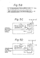
- Figures 5A ⁇ 5D, 6A ⁇ 6C, and 7A ⁇ 7B are block diagrams of the apparatus for carrying out the present invention, wherein Figs. 5A ⁇ 5D are block diagrams of a terminal transmitting portion; Figs. 6A ⁇ 6C are block diagrams of an intermediate repeater station; and Figs. 7A and 7B are block diagrams of a terminal receiving portion.
- Figs. 5A ⁇ 5D are block diagrams of a terminal transmitting portion
- Figs. 6A ⁇ 6C are block diagrams of an intermediate repeater station
- Figs. 7A and 7B are block diagrams of a terminal receiving portion.
- a synchronizing signal is added in a signal processing portion l4 to the system switching control signal input from an external source, and the system switching control signal is inserted into a specified channel, for example, the portion D1 of channel l in Fig. l.
- the order-wire signal and the low speed data signal input to the signal processing portion l5 are added to a frame synchronizing signal, further converted into parallel signals for two channels, and thereafter, inserted into portions D2 , D3 of CH3 , CH4 in Fig. l.
- the 4CH signals are then modulated as a carrier wave in a modulation portion 2, and a l6 value QAM modulation waveform is output to a next office.
- the order-wire signal and the low speed data signal are inserted via an inserting portion l2 ⁇ , l3 ⁇ into the same position in the frame format.
- Fig. 5A the main signals in CH1 and CH2 ⁇ CH4 are applied to the inserting portions l2 and l3 via a frequency converter (not shown in the drawing) in which gaps are provided in the main signal.
- reference numeral l6 denotes a signal applied to the inserting portion l2 or l3
- reference numeral l6a denotes a signal applied to the frequency converter mentioned above.
- FIG. 5C is a detailed block diagram of the signal processing portion l4, in which a sync. signal generator l4a generates a sync. signal F ⁇ , and the system switching control signal is combined with the sync. signal F ⁇ in a multiplexer l4b which is controlled by a controller l4C. The output of the multiplexer l4b is supplied to the gap corresponding to the portion D1.
- Figure 5D is a detailed block diagram of the signal processing portion l5.
- the function of the circuit shown in Fig. 5D is very similar to that of the circuit shown in Fig. 5C. That is, the order-wire signal and the low speed data signal are added the sync signal generated in a sync. signal generator l5a in a multiplexer l5b under the control of the controller l5c, and the output of the multiplexer l5b is supplied to the gap corresponding to the portions D2 , D3 in CH3 and CH4.
- Fig. 6A the l6 value QAM modulation waveform transmitted via the circuit is demodulated in demodulating portions 4, 4 ⁇ , and a signal having a format shown in Fig. l is taken out. Note, the CH1 signal is directly input to modulating portions 8, 8 ⁇ .
- the CH2 ⁇ 4 signals in the other channel l7 are applied to a selection/separation portion l8 in the signal processing means 2l and portions D2 or D3 having a good S/N ratio are selected, and thereafter, the signal is separated into the order-wire signal and the low speed data signal, to be output.
- the order-wire signal or the low speed data signal which were taken out or sent from the intermediate repeater station are added to the DSC synchronizing signal in the signal processing portion l9, as in the terminal office, and thereafter, inserted into portions D2 , D3 of the frame format shown in Fig. l in the inserting portion 20, 20 ⁇ , to be applied to the modulating portions 8, 8 ⁇ .
- the l6 value QAM modulation waveform is then repeated.
- FIG. 6B is a block diagram of one example of the selection/separation portion l8 in Fig. 6A.
- CH3 and CH4 input signals are supplied to a circuit l8a in which the frame sync. signals are extracted and the extracted sync. signal is supplied together with the input signals to latch circuits l8b and l8c and further supplied to the signal processing portion l9.
- the outputs of the latch circuits l8b and l8c are supplied to the F ⁇ frame sync.
- separating circuit l8d in which the frame signal F ⁇ is removed and supplied to an external circuit such as a telephone circuit or a data circuit.
- Figure 6C is a block diagram of one example of the signal processing circuit l9 shown in Fig. 6A.
- the external signals that is, the order-wire signal and the low speed data signals
- a multiplexer l9a with a sync. signal generated in a sync. generated l9b, under the control of the control circuit l9c controlled by the output of the circuit l8a, and supplied to the inserting portion 20.
- Fig. 7A the signal having a frame format shown in Fig. l demodulated in the demodulating portion 22, 22 ⁇ taken out, and the CH1 signal is supplied to a separation selection portion 23 so that a system switching control signal is taken out. Further, the CH2 ⁇ CH4 signals are added to the selection separation portion 24 so that the order-wire signal and the low speed data are taken out.
- the outputs, including the main signal, of separating circuits 25, 26, 25 ⁇ , 26 ⁇ are supplied respectively to a frequency converter (not shown in the drawings) and the insertion gaps are removed.
- reference numeral 30 denotes the output signal of the separating portion and reference signal 30a denotes the output of the frequency converter explained above.
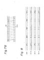
- Figure 8 is another example of a frame format of a digital multi-value quadrature amplitude modulation system in the case of the l6 value QAM system.
- "F” is a main signal frame synchronizing signal and "D1 ⁇ D3" are DSC signals, respectively.
- the difference between Fig. 8 and Fig. l is that the DSC signals are all inserted in the same channel, as shown in Fig. 8.
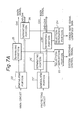
- Figures 9A ⁇ 9C are block diagrams of a conventional signal transmission system.
- a bipolar/unipolar converting (hereinafter called B/U conversion) portion 4l converts an input bipolar signal IN to a unipolar signal, inserted codes such as an error correcting code and a digital service channel (DSC) signal are processed in a transmitting code processing portion 42, multi-value quadrature modulation (hereinafter called multi-value QAM) is carried out in a modulating portion 43, and the output of the modulating portion 43 is transmitted from a transmitting portion 44.
- a DSC multiplexing portion 45 controls a switch 46, and multiplies a system control signal from the switch control portion 47 switching a main circuit and a protecting circuit and an order-wire signal used between specified stations so as to form one signal.
- a repeater station shown in Fig. 9B receives in a receiving portion 5l the signal from an upstream station, and in a modulating portion 52, demodulates the multi-value QAM signal into a two value digital signal and demodulates ASC signal which FM modulates a carrier wave.
- the repeater station branches and inserts a DSC signal, and in a modulating portion 54, the two value digital signal is modulated together with the ASC signal and sent to a transmitting portion 55.
- a DSC demultiplexing portion 56 demultiplexes and separates only the order signal between specified stations allocated to the station, among the multiplexed DSC signals.
- a receiving terminal station shown in Fig. 9C receives, in a receiving portion 6l, the digital signal and the ASC signal demodulated in a demodulating portion 62, a receiving signal processing portion 63, and code processes such as a separation of an error correction or DSC signal are carried out, and a U/B converting portion 64 carries out a U/B conversion, and outputs the result. Further, a DSC separating portion 65 separates the order signal between the specified stations and the system control signal, and a switch control portion 66 controls the switch 67 by the system control signal to switch the main circuit and the protecting circuit.
- the order-wire signal for all stations is used as ASC signal, and, the DSC signal, is formed by multiplying a plurality of order-wire signals between specified stations having different combinations of the stations to be used, and the system control signal used only between a transmitting terminal station and a receiving terminal station in which the system is switched.
- Figs. 9A ⁇ 9C DSC signals are branched and inserted in each station, and thus the reliability thereof is decreased at each station. Therefore, the reliability of the system control signal multiplied in the DSC signal is also decreased, so that a problem of a higher probability of an error occurring in the system control is increased.
- a first auxiliary signal which is required only in the transmitting station and the receiving station, such as used in the system control signal, and a second auxiliary signal required in the intermediate station are separate in different time slot, and in the intermediate station, only the second auxiliary signal is branched and inserted.
- the intermediate station does not branch or insert the first auxiliary signal, and thus the first auxiliary signal inserted in the time slot can be transmitted without any decrease in reliability.
- Figures l0A ⁇ l0B are block diagrams of an auxiliary signal transmission system of another embodiment of the present invention.
- a B/U conversion portion 7l, sending portions 74, 75, switches 76, 97, switch control portions 77, 96, and receiving portions 8l, 9l have the same function as shown in Figs. 9A ⁇ 9C, and therefore, the explanation thereof is omitted.
- a transmitting code processing portion 72 and a receiving code processing portion 93 a system control signal as a first auxiliary signal and a DSC signal as a second auxiliary signal are treated as different signals, and are inserted or branched by using different time slots.
- a DSC multiplexing portion 75, a DSC demultiplexing portion 86, and a DSC separating portion 95 instead of a system control signal, a digital order signal for all stations is multiplexed and demultiplexed with an order signal for a specified station.
- an ASC signal is not modulated and demodulated in modulating portions 73, 74 and demodulating portions 82, 83.
- the system control signal is not separated or inserted in the intermediate station shown in Fig. l0B, the reliability is not decreased. Further, instead of the system control signal, the order signal for all stations is multiplexed as a DSC signal, and therefore, it is not necessary to FM modulate the carrier wave due to the ASC signal, as in the prior art. Accordingly, a precise carrier wave regeneration can be carried out so that the receiving error rate is reduced.
- the auxiliary signal which is necessary in the transmitting station and the receiving station can be transmitted without decreasing the reliability of the operation, and the error probability in the system control decreased, and thus the reliability of the whole system is improved.
Landscapes
- Engineering & Computer Science (AREA)
- Computer Networks & Wireless Communication (AREA)
- Signal Processing (AREA)
- Physics & Mathematics (AREA)
- Electromagnetism (AREA)
- Time-Division Multiplex Systems (AREA)
Abstract
Description
- The present invention relates to an improvement of an auxiliary signal transmission system used, for example, in a digital microwave multiplex radio communication system.
- To carry out the transmission of a digitalized order signal, low speed data or a system switching control signal (generically known as the auxiliary signal) between the terminal office and the intermediate repeater station, between the intermediate stations, and between the terminal offices, by using the digital microwave multiplex radio system, the system is used for inserting these signals into a main signal (sometimes known as a digital service channel and hereinafter referred to as DSC), and in the intermediate repeater station, a signal processing is carried out in a signal processing portion, to take out or repeat the order-wire signal or the low speed data from the received signal. In this case, desirably the auxiliary signal transmission system prevents problems in the system even if a problem occurs in the intermediate repeater station.
- In a digital microwave multiplex radio system which transmits the auxiliary signal between the terminal office and the intermediate repeater station, or between intermediate repeater stations, if the transmission capacity is small, a system which performs a shallow frequency modulation of a carrier wave by this signal, to carry out an analogical transmission (such a system is known as an analog service channel) is used. However, for example, when the transmission capacity is large, such as in a digital multi-value quadrature amplitude modulation system, the purity of the regenerated carrier wave should be maintained at high degree, to ensure that any deterioration of an error rate of the main signal as kept as small as possible, and therefore, the above-mentioned service channel can not be used. Accordingly, a DSC system in which all digitalized signals, including the order signal, are included in the main signal and are transmitted, is used.
- There are four kinds of signals that can be transmitted by the DSC, i.e., the DSC synchronizing signal, the system switching control signal, the order-wire signal, and low speed data. The order-wire signal and low speed data are necessary in both the intermediate repeater station and the terminal office, but the system switching control signal is necessary only in the terminal office.
- The system switching control signal is used for to prevent problems in the main circuit and to maintain the quality of the main signal, and is the most important among the signals transmitted by the DSC.
- On the other hand, in the signal processing portion in the intermediate repeater station, as mentioned already, the order-wire signal and the low speed data are taken out only after all of the other DSC signals are taken out. Therefore, if a fault occurs in this portion, a problem arises in that the system switching control signal can not be repeated to the receiving terminal office, and thus problems arise in the operation of the main circuit.
- An object of the present invention is to provide an auxiliary signal transmission system to be used in the multiplex communication system which can prevent problems in the system even if a problem arises in the intermediate repeater station.
- The above-mentioned object is achieved by providing an auxiliary signal transmission system to be used in a multiplex communication system which includes a transmitting terminal, one or a plurality of intermediate repeater stations, and a receiving terminal, wherein the multiplex communication system communicates, together with main signal, a first kind of auxiliary signal such as a system switching control signal which is necessary only in the transmitting terminal and the receiving terminal and a second kind of auxiliary signal such as an order-wire signal, and low speed data which is necessary at least one intermediate repeater station. The multiplex communication system is formed by a plurality of channels, each of which is formed by a plurality of time slots, for transmitting the auxiliary signals together with main signals and comprises a means for inserting the first kind of auxiliary signal separately from the second kind of the auxiliary signal in the main signal in the transmitting terminal; a means for transmitting the first kind of auxiliary signal without processing the second kind of auxiliary signal in the intermediate repeater station, and a means for processing the second kind of auxiliary signal in the intermediate repeater station, and after processing the first kind of auxiliary signal, transmitting the second kind of auxiliary signal from the intermediate repeater station to the receiving terminal or the next intermediate repeater station.
- Further features and advantages of the present invention will be apparent from the ensuing description with reference to the accompanying drawings to which, however, the scope of the invention is in no way limited.
-
- Figure l is a diagram showing a format used in a digital multiplex modulation system;
- Fig. 2 is a diagram showing a construction of a conventional system;
- Figs. 3A, 3B, and 3C are block diagrams showing the operation of the conventional system;
- Fig. 4 is a block diagram showing the principle of the system according to the present invention;
- Figs. 5A to 5D are diagrams showing one embodiment of a transmitting terminal of the present invention;
- Figs. 6A to 6C are diagrams showing one embodiment of an intermediate repeater station of the present invention;
- Figs. 7A and 7B are diagrams showing one embodiment of a receiving terminal of the present invention;
- Fig. 8 is a diagram showing a format of another embodiment of the present invention;
- Figs. 9A - 9C are diagrams showing examples of the conventional system; and,
- Figs. l0A - l0C are diagrams showing another embodiment of the system according to the present invention.
- Figure l shows an example of a frame format of a digital multi-value quadrature amplitude modulation system having l6 values (hereinafter referred to as l6 value QAM modulation system).
- In Fig. l, F₁₁ ∿ F1n , F₂₁ ∿ F2n , F₃₁ ∿ F3n , F₄₁ ∿ F4n show main signal frame synchronizing signals, "M" shows a main signal sequence, "C" shows a stuff control signal, "P" shows a parity bit, and "D₁ ∿ D₃" show a DSC signal, respectively.
- In Fig. l, the DSC signal or the stuff control signal or the parity bit and main signal sequences are inserted between the main signal frame synchronizing signals, which are repeated at a constant period. Note, in a 64 value QAM modulation system, 6 channels are used (hereinafter abbreviated as CH), and in a 256 value QAM modulation system 8CH are used.
- Figure 2 is a diagram showing an example of a construction of a conventional circuit.
- As shown in Fig. 2, when a terminal office transmitting portion and a terminal office receiving portion are provided at two ends and an intermediate repeater station is provided therebetween, the intermediate repeater portion extracts all of the DSC signals D₁ ∿ D₃ , in order to take out the order-wire signal and the low speed data included in the D₁ ∿ D₃ portion in the example of the frame format of Fig. l, the order-wire signal and the low speed data signal are separated therefrom and these signals are again inserted to the main signal, as a repeat of the procedure.
- Figs. 3A ∿ 3C are block diagrams of an apparatus for carrying out the operation of the conventional system; wherein Fig. 3A shows a terminal office transmitting portion, Fig. 3B an intermediate repeater station, and Fig. 3C a terminal office receiving portion. Hereinafter, the operation of the conventional system will be explained, with reference to Figs. 3A ∿ 3C and on the assumption that the system has 4 channels.
- In Fig. 3A, a main signal whose transmission speed has been accelerated at a velocity converting portion (not shown in the drawing) and gaps provided therein, is input to a main circuit. Further, a frame synchronizing signal is added to a system switching control signal, an order-wire signal, and low speed data in a
signal processing portion 3, converted into three parallel signals, output along three channels, and thereafter, inserted into the gaps in the main signal at an inserting portion l, so to obtain a 4CH signal having the format shown in Fig. l. This signal is supplied to a modulatingportion 2, wherein the carrier wave is modulated, and the modulated waveform as a l6 value QAM is sent to a next office. - A protecting circuit is also processed in the same way as the main circuit mentioned above, and the l6 value QAM modulated waveform is sent via an inserting portion lʹ and a modulating portion 2ʹ to the next office. Note, in this case a protecting circuit test signal is used instead of the main signal.
- In Fig. 3B, the l6 value QAM modulated waveform applied to demodulating
portions 4, 4ʹ via a main circuit and a protecting circuit is demodulated and a signal having a format shown in Fig. l is obtained and applied to a selecting and separatingportion 5, so that the D₁ ∿ D₃ portions of transmitted by the main circuit and the protecting circuit are taken out and an order-wire signal and low speed data signal having a good S/N ratio are obtained. - Then, the taken out order signal and low speed data are processed together with the system switching signal in the
signal processing portion 6, in the same way as mentioned above, and are inserted in the insertingportion 7 and 7ʹ into the portions D₁ ∿ D₃ shown in Fig. l. Thereafter, the carrier wave is modulated in the modulatingportions 8 and 8ʹ, and the l6 value QAM modulated waveform is sent to a next office. - In Fig. 3C, the l6 value QAM modulated waveform from the intermediate repeater station is demodulated in the demodulating
portions 9 and 9ʹ, to obtain a signal having the format shown in Fig. l. This signal is separated in the separating portions l0 and l0ʹ into the main signal, the protecting circuit test signal, and the portions D₁ ∿ D₃ , and thereafter, as in Fig. 3B, the portions D₁ ∿ D₃ having a good S/N ratio are selected in a selecting and separating portion ll, and the system switching control signal, the order-wire signal, and the low speed data signal are obtained therefrom. - In the example as shown above, the signal transmitted by using the DSC is formed by 4 kinds of signals, i.e., the DSC synchronizing signal, the system switching control signal, the order-wire signal, and the low speed data signal. The order-wire signal and the low speed data signal are necessary in both the intermediate repeater station and the terminal offices, but the system switching control signal is necessary only in the terminal offices.
- The system switching control signal is used to prevent problems in the main circuit, and to maintain the quality of the main signal, and is the most important among the signals transmitted by the DSC.
- In the signal processing portion in the intermediate repeater station, as mentioned above, the order-wire signal and the low speed data signal are taken out only after all of the DSC signals are taken out. Therefore, if a fault occurs in this portion, a problem arises in that the system switching control signal can not be repeated to the terminal office, and therefore, problems in the main circuit can not be prevented.
- The above-mentioned problem can be solved by providing an auxiliary signal transmission system in which, as shown in Fig. 4, in the transmitting portion, a digital service channel synchronizing signal is added to the system switching control signal in a signal processing portion l4, and to the order-wire signal and the low speed data in a signal processing portion l5, respectively, and thereafter, is inserted via inserting portion l2, l3 into a main signal having a specified channel (CH₁) l6 or another channel (CH₃ , CH₄) l7, to be output, and in an intermediate repeater station, the signal of the specified channel (CH₁) l6 is directly repeated without signal processing, and the order-wire signal and the low speed data signal in the other channel (CH₃ , CH₄) l7 are taken out by signal processing in a signal processing means 2l, or after a repeated signal process processing, are inserted via the inserting
portion 20 into the main signal of the other (CH₃ , CH₄) channel l7, to be repeated. - As shown in Fig. 4 of the present invention, a DSC synchronizing signal and a system switching control signal are inserted via an inserting portion l2 into a main signal of a specified channel l6, and the DSC synchronizing signal, and an order-wire signal and a low speed data signal are inserted via an inserting portion l3 into a main signal of another (CH₃ , CH₄) channel l7. In the intermediate repeater station, the signal of the specified channel l6 is repeated without processing, and only the order-wire signal and the low speed data signal of the other (CH₃ , CH₄) channel l7 are processed and taken out in a signal processing means 2l, or again processed and inserted via an inserting
portion 20 into this channel l7, to be repeated. - That is, since the system switching control signal is not processed in the intermediate repeater station, if an obstacle arises in the signal processing portion, the system switching control signal is transmitted to a terminal receiving portion, and thus the occurrence of a fault in the system can be prevented.
- Figures 5A ∿ 5D, 6A ∿ 6C, and 7A ∿ 7B are block diagrams of the apparatus for carrying out the present invention, wherein Figs. 5A ∿ 5D are block diagrams of a terminal transmitting portion; Figs. 6A ∿ 6C are block diagrams of an intermediate repeater station; and Figs. 7A and 7B are block diagrams of a terminal receiving portion. Note, throughout the drawings the same symbols designate the same elements. Hereinafter, assuming that the number n of the channels is 4, the operation of Figs. 5A ∿ 5D, 6A ∿ 6C, and 7A, 7B will be explained with reference also to Fig. l.
- In Fig. 5A, a synchronizing signal is added in a signal processing portion l4 to the system switching control signal input from an external source, and the system switching control signal is inserted into a specified channel, for example, the portion D₁ of channel l in Fig. l.
- Further, the order-wire signal and the low speed data signal input to the signal processing portion l5 are added to a frame synchronizing signal, further converted into parallel signals for two channels, and thereafter, inserted into portions D₂ , D₃ of CH₃ , CH₄ in Fig. l. The 4CH signals are then modulated as a carrier wave in a
modulation portion 2, and a l6 value QAM modulation waveform is output to a next office. Similarly, in a protecting circuit, the order-wire signal and the low speed data signal are inserted via an inserting portion l2ʹ, l3ʹ into the same position in the frame format. - In Fig. 5A, the main signals in CH₁ and CH₂ ∿ CH₄ are applied to the inserting portions l2 and l3 via a frequency converter (not shown in the drawing) in which gaps are provided in the main signal. In Fig. 5B, reference numeral l6 denotes a signal applied to the inserting portion l2 or l3, and reference numeral l6a denotes a signal applied to the frequency converter mentioned above.
- Figure 5C is a detailed block diagram of the signal processing portion l4, in which a sync. signal generator l4a generates a sync. signal Fʹ, and the system switching control signal is combined with the sync. signal Fʹ in a multiplexer l4b which is controlled by a controller l4C. The output of the multiplexer l4b is supplied to the gap corresponding to the portion D₁.
- Figure 5D is a detailed block diagram of the signal processing portion l5. The function of the circuit shown in Fig. 5D is very similar to that of the circuit shown in Fig. 5C. That is, the order-wire signal and the low speed data signal are added the sync signal generated in a sync. signal generator l5a in a multiplexer l5b under the control of the controller l5c, and the output of the multiplexer l5b is supplied to the gap corresponding to the portions D₂ , D₃ in CH₃ and CH₄.
- Next, in Fig. 6A, the l6 value QAM modulation waveform transmitted via the circuit is demodulated in
demodulating portions 4, 4ʹ, and a signal having a format shown in Fig. l is taken out. Note, the CH₁ signal is directly input to modulatingportions 8, 8ʹ. - The CH₂ ∿ ₄ signals in the other channel l7 are applied to a selection/separation portion l8 in the signal processing means 2l and portions D₂ or D₃ having a good S/N ratio are selected, and thereafter, the signal is separated into the order-wire signal and the low speed data signal, to be output.
- Further, the order-wire signal or the low speed data signal which were taken out or sent from the intermediate repeater station, are added to the DSC synchronizing signal in the signal processing portion l9, as in the terminal office, and thereafter, inserted into portions D₂ , D₃ of the frame format shown in Fig. l in the inserting
portion 20, 20ʹ, to be applied to the modulatingportions 8, 8ʹ. The l6 value QAM modulation waveform is then repeated. - Figure 6B is a block diagram of one example of the selection/separation portion l8 in Fig. 6A. In Fig. 6B, CH₃ and CH₄ input signals are supplied to a circuit l8a in which the frame sync. signals are extracted and the extracted sync. signal is supplied together with the input signals to latch circuits l8b and l8c and further supplied to the signal processing portion l9. The outputs of the latch circuits l8b and l8c are supplied to the Fʹ frame sync. separating circuit l8d, in which the frame signal Fʹ is removed and supplied to an external circuit such as a telephone circuit or a data circuit.
- Figure 6C is a block diagram of one example of the signal processing circuit l9 shown in Fig. 6A. As shown in Fig. 6C, the external signals, that is, the order-wire signal and the low speed data signals, are multiplexed in a multiplexer l9a with a sync. signal generated in a sync. generated l9b, under the control of the control circuit l9c controlled by the output of the circuit l8a, and supplied to the inserting
portion 20. - Next, in Fig. 7A, the signal having a frame format shown in Fig. l demodulated in the
demodulating portion 22, 22ʹ taken out, and the CH₁ signal is supplied to a separation selection portion 23 so that a system switching control signal is taken out. Further, the CH₂ ∿ CH₄ signals are added to theselection separation portion 24 so that the order-wire signal and the low speed data are taken out. The outputs, including the main signal, of separatingcircuits reference numeral 30 denotes the output signal of the separating portion andreference signal 30a denotes the output of the frequency converter explained above. - By performing the signal processing shown in Fig. 5A to Fig. 7B, if a fault occurs in the signal processing means 2l of the intermediate repeater station, problems in the system can be prevented without affect on the switching control signal.
- Figure 8 is another example of a frame format of a digital multi-value quadrature amplitude modulation system in the case of the l6 value QAM system. In Fig. 8, "F" is a main signal frame synchronizing signal and "D₁ ∿ D₃" are DSC signals, respectively. The difference between Fig. 8 and Fig. l is that the DSC signals are all inserted in the same channel, as shown in Fig. 8.
- The system using the format shown in Fig. 8 was conventionally performed as shown in Figs. 9A ∿ 9C.
- Figures 9A ∿ 9C are block diagrams of a conventional signal transmission system.
- In transmitting station shown in Fig. 9A, a bipolar/unipolar converting (hereinafter called B/U conversion) portion 4l converts an input bipolar signal IN to a unipolar signal, inserted codes such as an error correcting code and a digital service channel (DSC) signal are processed in a transmitting
code processing portion 42, multi-value quadrature modulation (hereinafter called multi-value QAM) is carried out in a modulatingportion 43, and the output of the modulatingportion 43 is transmitted from a transmittingportion 44. Further, aDSC multiplexing portion 45 controls aswitch 46, and multiplies a system control signal from theswitch control portion 47 switching a main circuit and a protecting circuit and an order-wire signal used between specified stations so as to form one signal. - A repeater station shown in Fig. 9B receives in a receiving portion 5l the signal from an upstream station, and in a modulating
portion 52, demodulates the multi-value QAM signal into a two value digital signal and demodulates ASC signal which FM modulates a carrier wave. Next, in an SCsignal processing portion 53, the repeater station branches and inserts a DSC signal, and in a modulatingportion 54, the two value digital signal is modulated together with the ASC signal and sent to a transmittingportion 55. Further, aDSC demultiplexing portion 56 demultiplexes and separates only the order signal between specified stations allocated to the station, among the multiplexed DSC signals. - A receiving terminal station shown in Fig. 9C receives, in a receiving portion 6l, the digital signal and the ASC signal demodulated in a
demodulating portion 62, a receivingsignal processing portion 63, and code processes such as a separation of an error correction or DSC signal are carried out, and a U/B converting portion 64 carries out a U/B conversion, and outputs the result. Further, aDSC separating portion 65 separates the order signal between the specified stations and the system control signal, and aswitch control portion 66 controls theswitch 67 by the system control signal to switch the main circuit and the protecting circuit. - Here, the order-wire signal for all stations is used as ASC signal, and, the DSC signal, is formed by multiplying a plurality of order-wire signals between specified stations having different combinations of the stations to be used, and the system control signal used only between a transmitting terminal station and a receiving terminal station in which the system is switched.
- In Figs. 9A ∿ 9C, DSC signals are branched and inserted in each station, and thus the reliability thereof is decreased at each station. Therefore, the reliability of the system control signal multiplied in the DSC signal is also decreased, so that a problem of a higher probability of an error occurring in the system control is increased.
- To solve the above-mentioned problem, in the present invention, a first auxiliary signal which is required only in the transmitting station and the receiving station, such as used in the system control signal, and a second auxiliary signal required in the intermediate station, are separate in different time slot, and in the intermediate station, only the second auxiliary signal is branched and inserted.
- That is, the intermediate station does not branch or insert the first auxiliary signal, and thus the first auxiliary signal inserted in the time slot can be transmitted without any decrease in reliability.
- Figures l0A ∿ l0B are block diagrams of an auxiliary signal transmission system of another embodiment of the present invention.
- In Figs. l0A ∿ l0C, a B/U conversion portion 7l, sending
portions switch control portions 77, 96, and receiving portions 8l, 9l have the same function as shown in Figs. 9A ∿ 9C, and therefore, the explanation thereof is omitted. - The difference between Figs. 9A ∿ 9C and Figs. l0A ∿ l0C lies in the following. In a transmitting
code processing portion 72 and a receivingcode processing portion 93, a system control signal as a first auxiliary signal and a DSC signal as a second auxiliary signal are treated as different signals, and are inserted or branched by using different time slots. In aDSC multiplexing portion 75, aDSC demultiplexing portion 86, and aDSC separating portion 95, instead of a system control signal, a digital order signal for all stations is multiplexed and demultiplexed with an order signal for a specified station. Further, an ASC signal is not modulated and demodulated in modulatingportions demodulating portions - Because, the system control signal is not separated or inserted in the intermediate station shown in Fig. l0B, the reliability is not decreased. Further, instead of the system control signal, the order signal for all stations is multiplexed as a DSC signal, and therefore, it is not necessary to FM modulate the carrier wave due to the ASC signal, as in the prior art. Accordingly, a precise carrier wave regeneration can be carried out so that the receiving error rate is reduced.
- As mentioned above, according to the present invention, the auxiliary signal which is necessary in the transmitting station and the receiving station can be transmitted without decreasing the reliability of the operation, and the error probability in the system control decreased, and thus the reliability of the whole system is improved.
Claims (4)
means for inserting said first auxiliary signal separately from said second auxiliary signal in said main signal in said transmitting terminal;
means for transmitting said first auxiliary signal without processing said first auxiliary signal in said intermediate repeater station, and
means for processing said auxiliary signal in said intermediate repeater station, and after processing said second auxiliary signal, transmitting said second auxiliary signal from said intermediate repeater station to said receiving terminal or next intermediate repeater station.
Applications Claiming Priority (4)
| Application Number | Priority Date | Filing Date | Title |
|---|---|---|---|
| JP115362/86 | 1986-05-19 | ||
| JP11536286A JPS62269521A (en) | 1986-05-19 | 1986-05-19 | Auxiliary signal transmission system |
| JP122013/86 | 1986-05-27 | ||
| JP12201386A JPS62278830A (en) | 1986-05-27 | 1986-05-27 | Sub-signal transmitting system |
Publications (3)
| Publication Number | Publication Date |
|---|---|
| EP0246619A2 true EP0246619A2 (en) | 1987-11-25 |
| EP0246619A3 EP0246619A3 (en) | 1990-04-18 |
| EP0246619B1 EP0246619B1 (en) | 1993-11-03 |
Family
ID=26453886
Family Applications (1)
| Application Number | Title | Priority Date | Filing Date |
|---|---|---|---|
| EP87107279A Expired - Lifetime EP0246619B1 (en) | 1986-05-19 | 1987-05-19 | System and method for transmitting auxiliary signal in a multiplex communication system |
Country Status (4)
| Country | Link |
|---|---|
| US (1) | US4860282A (en) |
| EP (1) | EP0246619B1 (en) |
| CA (1) | CA1275515C (en) |
| DE (1) | DE3787997T2 (en) |
Cited By (5)
| Publication number | Priority date | Publication date | Assignee | Title |
|---|---|---|---|---|
| EP0359261A3 (en) * | 1988-09-14 | 1991-10-09 | Fujitsu Limited | Subsignal transmitting system |
| EP0635988A1 (en) * | 1993-07-23 | 1995-01-25 | Ericsson GE Mobile Communications Inc. | Narrow band simulcast system having low speed data distribution |
| US6011977A (en) * | 1995-11-30 | 2000-01-04 | Ericsson Inc. | RF simulcasting system with dynamic wide-range automatic synchronization |
| US6490272B1 (en) | 1992-11-30 | 2002-12-03 | Telefonaktiebolaget Lm Ericsson | Radio link network and a method for transferring additional services in a radio link network |
| CN113219941A (en) * | 2021-04-22 | 2021-08-06 | 湖南联塑科技实业有限公司 | Signal linking and confirming method between industrial equipment |
Families Citing this family (3)
| Publication number | Priority date | Publication date | Assignee | Title |
|---|---|---|---|---|
| JP2564375B2 (en) * | 1988-09-28 | 1996-12-18 | 株式会社日立製作所 | Drop-and-drop multiplexer |
| US5768295A (en) * | 1995-03-10 | 1998-06-16 | Nec Corporation | System for parity calculation based on arithemtic difference between data |
| CA2317708A1 (en) * | 1998-11-02 | 2000-05-11 | Koninklijke Philips Electronics N.V. | Communication system using a multiplex signal carrying an auxiliary signal |
Citations (1)
| Publication number | Priority date | Publication date | Assignee | Title |
|---|---|---|---|---|
| GB2145608A (en) | 1983-08-22 | 1985-03-27 | Gen Electric Plc | Multiplex transmission systems |
Family Cites Families (6)
| Publication number | Priority date | Publication date | Assignee | Title |
|---|---|---|---|---|
| US3939407A (en) * | 1973-12-03 | 1976-02-17 | Raytheon Company | Plural channel communications system |
| US4434485A (en) * | 1980-11-13 | 1984-02-28 | Rockwell International Corporation | Drop and insert channel bank with reduced channel units |
| JPS58134545A (en) * | 1982-02-04 | 1983-08-10 | Nec Corp | Service channel signal transmitting system |
| GB2132455A (en) * | 1982-12-08 | 1984-07-04 | Racal Res Ltd | Communications systems |
| JPS60107936A (en) * | 1983-11-16 | 1985-06-13 | Fujitsu Ltd | Auxiliary signal inserting circuit |
| US4667319A (en) * | 1985-07-29 | 1987-05-19 | Gte Sprint Communications Corporation | Digital repeater with 3-way branching of service channels |
-
1987
- 1987-05-12 CA CA000536920A patent/CA1275515C/en not_active Expired - Lifetime
- 1987-05-19 DE DE87107279T patent/DE3787997T2/en not_active Expired - Fee Related
- 1987-05-19 EP EP87107279A patent/EP0246619B1/en not_active Expired - Lifetime
-
1988
- 1988-12-22 US US07/289,436 patent/US4860282A/en not_active Expired - Fee Related
Patent Citations (1)
| Publication number | Priority date | Publication date | Assignee | Title |
|---|---|---|---|---|
| GB2145608A (en) | 1983-08-22 | 1985-03-27 | Gen Electric Plc | Multiplex transmission systems |
Cited By (5)
| Publication number | Priority date | Publication date | Assignee | Title |
|---|---|---|---|---|
| EP0359261A3 (en) * | 1988-09-14 | 1991-10-09 | Fujitsu Limited | Subsignal transmitting system |
| US6490272B1 (en) | 1992-11-30 | 2002-12-03 | Telefonaktiebolaget Lm Ericsson | Radio link network and a method for transferring additional services in a radio link network |
| EP0635988A1 (en) * | 1993-07-23 | 1995-01-25 | Ericsson GE Mobile Communications Inc. | Narrow band simulcast system having low speed data distribution |
| US6011977A (en) * | 1995-11-30 | 2000-01-04 | Ericsson Inc. | RF simulcasting system with dynamic wide-range automatic synchronization |
| CN113219941A (en) * | 2021-04-22 | 2021-08-06 | 湖南联塑科技实业有限公司 | Signal linking and confirming method between industrial equipment |
Also Published As
| Publication number | Publication date |
|---|---|
| DE3787997D1 (en) | 1993-12-09 |
| US4860282A (en) | 1989-08-22 |
| EP0246619B1 (en) | 1993-11-03 |
| CA1275515C (en) | 1990-10-23 |
| EP0246619A3 (en) | 1990-04-18 |
| DE3787997T2 (en) | 1994-04-21 |
Similar Documents
| Publication | Publication Date | Title |
|---|---|---|
| US5499241A (en) | Broadband communications system | |
| CA1229436A (en) | Multidirection multiplex communication systems | |
| EP0246619A2 (en) | System and method for transmitting auxiliary signal in a multiplex communication system | |
| US5483370A (en) | Crossconnect apparatus for a coherent transmission system | |
| CA1306011C (en) | Transponder frequency offset compensation with recurrently assigned unique words | |
| EP0327101A2 (en) | Satellite communication system with variable coding rate | |
| EP0359261B1 (en) | Subsignal transmitting system | |
| CA1281144C (en) | Multiplexing apparatus having bsi-code processing and bit interleave functions | |
| JP2001053705A (en) | Transmission equipment | |
| US2225741A (en) | Television and other signal transmission systems | |
| US4719623A (en) | Method of receiving time multiplexed signals together with energy requirements of receiver over a multiplex signal transmission path | |
| JPH104391A (en) | Multi-carrier transmission method | |
| EP1191726A1 (en) | A method of transmitting data symbols in a digital teletransmission network; a digital teletransmission network and network elements therefor | |
| JP3740537B2 (en) | Clock synchronization signal transmission system, data transmission system, and methods thereof | |
| JP3190835B2 (en) | Data communication device and method | |
| JPS6231229A (en) | Repeater | |
| EP0092957A2 (en) | Communication system | |
| KR100522123B1 (en) | Channel DeMUX Apparatus and Method in a Gap Filler System | |
| JPS6345932A (en) | Transmission circuit for digital service channel signal | |
| KR920005905B1 (en) | Transponder frquency offset compensation with recurrently assigned unique words | |
| JPS6388923A (en) | Frequency division multiple access communication equipment | |
| JP2671803B2 (en) | Data multiplex transmission device | |
| JPH06318924A (en) | Wireless communication system | |
| JP2541121B2 (en) | DS3 frame transceiver | |
| Buff | Twinplex and Twinmode Radiotelegraph Systems |
Legal Events
| Date | Code | Title | Description |
|---|---|---|---|
| PUAI | Public reference made under article 153(3) epc to a published international application that has entered the european phase |
Free format text: ORIGINAL CODE: 0009012 |
|
| AK | Designated contracting states |
Kind code of ref document: A2 Designated state(s): DE FR GB IT |
|
| PUAL | Search report despatched |
Free format text: ORIGINAL CODE: 0009013 |
|
| AK | Designated contracting states |
Kind code of ref document: A3 Designated state(s): DE FR GB IT |
|
| 17P | Request for examination filed |
Effective date: 19900525 |
|
| 17Q | First examination report despatched |
Effective date: 19920327 |
|
| ITF | It: translation for a ep patent filed | ||
| GRAA | (expected) grant |
Free format text: ORIGINAL CODE: 0009210 |
|
| AK | Designated contracting states |
Kind code of ref document: B1 Designated state(s): DE FR GB IT |
|
| REF | Corresponds to: |
Ref document number: 3787997 Country of ref document: DE Date of ref document: 19931209 |
|
| ET | Fr: translation filed | ||
| PLBI | Opposition filed |
Free format text: ORIGINAL CODE: 0009260 |
|
| 26 | Opposition filed |
Opponent name: ALCATEL N.V. Effective date: 19940803 |
|
| PLBO | Opposition rejected |
Free format text: ORIGINAL CODE: EPIDOS REJO |
|
| PLBN | Opposition rejected |
Free format text: ORIGINAL CODE: 0009273 |
|
| STAA | Information on the status of an ep patent application or granted ep patent |
Free format text: STATUS: OPPOSITION REJECTED |
|
| 27O | Opposition rejected |
Effective date: 19970116 |
|
| PGFP | Annual fee paid to national office [announced via postgrant information from national office to epo] |
Ref country code: GB Payment date: 19980511 Year of fee payment: 12 Ref country code: FR Payment date: 19980511 Year of fee payment: 12 |
|
| PGFP | Annual fee paid to national office [announced via postgrant information from national office to epo] |
Ref country code: DE Payment date: 19980522 Year of fee payment: 12 |
|
| PG25 | Lapsed in a contracting state [announced via postgrant information from national office to epo] |
Ref country code: GB Free format text: LAPSE BECAUSE OF NON-PAYMENT OF DUE FEES Effective date: 19990519 |
|
| GBPC | Gb: european patent ceased through non-payment of renewal fee |
Effective date: 19990519 |
|
| PG25 | Lapsed in a contracting state [announced via postgrant information from national office to epo] |
Ref country code: FR Free format text: LAPSE BECAUSE OF NON-PAYMENT OF DUE FEES Effective date: 20000131 |
|
| PG25 | Lapsed in a contracting state [announced via postgrant information from national office to epo] |
Ref country code: DE Free format text: LAPSE BECAUSE OF NON-PAYMENT OF DUE FEES Effective date: 20000301 |
|
| REG | Reference to a national code |
Ref country code: FR Ref legal event code: ST |
|
| PG25 | Lapsed in a contracting state [announced via postgrant information from national office to epo] |
Ref country code: IT Free format text: LAPSE BECAUSE OF NON-PAYMENT OF DUE FEES;WARNING: LAPSES OF ITALIAN PATENTS WITH EFFECTIVE DATE BEFORE 2007 MAY HAVE OCCURRED AT ANY TIME BEFORE 2007. THE CORRECT EFFECTIVE DATE MAY BE DIFFERENT FROM THE ONE RECORDED. Effective date: 20050519 |