EP0243953A2 - Compound semiconductor device - Google Patents
Compound semiconductor device Download PDFInfo
- Publication number
- EP0243953A2 EP0243953A2 EP87106250A EP87106250A EP0243953A2 EP 0243953 A2 EP0243953 A2 EP 0243953A2 EP 87106250 A EP87106250 A EP 87106250A EP 87106250 A EP87106250 A EP 87106250A EP 0243953 A2 EP0243953 A2 EP 0243953A2
- Authority
- EP
- European Patent Office
- Prior art keywords
- compound semiconductor
- film layers
- semiconductor thin
- electric field
- thin
- Prior art date
- Legal status (The legal status is an assumption and is not a legal conclusion. Google has not performed a legal analysis and makes no representation as to the accuracy of the status listed.)
- Granted
Links
Images


Classifications
-
- H—ELECTRICITY
- H10—SEMICONDUCTOR DEVICES; ELECTRIC SOLID-STATE DEVICES NOT OTHERWISE PROVIDED FOR
- H10D—INORGANIC ELECTRIC SEMICONDUCTOR DEVICES
- H10D30/00—Field-effect transistors [FET]
- H10D30/40—FETs having zero-dimensional [0D], one-dimensional [1D] or two-dimensional [2D] charge carrier gas channels
- H10D30/47—FETs having zero-dimensional [0D], one-dimensional [1D] or two-dimensional [2D] charge carrier gas channels having two-dimensional [2D] charge carrier gas channels, e.g. nanoribbon FETs or high electron mobility transistors [HEMT]
- H10D30/471—High electron mobility transistors [HEMT] or high hole mobility transistors [HHMT]
- H10D30/473—High electron mobility transistors [HEMT] or high hole mobility transistors [HHMT] having confinement of carriers by multiple heterojunctions, e.g. quantum well HEMT
- H10D30/4732—High electron mobility transistors [HEMT] or high hole mobility transistors [HHMT] having confinement of carriers by multiple heterojunctions, e.g. quantum well HEMT using Group III-V semiconductor material
-
- H—ELECTRICITY
- H10—SEMICONDUCTOR DEVICES; ELECTRIC SOLID-STATE DEVICES NOT OTHERWISE PROVIDED FOR
- H10D—INORGANIC ELECTRIC SEMICONDUCTOR DEVICES
- H10D62/00—Semiconductor bodies, or regions thereof, of devices having potential barriers
- H10D62/80—Semiconductor bodies, or regions thereof, of devices having potential barriers characterised by the materials
- H10D62/81—Semiconductor bodies, or regions thereof, of devices having potential barriers characterised by the materials of structures exhibiting quantum-confinement effects, e.g. single quantum wells; of structures having periodic or quasi-periodic potential variation
- H10D62/815—Semiconductor bodies, or regions thereof, of devices having potential barriers characterised by the materials of structures exhibiting quantum-confinement effects, e.g. single quantum wells; of structures having periodic or quasi-periodic potential variation of structures having periodic or quasi-periodic potential variation, e.g. superlattices or multiple quantum wells [MQW]
- H10D62/8161—Semiconductor bodies, or regions thereof, of devices having potential barriers characterised by the materials of structures exhibiting quantum-confinement effects, e.g. single quantum wells; of structures having periodic or quasi-periodic potential variation of structures having periodic or quasi-periodic potential variation, e.g. superlattices or multiple quantum wells [MQW] potential variation due to variations in composition or crystallinity, e.g. heterojunction superlattices
- H10D62/8162—Semiconductor bodies, or regions thereof, of devices having potential barriers characterised by the materials of structures exhibiting quantum-confinement effects, e.g. single quantum wells; of structures having periodic or quasi-periodic potential variation of structures having periodic or quasi-periodic potential variation, e.g. superlattices or multiple quantum wells [MQW] potential variation due to variations in composition or crystallinity, e.g. heterojunction superlattices having quantum effects only in the vertical direction, i.e. layered structures having quantum effects solely resulting from vertical potential variation
- H10D62/8164—Semiconductor bodies, or regions thereof, of devices having potential barriers characterised by the materials of structures exhibiting quantum-confinement effects, e.g. single quantum wells; of structures having periodic or quasi-periodic potential variation of structures having periodic or quasi-periodic potential variation, e.g. superlattices or multiple quantum wells [MQW] potential variation due to variations in composition or crystallinity, e.g. heterojunction superlattices having quantum effects only in the vertical direction, i.e. layered structures having quantum effects solely resulting from vertical potential variation comprising only semiconductor materials
-
- H—ELECTRICITY
- H10—SEMICONDUCTOR DEVICES; ELECTRIC SOLID-STATE DEVICES NOT OTHERWISE PROVIDED FOR
- H10D—INORGANIC ELECTRIC SEMICONDUCTOR DEVICES
- H10D64/00—Electrodes of devices having potential barriers
- H10D64/01—Manufacture or treatment
- H10D64/011—Manufacture or treatment of electrodes ohmically coupled to a semiconductor
- H10D64/0116—Manufacture or treatment of electrodes ohmically coupled to a semiconductor to Group III-V semiconductors
-
- H—ELECTRICITY
- H10—SEMICONDUCTOR DEVICES; ELECTRIC SOLID-STATE DEVICES NOT OTHERWISE PROVIDED FOR
- H10D—INORGANIC ELECTRIC SEMICONDUCTOR DEVICES
- H10D64/00—Electrodes of devices having potential barriers
- H10D64/60—Electrodes characterised by their materials
- H10D64/62—Electrodes ohmically coupled to a semiconductor
-
- H—ELECTRICITY
- H10—SEMICONDUCTOR DEVICES; ELECTRIC SOLID-STATE DEVICES NOT OTHERWISE PROVIDED FOR
- H10D—INORGANIC ELECTRIC SEMICONDUCTOR DEVICES
- H10D62/00—Semiconductor bodies, or regions thereof, of devices having potential barriers
- H10D62/80—Semiconductor bodies, or regions thereof, of devices having potential barriers characterised by the materials
- H10D62/85—Semiconductor bodies, or regions thereof, of devices having potential barriers characterised by the materials being Group III-V materials, e.g. GaAs
Definitions
- the present invention relates to a compound semiconductor device, more particularly, to a compound semiconductor device specially suited for manufacturing component device of integrated circuits (IC) and large-scale integrated circuits (LSI) among those compound semiconductor devices such as field effect transistors (FET), high electron movement transistors (HEMT) and the like.
- IC integrated circuits
- LSI large-scale integrated circuits
- FET field effect transistors
- HEMT high electron movement transistors
- the epitaxial growth method is generally employed owing to the thin and uniform growth of layer and ease of control of constituent element composition ratio.
- the molecular beam epitaxial (MBE) growth method is known as one of the particularly noticed techniques recently.
- MBE molecular beam epitaxial
- the crystal growth speed can be controlled on a single atomic plane level (see J. P. van der Ziel et al., J. Appl. Phys., 48 (1977), p. 3018), and, furthermore, when combined with the reflective electron diffraction method, the composition of one atomic plane can be accurately controlled (see J. H. Neave et al., Appl. Phys. A 31, 1, 1983).
- HEMT high electron mobility transistor
- microwave elements using conventional compound semiconductors are disclosed, for example, in the Japanese Unexamined Patent Publication Nos. 4085/1984 and 147169/1983.
- a GaAs layer 12 functioning as a buffer layer is formed on a semiinsulating GaAs substrate 11, and an undoped GaAs layer 13 serving as a channel layer is formed thereon.
- an electron supply layer 14 having a high impurity concentration such as n-Ga Al- As
- a layer 15 made of a semiconductor containing p-type impurities-at high concentration and possessing a large electrophilic ability while a gate electrode 16 is disposed on this layer 15.
- the surface region 17 of the electron supply layer 14 at both sides of the layer 15 is alloyed, and source and drainage electrodes 18 are formed thereon.
- FIG. 11 shows one of these examples related to the constitution of the above- mentioned microwave element containing GaAs/n-Ga x Al 1-x As, in which the above phenomenon is expressed by the broken- line curve.
- FIG. 7 shows an example of the energy band structure of GaAs crystals in conjunction with parameters of energy difference AE between valleys and energy gap Eg.
- Table 1 represents approximate values of energy difference AE between valleys, energy gap Eg, and the effective mass m* of electrons of those compound semiconductors mentioned above.
- Table 1 data related to InAs and InSb are also shown in Table 1: Note that the energy difference between valleys of In 0.53 Ga 0.47 As is not yet known.
- the channel layer is composed of InP compound, due to substantial values of energy gap Eg, energy differences ⁇ E TL , ⁇ E TX between valleys inherent to Inp, neither impact ionization nor inter-valley scattering easily occurs in high electric field application, thus allowing electrons to flow . themselves at a faster speed. Conversely, since the effective mass m * of electrons inherent to InP is great, electrons are presented from flowing themselves at a faster speed in low electric field application. On the other hand, if the channel layer is composed of compound semiconductors made from InAs or InSb, due to small amount of effective mass m * , electrons flow themselves at an extremely fast speed in low electric field application.
- any of these transistors having a conventional structure using channel layers made of InAs or InSb which easily allow occurrence of impact ionization in low electric field incurs much disadvan- , tages.
- FET field-effect transistor
- those compound semiconductors made of mixed crystals of In x Ga 1-x As (0 ⁇ x ⁇ 1.0) or InAs y P 1-y (0 ⁇ y ⁇ 1.0) vary their dependency of the electron mobility on the intensity of electric field according to values of x and y.
- the electron mobility of these compound semiconductors. is lower than that of those which are made of InAs in low electric field application, and yet, the electron mobility of these is also lower than that of those which are made of either GaAs or InP in high electric field application, respectively.
- the probability of the presence of electrons in these quantized levels is described by M. Jaros, K.B. Wong; J. Phys. C: Solid State Phys., 17 (1984) L765 for example.
- the barrier layer is made of Ga 0.8 Al 0.2 As and the well layer is made of GaAs, respectively, then, as shown in FIG. 9-a, only the quantized levels 1 and 2 can be confined inside of the GaAs layer, whereas the high-energy level above level 3 exceeds the barrier height EB of the barrier layer made of Ga 0.8 Al 0.2 As.
- FIG . 9 -b denotes that there is the greater probability of the presence of electrons on the side of GaAs layer at levels 1 and 2 when the above condition is present.
- the probability of the presence of electrons is variable by varying the thickness of the barrier layer and the well layer and the height of barrier as well. More particularly, as is clear from FIG. 9, there is the significantly greater probability of the presence of those electrons having more amount of energy than the barrier energy in the Ga 0.8 Al 0.2 As layer than those which move through the GaAs layer.
- the electron mobility inside of the GaAl 1-x As layer of the periodical thin-film constitution made of mixed crystal of GaAs and Ga x Al 1-x As is significantly low both in high and low electric field application, when the high electric field is applied, the electron mobility inside of the Ga x Ai 1-x As layer becomes lower than that of the GaAs layer measured in the same intensity of electric field.
- the inventor detected that specific energy band structure identical to those which are shown in FIGS. 8 and 9 could be generated by making up the well layer by using either InAs or InSb and the barrier layer by using either InP or GaAs.
- the inventor detected that the quantized level could be formed inside of the InAs layer.
- the inventor also detected that only the low-energy levels 1 and 2 could be confined in the InAs layer, whereas the high-energy level 3 could be raised to a point higher than the barrier height EB between InP and I nAs as shown in FIG. 9.
- This invention is contrived in the light of the above problems, it is hence a primary object of this invention is to present a novel compound semiconductor device having channel layer made of periodically laminated thin-film constitution capable of moving electrons at an extremely fast speed independent of the intensity of electric field.
- Another object of the invention is to provide a novel compound semiconductor device having channel layer made of periodically laminated thin-film constitution which prevents occurrence of inter-valley scattering and impact ionization.
- the compound semiconductor device related to this invention comprised channel layer made of periodically laminated compound semiconductor thin-films substantially being different from each other.
- the energy difference between the conduction band and the valence band of the compound semiconductor thin-film layers of one side making up said channel layer is less than that of the compound semiconductor thin-film- layers of the other side, moreover the electron mobility in low electric field application of one side compound semiconductor thin-film layers is greater than that of the other side, besides, the electron mobility in high electric field application is less than that of the other side compound semiconductor thin-film layers, and/or the impact ionization of the valence electron generated in high electric field application takes place earlier than the other side compound semiconductor thin-film layers.
- the energy difference between the conduction band and the valence band of the other side compound semiconductor thin-film layers is less than that of the one side compound semiconductor thin-film layers, and yet, the electron mobility in high electric field application is greater than that of the other side thin-film layers.
- conduction electrons preferentially flow through the one side compound semiconductor thin-film layers, whereas the highly-energized conduction electrons by acceleration preferentially flow through the other side compound semiconductor thin-film layers.
- conduction electrons which are highly energized by acceleration generated by the applied high electric field are allowed to smoothly transit themselves from compound semiconductor thin-film layers of one side to the other side compound semiconductor thin-film layers.
- the compound semiconductor thin-film layers of the other side may be of the constitution containing doped n-type impurities.
- the compound semiconductor thin-film layers of one side may be of compound semiconductors made of InAs or InSb, whereas the compound semiconductor thin-film layers of the other side may be of compound semiconductors made of InP or GaAs, respectively.
- compound semiconductor thin-film layers of one side may be of compound semiconductors made of mixed crystals of In x Ga 1-x As (0 ⁇ x ⁇ 1.0), whereas compound semiconductor thin-film layers of the other side may be made of InP.
- compound semiconductor thin-film layers of one side may be of compound semiconductors made of either InAs or InSb, whereas compound semiconductor thin-film layers of the other side may be of compound semiconductors made of mixed crystals of InAs y P 1-y (0 ⁇ y ⁇ 1.0).
- compound semiconductor thin-film layers of one side may be of compound semiconductors made of mixed crystals of InAs y P 1-y (0.5 ⁇ y ⁇ 1.0), whereas the other side compound semiconductor thin-film layers may be of compound semiconductors made of mixed crystals of InASyP 1- y (0 ⁇ y ⁇ 0.5), respectively.
- the compound semiconductor device related to this invention featuring the constitution mentioned above is made up channel layers by periodically laminating compound semiconductor thin-film layers of one side and the other side compound semiconductor thin-film layers, it is possible for the device to effectively generate energy gap having a specific magnitude enough to prevent impact ionization from occurrence in the compound semiconductor thin-film layers of one side, and/or promote the probability of the presence of highly energized electrons enough to completely prevent impact ionization from occurrence in . the compound semiconductor thin-film layers of the other side.
- the device related to this invention causes conduction.'electrons to be confined in the compound semiconductor thin-film layers of one side in low electric field application in order that the conduction electrons can preferentially flow through the compound semiconductor thin-film layers of one side, these conduction electrons are allowed to move themselves at a significantly accelerated speed.
- the device related to this invention allows the highly energized conduction electrons to preferentially flow through the other side compound semiconductor thin-film layers after being accelerated by the applied high electric field, the mobility of these electrons can eventually and significantly be accelerated.
- the device related to this invention allows the highly energized conduction electrons accelerated by the applied high electric field to transit themselves from the compound semiconductor thin-film layers of one side to the other side compound semiconductive thin-film layers, and as a result, , the conduction electrons can preferentially flow through the other side compound semiconductor thin-film layers at a significantly accelerated speed.
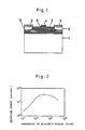
- FIG. 1 represents a novel FET related to this invention incorporating a channel layer comprised of a crystalline compound semiconductor multiple thin-film layer 2 containing each 6 layers of InAs and InP alternately being 0 0 laminated by about 69A and about 100A on the semiinsulated InP substrate 1.
- the multiple thin-film layer 2 has about 0.1 um thickness as a whole, which is formed on the semiinsulated InP substrate 1 by applying the MBE growth method.
- the surface of the multiple thin-film layer 2 is provided with the evaporated AuGeNi ohmic junction electrodes 3, to form the source electrode and drainage electrode.
- Gate electrode is made of the A1 Schottky junction electrode provided on the insulated layer 6 by evaporation.
- FIG. 2 is the chart denoting the result of evaluating the dependency of the drifting speed of electrons inside of the multiple thin-film layer 2 shown in FIG. 1 on the intensity of the applied electric field.
- the multiple thin-film layer 2 allows electrons to flow themselves at a specific speed almost corresponding to that is available inside of InAs.
- the multiple thin-film layer 2 doesn't cause impact ionization to occur even when high electric field is applied, while allowing electrons to flow themselves at a specific speed almost corresponding to that is available inside of InP.
- the dependency of the electron mobility on the intensity of electric field is significantly improved.
- the inventor observed satisfactory effect corresponding to those which are mentioned above.
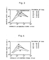
- the inventor confirmed the dependency of the drifting speed of electrons on the applied electric field by providing the thickness of the InAs layer at about 21A, 24A, 45A, 75A, and 78A (refer to e, c, b, a, and d shown in FIG. 3) against the thickness of the InP layer of about 100A.
- the InAs layer had thickness at about 21A, electrons flowed themselves at a low speed in low electric field application.
- the InAs layer had » thickness at about 78A, the drifting speed of electrons was increased until applied electric field rose to a certain level. When the applied electric field exceeded a certain critical level, the specimen was eventually destroyed. Taking this into account, the dependency of the electron mobility on the applied electric field can securely be improved by setting the thickness of the InAs 0 layer at a certain value between about 24A and a maximum of 75A. It was probable that, since the InAs layer had a too large thickness, preferential flow of electrons inside of the InP layer didn't occur even when high electric field was applied, thus causing a large amount of current to flow through only the InAs layer to eventually destroy the specimen.
- the inventor also achieved the identical effect by employing the well layer and the barrier layer respectively being composed of InAs and GaAs.
- Use of these layers composed of the latter components resulted in the lowered electron mobility in high electric field application, which was slower than those which are shown in FIGs. 2 and 3, while the electron mobility became almost equal to that was observed from the GaAs bulk crystal. This characteristic was observed only when the thickness of the InAs layer was varied from about 24A to about 60A.
- FIG. 4 is the chart denoting the result of evaluating the dependency of the drifting speed of electrons on the applied electric field when employing the well layer and the barrier layer respectively being composed of InAs and GaAs.
- the inventor confirmed the results shown in FIG. 4 by evaluating the dependency of the drifting speed of electrons on the applied electric field by providing the thickness of the InAs layer at about 21A, 24A, 60A, and 0 72A (refer to c, b, a, and d) against the thickness of the GaAs layer at about 50A.
- the InAs layer 0 has the thickness at about 21A under low electric field, electrons flow themselves at a low speed in low electric field application, and therefore, the InAs layer should be 0 provided with a minimum thickness at about 24A.
- the InAs layer 0 had the thickness at about 72A, a variety of defects took place with the specimen due to unsatisfactory surface condition of the tested specimen.
- the specimen generated mirror surface when the InAs layer had the thickness at about 21A, 24A, and 60A, respectively. Taking this into account, the dependency of the electron mobility on the applied electric field can securely be improved by providing the thickness of the InAs layer at from about 24A to about 60A.
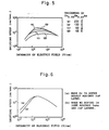
- FIG. 5 is the chart denoting the result of evaluating the dependency of the drifting speed of electrons on the applied electric field when employing the well layer and the barrier layer respectively being comprised of In 0.53 Ga 0.47 As and InP.
- the inventor confirmed the dependency of the drifting speed of electrons on the applied electric field by providing the thickness In 0.53 Ga 0.47 As layer at about 65 A, 68 A, 100A, and 200A (refer to d, c, b, and a shown in FIG. 4) against the thickness of InP layer at about 100A.
- the In 0.53 Ga 0.47 As layer should be provided with a minimum thickness at about 68A.
- the well layer may be comprised of either InAs or InSb and the barrier layer may also be comprised of InAsyP 1-y (0 ⁇ y ⁇ 1.0).
- the well layer may also be comprised of InAs y P 1-y (0.5 ⁇ y ⁇ 1.0) and the barrier layer may also be comprised of InAs y P 1-y (0 ⁇ y ⁇ 0.5).
- n-type impurities such as silicon (Si), tin (Sn), tellurium (Te), and the like against only the barrier layer portions of all those combinations mentioned above
- the inventor successfully promoted the electron mobility by 20% through a maximum of 50% in low electric field application.
- FIG. 6 is the chart denoting the results of evaluating the dependency of the drifting speed of electrons on the intensity of the applied electric field when using the well layer comprised of InAs crystal having the 0 thickness at about 75A and the barrier layer of InP cry-, stal having the thickness at about 100A.
- Reference character "a” in FIG. 6 indicates the result of the doping of silicon against only InP layer portion, whereas reference character “b” indicates the result without doping silicon against both InAs and InP layers.
- the thickness of the entire channel layer can be set in the submicron order. Accordingly, by effectively applying those constituents of the preferred embodiments to a variety of compound semiconductor devices for making up IC and LSI, it is possible for all the electronic elements to securely accelerate their operation speed independent of variable conditions of the applied electric field.
Landscapes
- Junction Field-Effect Transistors (AREA)
- Physical Deposition Of Substances That Are Components Of Semiconductor Devices (AREA)
Abstract
Description
- The present invention relates to a compound semiconductor device, more particularly, to a compound semiconductor device specially suited for manufacturing component device of integrated circuits (IC) and large-scale integrated circuits (LSI) among those compound semiconductor devices such as field effect transistors (FET), high electron movement transistors (HEMT) and the like.
- As fabricating method of compound semiconductor devices, particularly electronic devices, the epitaxial growth method is generally employed owing to the thin and uniform growth of layer and ease of control of constituent element composition ratio. Above all, the molecular beam epitaxial (MBE) growth method is known as one of the particularly noticed techniques recently. For example, a device utilizing the MBE growth method and thin layer periodic structure is described in details by W. T. Tsang in Nikkei Electronics No. 308, 163 (1983).
- According to this MBE growth method, the crystal growth speed can be controlled on a single atomic plane level (see J. P. van der Ziel et al., J. Appl. Phys., 48 (1977), p. 3018), and, furthermore, when combined with the reflective electron diffraction method, the composition of one atomic plane can be accurately controlled (see J. H. Neave et al., Appl. Phys. A 31, 1, 1983).
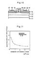
- By employing such MBE growth method, it is possible to fabricate a high electron mobility transistor (HEMT) as shown in Fig. 10.
- Incidentally, microwave elements using conventional compound semiconductors are disclosed, for example, in the Japanese Unexamined Patent Publication Nos. 4085/1984 and 147169/1983.
- In the HEMT structure shown in Fig. 10, a
GaAs layer 12 functioning as a buffer layer is formed on asemiinsulating GaAs substrate 11, and anundoped GaAs layer 13 serving as a channel layer is formed thereon. On theundoped GaAs layer 13 is formed anelectron supply layer 14 having a high impurity concentration such as n-Ga Al- As, and in the middle of theelectron supply layer 14 there is alayer 15 made of a semiconductor containing p-type impurities-at high concentration and possessing a large electrophilic ability, while agate electrode 16 is disposed on thislayer 15. Furthermore, thesurface region 17 of theelectron supply layer 14 at both sides of thelayer 15 is alloyed, and source anddrainage electrodes 18 are formed thereon. - In thus composed semiconductor device, when a proper bias voltage is applied to the
gate electrode 16, a two-dimensional electron gas 19 is formed at thechannel layer 13 side at the interface of theelectron supply layer 14 and thechannel layer 13. As a result, many electrons flow in the portion of a few tens angstrom units in thickness near the interface in thechannel layer 13 where only few impurity ions are present. Therefore, scatter of impurity ions which is one of major causes of limiting the electron mobility is less, so that a high electron mobility may be realized. - However, when operating such a conventional compound semiconductor device having the typical constitution mentioned above, the electron mobility is extremely dependent on the intensity of the electric field applied to the two-dimensional electron gas. High electron mobility is realized in low electric field application, conversely the electron mobility lowers in high electric field application. This phenomenon is described by M. Inoue et al. in J.J.A.P.22 357 (1983) for example. FIG. 11 shows one of these examples related to the constitution of the above- mentioned microwave element containing GaAs/n-GaxAl1-xAs, in which the above phenomenon is expressed by the broken- line curve.
- Generally, those phenomena including inter-valley scattering, impact ionization, or phonon scattering respectively cause electron scattering mechanism in a semiconductor device in high electric field application. Consequently, those characteristics specified below of the semiconductor crystals used for channel layers of ultrahigh-frequency transistors should be improved.
- (1) To prevent inter-valley scattering from occurrence, a greater value of energy difference ΔE should be provided between valleys of space K.
- (2) To prevent impact ionization from occurrence, a greater value should be provided for energy gap Eg.
- (3) To minimize loss of operating energy of carrier electrons caused by phonon scattering, a lesser value should be provided for effective mass m*.
- FIG. 7 shows an example of the energy band structure of GaAs crystals in conjunction with parameters of energy difference AE between valleys and energy gap Eg.
- Conventionally, GaAs, InP, and In0.53Ga0.47As respec- tively make up compound semiconductors for composing channel layers of conventional FET and HEMT. Table 1 represents approximate values of energy difference AE between valleys, energy gap Eg, and the effective mass m* of electrons of those compound semiconductors mentioned above. With reference to the later description, data related to InAs and InSb are also shown in Table 1: Note that the energy difference between valleys of In0.53Ga0.47As is not yet known.

- As is clear from Table 1, if the channel layer is composed of GaAs compound, since there is large energy gap Eg, impact ionization rarely takes place in high electric field application. Conversely, due to small energy difference ΔE between valleys, inter-valley scattering easily takes place. Furthermore, since the effective mass m* of electrons inherent to GaAs is great, a greater amount of operating energy of electrons is lost by phonon scattering, thus preventing electrons from flowing themselves faster. On the other hand, if the channel layer is composed of InP compound, due to substantial values of energy gap Eg, energy differences ΔETL, ΔETX between valleys inherent to Inp, neither impact ionization nor inter-valley scattering easily occurs in high electric field application, thus allowing electrons to flow . themselves at a faster speed. Conversely, since the effective mass m* of electrons inherent to InP is great, electrons are presented from flowing themselves at a faster speed in low electric field application. On the other hand, if the channel layer is composed of compound semiconductors made from InAs or InSb, due to small amount of effective mass m*, electrons flow themselves at an extremely fast speed in low electric field application. Conversely, since the energy gap Eg is small, impact ionization easily occurs in high electric field application. For example, impact ionization occurs in the compound semiconductor made of InAs in about 3.3 KV/cm electric field application. Further, if the channel layer- is composed of compound semiconductors made of the mixed crystals of In0.53Ga0.47As, this mixture exhibits a specific characteristic which is between those of compound semiconductor made of InAs and compound semiconductor made of GaAs. Those features thus far described above are apparently identified by referring to FIG. 12 showing the results of tests and theoretical development in conjunction with the dependency of the drift speed of electrons present in compound semiconductors on the intensity of electric field applied thereto. Results of evaluating the characteristic of compound semiconductors made of GaAs are cited by Ruch. J.G. and Kino G.S. in the Phys. Rev., 174, 921 (1969), and by Houston P.A. et al. in Solid State Comm., 20,197 (1977), respectively. Likewise, results of evaluating the characteristic of compound semiconductors made of InP are cited by Nelsen L.D. in the Phys. Lett., A38, 221 (1972) and Boers P.M. in the Electron Lett., 7, 625 (1971), respectively. Results of evaluating the characteristic'of compound semiconductors made of InAs are cited by Itoh et al. in the report ED83-77, (1983) presented to Electronic Communication Society of Japan. Covering the results of evaluating the characteristic of compound semiconductors made of InSb, refer to the reports presented by Glicksman M. et al. in the Phys. Rev., 129, 1572 (1963), Neukermans A. et al. in the Appl. Phys. Lett., 17, 102 (1970), and Smith J. et al. in the Appl. Phys. Lett., 37, 797 (1980), respectively. Results of evaluating the characteristic of compound semiconductors made of mixed crystals of InxGal-xAs are cited by Itoh et al. in the report ED83-77, (1983) presented to Electronic Communication Society of Japan.
- Generally, when operating either an FET or an HEMT, since either of these is subjected to several kilovolts per centimeter of electric field, any of these transistors having a conventional structure using channel layers made of InAs or InSb which easily allow occurrence of impact ionization in low electric field incurs much disadvan- , tages. Actually, there is no satisfactory FET incorporating channel layers made of either InAs or InSb. In other words, any of these conventional transistors cannot effectively apply advantageous characteristic of InAs or InSb which allows electrons to flow themselves at an extremely fast speed in low electric field application. Although not shown in FIG. 12, those compound semiconductors made of mixed crystals of InxGa1-xAs (0 < x < 1.0) or InAsyP1-y (0 < y < 1.0) vary their dependency of the electron mobility on the intensity of electric field according to values of x and y. However, the electron mobility of these compound semiconductors.is lower than that of those which are made of InAs in low electric field application, and yet, the electron mobility of these is also lower than that of those which are made of either GaAs or InP in high electric field application, respectively.
- In order to securely manufacture high-performance transistors featuring faster operating speed and more satisfactory characteristics, those transistors should allow electrons to flow themselves at an extremely fast speed even in low electric field application. Taking this into account, neither GaAs having the low electron mobility in high electric field application nor InP having the low electron mobility in low electric field application is ideally suited for making up channel layers, respectively. ,
- A study on a new constitution called "super-lattice constitution" has been underway, the detail of which is presented by L. Esaki, R. Tsu; IBM J. Res. Develop. (1970) P 61 for example. As shown in FIG. 8, using an adequate growth system like MBE growth method for example, thin-film layers made of compound semiconductors comprising different components like GaAs and AlAs for example are alternately and periodically laminated. By comparative evaluation of bulk crystals, specifically quantized levels are then generated in the thin-film layers in the lower portions of the conduction band (which are substantially layers A shown in FIG. 8 and are hereinafter called "well layers"). Although FIG. 8 shows only two
levels - Furthermore, the probability of the presence of electrons in these quantized levels is described by M. Jaros, K.B. Wong; J. Phys. C: Solid State Phys., 17 (1984) L765 for example. Assume that the barrier layer is made of Ga0.8Al0.2As and the well layer is made of GaAs, respectively, then, as shown in FIG. 9-a, only the quantized
levels level 3 exceeds the barrier height EB of the barrier layer made of Ga0.8Al0.2As. FIG. 9-b denotes that there is the greater probability of the presence of electrons on the side of GaAs layer atlevels - Taking the above conditions into account, the inventor detected that specific energy band structure identical to those which are shown in FIGS. 8 and 9 could be generated by making up the well layer by using either InAs or InSb and the barrier layer by using either InP or GaAs. First, when making up the well layer and the barrier layer by using InAs and InP, respectively, the inventor detected that the quantized level could be formed inside of the InAs layer. 'The inventor also detected that only the low-
energy levels energy level 3 could be raised to a point higher than the barrier height EB between InP and InAs as shown in FIG. 9. As a result, since the effective energy gap Eg inside of the InAs layer is equal to the difference between thequantized level 1 inside of the- conduction band and the quantizedlevel 1 inside of the valence band shown in FIG. 8, this energy gap becomes greater than the essential energy gap Eg of the InAs crystal. Consequently, as described earlier, impact ionization cannot easily take place, thus allowing high electric field of greater magnitude to be applied. Alternatively, in the presence of a specific intensity of electric field prior to the occurrence of impact ionization, the probability of the presence of highly energized electrons can significantly grow on the part of the InP layer (refer to the state oflevel 3 shown in FIG. 9) - Consequently, it is possible for the InAs layer to securely prevent impact ionization from internally taking place. In addition, since those electrons transitted into the InP layer in high electric field application follow the electric characteristic of the InP layer in high electric field application, as shown in FIG. 12, electrons flow themselves through the InP layer at a speed faster than that of those electrons flowing through other crystals even when high electric field is applied. In other words, in low electric field application, since electrons are confined inside of the InAs layer, electrons flow themselves at a speed faster than those electrons flowing through the GaAs and InP bulk crystals, and yet, since- highly-energized electrons transit themselves into the InP layer in high electric field application, electrons are allowed to flow themselves at a speed faster than those which flow through the GaAs crystal.
- This invention is contrived in the light of the above problems, it is hence a primary object of this invention is to present a novel compound semiconductor device having channel layer made of periodically laminated thin-film constitution capable of moving electrons at an extremely fast speed independent of the intensity of electric field.
- Another object of the invention is to provide a novel compound semiconductor device having channel layer made of periodically laminated thin-film constitution which prevents occurrence of inter-valley scattering and impact ionization.
- To achieve the above objects, the compound semiconductor device related to this invention comprised channel layer made of periodically laminated compound semiconductor thin-films substantially being different from each other. The energy difference between the conduction band and the valence band of the compound semiconductor thin-film layers of one side making up said channel layer is less than that of the compound semiconductor thin-film- layers of the other side, moreover the electron mobility in low electric field application of one side compound semiconductor thin-film layers is greater than that of the other side, besides, the electron mobility in high electric field application is less than that of the other side compound semiconductor thin-film layers, and/or the impact ionization of the valence electron generated in high electric field application takes place earlier than the other side compound semiconductor thin-film layers. The energy difference between the conduction band and the valence band of the other side compound semiconductor thin-film layers is less than that of the one side compound semiconductor thin-film layers, and yet, the electron mobility in high electric field application is greater than that of the other side thin-film layers. When low electric field is applied, conduction electrons preferentially flow through the one side compound semiconductor thin-film layers, whereas the highly-energized conduction electrons by acceleration preferentially flow through the other side compound semiconductor thin-film layers. Furthermore, before causing conduction electrons to generate impact ionization of valence electrons and inter-valley scattering in the conduction band of conduction electrons in the compound semiconductor thin-film layers of one side, conduction electrons which are highly energized by acceleration generated by the applied high electric field are allowed to smoothly transit themselves from compound semiconductor thin-film layers of one side to the other side compound semiconductor thin-film layers.
- The compound semiconductor thin-film layers of the other side may be of the constitution containing doped n-type impurities. Furthermore, the compound semiconductor thin-film layers of one side may be of compound semiconductors made of InAs or InSb, whereas the compound semiconductor thin-film layers of the other side may be of compound semiconductors made of InP or GaAs, respectively. Alternatively, compound semiconductor thin-film layers of one side may be of compound semiconductors made of mixed crystals of InxGa1-xAs (0 ≦ x < 1.0), whereas compound semiconductor thin-film layers of the other side may be made of InP. Furthermore, compound semiconductor thin-film layers of one side may be of compound semiconductors made of either InAs or InSb, whereas compound semiconductor thin-film layers of the other side may be of compound semiconductors made of mixed crystals of InAs yP1-y (0 < y < 1.0). Alternatively, compound semiconductor thin-film layers of one side may be of compound semiconductors made of mixed crystals of InAsyP1-y (0.5 < y < 1.0), whereas the other side compound semiconductor thin-film layers may be of compound semiconductors made of mixed crystals of InASyP1-y (0 < y < 0.5), respectively.
- Since the compound semiconductor device related to this invention featuring the constitution mentioned above is made up channel layers by periodically laminating compound semiconductor thin-film layers of one side and the other side compound semiconductor thin-film layers, it is possible for the device to effectively generate energy gap having a specific magnitude enough to prevent impact ionization from occurrence in the compound semiconductor thin-film layers of one side, and/or promote the probability of the presence of highly energized electrons enough to completely prevent impact ionization from occurrence in . the compound semiconductor thin-film layers of the other side.
- Furthermore, since the device related to this invention causes conduction.'electrons to be confined in the compound semiconductor thin-film layers of one side in low electric field application in order that the conduction electrons can preferentially flow through the compound semiconductor thin-film layers of one side, these conduction electrons are allowed to move themselves at a significantly accelerated speed. Likewise, since the device related to this invention allows the highly energized conduction electrons to preferentially flow through the other side compound semiconductor thin-film layers after being accelerated by the applied high electric field, the mobility of these electrons can eventually and significantly be accelerated.
- In particular, before causing the conduction electrons to generate impact ionization of valence electrons and before occurrence of inter-valley scattering in the conduction band by the conduction electrons, the device related to this invention allows the highly energized conduction electrons accelerated by the applied high electric field to transit themselves from the compound semiconductor thin-film layers of one side to the other side compound semiconductive thin-film layers, and as a result, , the conduction electrons can preferentially flow through the other side compound semiconductor thin-film layers at a significantly accelerated speed.
- The invention will be better understood from the detailed description given hereinbelow and the accompanying drawings which are given by way of illustration only, and thus are not limitative of this invention in which:
- FIG. 1 is the simplified sectional diagram denoting a preferred embodiment of FET as the compound semiconductor device related to the invention;
- FIG. 2 is the chart denoting the result of evaluating the dependency of the drifting speed of electron in the FET shown in FIG. 1 on the intensity of the applied electric field;
- FIG. 3 is the chart denoting the result of evaluating the dependency of the drifting speed of electron on the intensity of the applied electric field when varying the thickness of the well layer comprised of InAs against the barrier layer comprised of InP;
- FIG. 4 is the chart denoting the result of evaluating the dependency of the drifting speed of electron on the intensity of the applied electric field when varying the thickness of the well layer comprised of InAs against the . barrier layer comprised of GaAs;
- FIG. 5 is the chart denoting the result of evaluating the dependency of the drifting speed of electron on the intensity of the applied electric field when varying the thickness of the well layer comprised of In0.53Ga0.47As against the barrier layer comprised of InP;
- FIG. 6 is the chart denoting the result of evaluating the dependency of the drifting speed of electron when silicon is doped against the barrier layer comprised of InP against the well layer comprised of InAs and also when neither of these layers is doped with silicon; .
- FIG. 7 is the chart denoting the energy band constitution of the compound semiconductor;
- FIG. 8 is the chart of energy composition for explaining the quantized level;
- FIG. 9 is the chart explaining the phenomenon in which highly energized electrons transit themselves from the well layer to the barrier layer;
- FIG. 10 is the simplified sectional diagram of a conventional HEMT;
- FIG. 11 is the chart denoting the result of evaluating the dependency of the electron mobility on the intensity of the applied electric field proper to a conventional HEMT; and
- FIG. 12 is the chart denoting the result of evaluat- . ing the dependency of the drifting speed of electron of a variety of conventional compound semiconductors on the intensity of the applied electric field.
- Referring now more particularly to the accompanying drawings, one of the preferred embodiments of this invention is described below.
- FIG. 1 represents a novel FET related to this invention incorporating a channel layer comprised of a crystalline compound semiconductor multiple thin-
film layer 2 containing each 6 layers of InAs and InP alternately being 0 0 laminated by about 69A and about 100A on thesemiinsulated InP substrate 1. The multiple thin-film layer 2 has about 0.1 um thickness as a whole, which is formed on thesemiinsulated InP substrate 1 by applying the MBE growth method. - The surface of the multiple thin-
film layer 2 is provided with the evaporated AuGeNiohmic junction electrodes 3, to form the source electrode and drainage electrode. Gate electrode is made of the A1 Schottky junction electrode provided on theinsulated layer 6 by evaporation. - Due to the evaporation and alloying processes done for generating the AuGeNi
ohmic junction electrode 3, the . Au atoms diffuse itself throughout the crystalline multiple thin-film layer 2 of compound semiconductor. As a result, periodic characteristic of the layer structure in the compound semiconductor crystalline multiple thin-film layer 2 goes out of order, thus causing the crystalline structure in thearea 5 to eventually become identical to the conventional InAsyP1-y mixed crystal. Consequently, the energy band structure in thisarea 5 also becomes identical to that of the conventional InAsyP1-y mixed crystal. Due to these phenomena took place during tests, the inventor smoothly formed ohmic junction. N. Holonyak et al. already announced similar phenomenon in which the diffusion of the atoms causes the destruction of the peri-- odic characteristic of the layer structure of compound semiconductor multiple thin-film layers in A.P.L. 39 (1981) 102. - By applying conventional techniques for making up conventional FET structures, the inventor confirmed that the
source electrode 3,drainage electrode 3, and thegate electrode 4 shown in FIG. 1 properly executed functions needed for FET. - FIG. 2 is the chart denoting the result of evaluating the dependency of the drifting speed of electrons inside of the multiple thin-
film layer 2 shown in FIG. 1 on the intensity of the applied electric field. As is clear from . the comparison to FIG. 12, while low electric field is applied, the multiple thin-film layer 2 allows electrons to flow themselves at a specific speed almost corresponding to that is available inside of InAs. In addition, the multiple thin-film layer 2 doesn't cause impact ionization to occur even when high electric field is applied, while allowing electrons to flow themselves at a specific speed almost corresponding to that is available inside of InP. In other words, by implementing the multiple thin-film layer constitution shown in FIG. 1, the dependency of the electron mobility on the intensity of electric field is significantly improved. In addition, by varying the 0 thickness of the InAs thin-film layer from about 24A to 0 about 75A, the inventor observed satisfactory effect corresponding to those which are mentioned above. Concretely, the inventor confirmed the dependency of the drifting speed of electrons on the applied electric field by providing the thickness of the InAs layer at about 21A, 24A, 45A, 75A, and 78A (refer to e, c, b, a, and d shown in FIG. 3) against the thickness of the InP layer of about 100A. When the InAs layer had thickness at about 21A, electrons flowed themselves at a low speed in low electric field application. Conversely, when the InAs layer had » thickness at about 78A, the drifting speed of electrons was increased until applied electric field rose to a certain level. When the applied electric field exceeded a certain critical level, the specimen was eventually destroyed. Taking this into account, the dependency of the electron mobility on the applied electric field can securely be improved by setting the thickness of theInAs 0 layer at a certain value between about 24A and a maximum of 75A. It was probable that, since the InAs layer had a too large thickness, preferential flow of electrons inside of the InP layer didn't occur even when high electric field was applied, thus causing a large amount of current to flow through only the InAs layer to eventually destroy the specimen. - Although the above preferred embodiment employed the well layer and the barrier layer respectively being composed of InAs and InP, the inventor also achieved the identical effect by employing the well layer and the barrier layer respectively being composed of InAs and GaAs. Use of these layers composed of the latter components resulted in the lowered electron mobility in high electric field application, which was slower than those which are shown in FIGs. 2 and 3, while the electron mobility became almost equal to that was observed from the GaAs bulk crystal. This characteristic was observed only when the thickness of the InAs layer was varied from about 24A to about 60A.
- FIG. 4 is the chart denoting the result of evaluating the dependency of the drifting speed of electrons on the applied electric field when employing the well layer and the barrier layer respectively being composed of InAs and GaAs. The inventor confirmed the results shown in FIG. 4 by evaluating the dependency of the drifting speed of electrons on the applied electric field by providing the thickness of the InAs layer at about 21A, 24A, 60A, and 0 72A (refer to c, b, a, and d) against the thickness of the GaAs layer at about 50A. Concretely, when the
InAs layer 0 has the thickness at about 21A under low electric field, electrons flow themselves at a low speed in low electric field application, and therefore, the InAs layer should be 0 provided with a minimum thickness at about 24A. - According to the test results, when the
InAs layer 0 had the thickness at about 72A, a variety of defects took place with the specimen due to unsatisfactory surface condition of the tested specimen. However, the specimen generated mirror surface when the InAs layer had the thickness at about 21A, 24A, and 60A, respectively. Taking this into account, the dependency of the electron mobility on the applied electric field can securely be improved by providing the thickness of the InAs layer at from about 24A to about 60A. - Of the multiple thin-
film layer 2 of the FET shown in FIG. 1, when using well layers which are respectively comprised of In0.53Ga0.47As and provided with the thick- ness at minimum of about 68A against the barrier layer comprised of InP, the inventor confirmed that the electron mobility in high electric field application was almost equal to that was shown in the InP. - FIG. 5 is the chart denoting the result of evaluating the dependency of the drifting speed of electrons on the applied electric field when employing the well layer and the barrier layer respectively being comprised of In0.53Ga0.47As and InP. Concretely, the inventor confirmed the dependency of the drifting speed of electrons on the applied electric field by providing the thickness In0.53Ga0.47As layer at about 65A, 68A, 100A, and 200A (refer to d, c, b, and a shown in FIG. 4) against the thickness of InP layer at about 100A. When the layer comprised of In0.53Ga0.47As had the thickness at about 65A, the drifting speed of electrons slowed down in low electric field application, and thus, the In0.53Ga0.47As layer should be provided with a minimum thickness at about 68A.
- When using the well layer comprised of InSb against the barrier layer comprised of GaAs or InP, the inventor confirmed that satisfactory result identical to that of FIG. 2 was obtained. When low electric field was applied, electrons flow themselves at a speed almost equal to the electron mobility inside of the InSb. Likewise, when high electric field was applied, electrons flowed themselves at a speed almost equal to the electron mobility inside of GaAs or InP. It was also confirmed from these experiments that impact ionization was completely prevented from occurrence inside of the InSb layer.
- The invention also provides other constitutions, in which the well layer may be comprised of either InAs or InSb and the barrier layer may also be comprised of InAsyP1-y (0 < y < 1.0). In addition, the well layer may also be comprised of InAs yP1-y (0.5 < y < 1.0) and the barrier layer may also be comprised of InAs yP1-y (0 < y < 0.5).
- As a result of doping n-type impurities such as silicon (Si), tin (Sn), tellurium (Te), and the like against only the barrier layer portions of all those combinations mentioned above, the inventor successfully promoted the electron mobility by 20% through a maximum of 50% in low electric field application.
- FIG. 6 is the chart denoting the results of evaluating the dependency of the drifting speed of electrons on the intensity of the applied electric field when using the well layer comprised of InAs crystal having the 0 thickness at about 75A and the barrier layer of InP cry-, stal having the thickness at about 100A. Reference character "a" in FIG. 6 indicates the result of the doping of silicon against only InP layer portion, whereas reference character "b" indicates the result without doping silicon against both InAs and InP layers. By referring to these results, the inventor eventually- confirmed the effect described above.
- As is clear from the foregoing description of the preferred embodiments of this invention, the thickness of the entire channel layer can be set in the submicron order. Accordingly, by effectively applying those constituents of the preferred embodiments to a variety of compound semiconductor devices for making up IC and LSI, it is possible for all the electronic elements to securely accelerate their operation speed independent of variable conditions of the applied electric field.
- Although the foregoing description of the preferred embodiments totally refers to the use of FET, it is obvious for those skilled in the art that the constituents of the. invention can securely generate the same characteristics as the above by effectively being applied to other compound semiconductor devices like HEMT and others.
Claims (9)
Applications Claiming Priority (2)
| Application Number | Priority Date | Filing Date | Title |
|---|---|---|---|
| JP61099928A JPS62256478A (en) | 1986-04-30 | 1986-04-30 | Compound semiconductor device |
| JP99928/86 | 1986-04-30 |
Publications (3)
| Publication Number | Publication Date |
|---|---|
| EP0243953A2 true EP0243953A2 (en) | 1987-11-04 |
| EP0243953A3 EP0243953A3 (en) | 1990-04-25 |
| EP0243953B1 EP0243953B1 (en) | 1993-01-13 |
Family
ID=14260410
Family Applications (1)
| Application Number | Title | Priority Date | Filing Date |
|---|---|---|---|
| EP87106250A Expired - Lifetime EP0243953B1 (en) | 1986-04-30 | 1987-04-29 | Compound semiconductor device |
Country Status (6)
| Country | Link |
|---|---|
| US (1) | US4894691A (en) |
| EP (1) | EP0243953B1 (en) |
| JP (1) | JPS62256478A (en) |
| AU (1) | AU602143B2 (en) |
| CA (1) | CA1277440C (en) |
| DE (1) | DE3783507T2 (en) |
Cited By (2)
| Publication number | Priority date | Publication date | Assignee | Title |
|---|---|---|---|---|
| EP0481555A1 (en) * | 1990-10-19 | 1992-04-22 | Philips Electronics Uk Limited | Heterostructure field-effect transistor |
| US5856287A (en) * | 1995-03-01 | 1999-01-05 | Colgate-Palmolive Co. | Laundry concentrates |
Families Citing this family (12)
| Publication number | Priority date | Publication date | Assignee | Title |
|---|---|---|---|---|
| US5227644A (en) * | 1989-07-06 | 1993-07-13 | Nec Corporation | Heterojunction field effect transistor with improve carrier density and mobility |
| US5633512A (en) * | 1990-05-23 | 1997-05-27 | Canon Kabushiki Kaisha | Semiconductor device for varying the mobility of electrons by light irradiation |
| JP2919581B2 (en) * | 1990-08-31 | 1999-07-12 | 三洋電機株式会社 | Speed modulation transistor |
| JP2786327B2 (en) * | 1990-10-25 | 1998-08-13 | 三菱電機株式会社 | Heterojunction field effect transistor |
| CA2078540A1 (en) * | 1991-09-17 | 1993-03-18 | So Tanaka | Superconducting thin film formed of oxide superconductor material, superconducting device utilizing the superconducting thin film |
| US5274246A (en) * | 1992-05-04 | 1993-12-28 | The United States Of America As Represented By The Secretary Of The Air Force | Optical modulation and switching with enhanced third order nonlinearity multiple quantum well effects |
| JP3141838B2 (en) * | 1998-03-12 | 2001-03-07 | 日本電気株式会社 | Field effect transistor |
| US6897472B2 (en) * | 2003-06-26 | 2005-05-24 | Rj Mears, Llc | Semiconductor device including MOSFET having band-engineered superlattice |
| US6878576B1 (en) * | 2003-06-26 | 2005-04-12 | Rj Mears, Llc | Method for making semiconductor device including band-engineered superlattice |
| TWI404209B (en) * | 2009-12-31 | 2013-08-01 | Univ Nat Chiao Tung | High electron mobility transistor and manufacturing method thereof |
| US8690134B1 (en) | 2012-06-06 | 2014-04-08 | Ben J. Saam | Equipment support rack assembly |
| WO2014017063A1 (en) * | 2012-07-24 | 2014-01-30 | 住友化学株式会社 | Semiconductor substrate, method for manufacturing semiconductor substrate, and method for manufacturing composite substrate |
Family Cites Families (6)
| Publication number | Priority date | Publication date | Assignee | Title |
|---|---|---|---|---|
| US4194935A (en) * | 1978-04-24 | 1980-03-25 | Bell Telephone Laboratories, Incorporated | Method of making high mobility multilayered heterojunction devices employing modulated doping |
| JPS58178572A (en) * | 1982-04-14 | 1983-10-19 | Hiroyuki Sakaki | Mobility modulation type field effect transistor |
| US4797716A (en) * | 1984-04-04 | 1989-01-10 | The United States Of America As Represented By The United States Department Of Energy | Field-effect transistor having a superlattice channel and high carrier velocities at high applied fields |
| JPS61172381A (en) * | 1984-12-22 | 1986-08-04 | Fujitsu Ltd | Inp group compound semiconductor device |
| US4697197A (en) * | 1985-10-11 | 1987-09-29 | Rca Corp. | Transistor having a superlattice |
| JP2557373B2 (en) * | 1986-04-05 | 1996-11-27 | 住友電気工業株式会社 | Compound semiconductor device |
-
1986
- 1986-04-30 JP JP61099928A patent/JPS62256478A/en active Granted
-
1987
- 1987-04-24 CA CA000535564A patent/CA1277440C/en not_active Expired - Lifetime
- 1987-04-24 US US07/042,330 patent/US4894691A/en not_active Expired - Fee Related
- 1987-04-29 DE DE8787106250T patent/DE3783507T2/en not_active Expired - Fee Related
- 1987-04-29 EP EP87106250A patent/EP0243953B1/en not_active Expired - Lifetime
- 1987-05-08 AU AU72653/87A patent/AU602143B2/en not_active Ceased
Non-Patent Citations (6)
| Title |
|---|
| INTERNATIONAL ELECTRON DEVICES MEETING TECHNICAL DIGEST 5-7 December 1983, pages 696-698- Washington, DC; USA; T.E. ZIPPERIAN et al.: "An InO.2GaO.8As/GaAs, modulation-doped, strained-layer superlatice field-effect transistor" page 696,697 * |
| INTERNATIONAL ELECTRON DEVICES MEETING TECHNICAL DIGEST 5-7 December 1983, pages 696-698, Washington, DC; T.E. ZIPPERIAN et al.: "An In0.2Ga0.8As/GaAs, modulation-doped, stralend-layer superlatice field-effect transistor" * |
| JAPANESE JOURNAL OF APPLIED PHYSICS vol. 19, no. 9, September 1980, pages L551-L554, Tokyo, Japan; T. FUKUI et al.: "InAsSbP-InAs Superlattice Grown by Organometallic VPE Method" * |
| PHYSICAL REVIEW vol. 129, no. 4, 15 February 1963, page 1572 ff; M. GLICKSMAN et al.: "Hot Electrons in Indium Antimonide" * |
| PHYSICAL REVIEW vol. 174, no. 3, 15 October 1968, page 921 ff; J.G. RUCH et al.: "Transport Properties of GaAs" * |
| PHYSICS LETTERS vol. 38A, no. 4, 14 February 1972, pages 221,222; L.D. NIELSEN: "Microwave measurement of electron drift velocity in indium phosphide for electric fields up to 50 kV/cm" * |
Cited By (3)
| Publication number | Priority date | Publication date | Assignee | Title |
|---|---|---|---|---|
| EP0481555A1 (en) * | 1990-10-19 | 1992-04-22 | Philips Electronics Uk Limited | Heterostructure field-effect transistor |
| GB2248966A (en) * | 1990-10-19 | 1992-04-22 | Philips Electronic Associated | Field effect semiconductor devices |
| US5856287A (en) * | 1995-03-01 | 1999-01-05 | Colgate-Palmolive Co. | Laundry concentrates |
Also Published As
| Publication number | Publication date |
|---|---|
| AU602143B2 (en) | 1990-10-04 |
| JPH0354854B2 (en) | 1991-08-21 |
| EP0243953B1 (en) | 1993-01-13 |
| AU7265387A (en) | 1987-11-05 |
| DE3783507D1 (en) | 1993-02-25 |
| CA1277440C (en) | 1990-12-04 |
| EP0243953A3 (en) | 1990-04-25 |
| US4894691A (en) | 1990-01-16 |
| DE3783507T2 (en) | 1993-07-29 |
| JPS62256478A (en) | 1987-11-09 |
Similar Documents
| Publication | Publication Date | Title |
|---|---|---|
| KR940004417B1 (en) | High electro mobility transistor | |
| Ploog | Delta-(-) doping in MBE-grown GaAs: concept and device application | |
| EP0133342B1 (en) | A superlattice type semiconductor structure having a high carrier density | |
| Ploog et al. | Fundamental studies and device application of δ-doping in GaAs Layers and in AlxGa1− xAs/GaAs heterostructures | |
| US5285087A (en) | Heterojunction field effect transistor | |
| EP0243953A2 (en) | Compound semiconductor device | |
| EP0005059A2 (en) | A semiconductor device having a layered structure and a method of making it | |
| US5831296A (en) | Semiconductor device | |
| US7187045B2 (en) | Junction field effect metal oxide compound semiconductor integrated transistor devices | |
| JPS6342864B2 (en) | ||
| EP0594442A2 (en) | Schottky junction device | |
| EP0151309B1 (en) | High electron mobility field-effect transistor | |
| CA1290865C (en) | Hot electron transistor | |
| US5298441A (en) | Method of making high transconductance heterostructure field effect transistor | |
| JPH02292832A (en) | Resonant tunneling semicondu- -ctor device | |
| EP0042066B1 (en) | Intermetallic semiconductor devices | |
| KR920006434B1 (en) | Resonant Tunneling Barrier Structure Device | |
| US4600932A (en) | Enhanced mobility buried channel transistor structure | |
| JPH0661270A (en) | Semiconductor device manufacturing method and semiconductor device | |
| Zwicknagl et al. | Modulation of electronic properties in liquid phase epitaxially grown pnpn GaAs multilayers | |
| US5107314A (en) | Gallium antimonide field-effect transistor | |
| Nakagawa et al. | Anomalous mobility enhancement in Si doping superlattices | |
| EP0240953A2 (en) | Compound semiconductor device | |
| KR910006698B1 (en) | Semiconductor device | |
| JPS63136672A (en) | tunnel transistor |
Legal Events
| Date | Code | Title | Description |
|---|---|---|---|
| PUAI | Public reference made under article 153(3) epc to a published international application that has entered the european phase |
Free format text: ORIGINAL CODE: 0009012 |
|
| AK | Designated contracting states |
Kind code of ref document: A2 Designated state(s): DE FR GB NL |
|
| PUAL | Search report despatched |
Free format text: ORIGINAL CODE: 0009013 |
|
| AK | Designated contracting states |
Kind code of ref document: A3 Designated state(s): DE FR GB NL |
|
| 17P | Request for examination filed |
Effective date: 19900606 |
|
| 17Q | First examination report despatched |
Effective date: 19910813 |
|
| GRAA | (expected) grant |
Free format text: ORIGINAL CODE: 0009210 |
|
| AK | Designated contracting states |
Kind code of ref document: B1 Designated state(s): DE FR GB NL |
|
| REF | Corresponds to: |
Ref document number: 3783507 Country of ref document: DE Date of ref document: 19930225 |
|
| ET | Fr: translation filed | ||
| PLBE | No opposition filed within time limit |
Free format text: ORIGINAL CODE: 0009261 |
|
| STAA | Information on the status of an ep patent application or granted ep patent |
Free format text: STATUS: NO OPPOSITION FILED WITHIN TIME LIMIT |
|
| 26N | No opposition filed | ||
| PGFP | Annual fee paid to national office [announced via postgrant information from national office to epo] |
Ref country code: FR Payment date: 19960410 Year of fee payment: 10 |
|
| PGFP | Annual fee paid to national office [announced via postgrant information from national office to epo] |
Ref country code: GB Payment date: 19960422 Year of fee payment: 10 |
|
| PGFP | Annual fee paid to national office [announced via postgrant information from national office to epo] |
Ref country code: DE Payment date: 19960429 Year of fee payment: 10 |
|
| PGFP | Annual fee paid to national office [announced via postgrant information from national office to epo] |
Ref country code: NL Payment date: 19960430 Year of fee payment: 10 |
|
| PG25 | Lapsed in a contracting state [announced via postgrant information from national office to epo] |
Ref country code: GB Effective date: 19970429 |
|
| PG25 | Lapsed in a contracting state [announced via postgrant information from national office to epo] |
Ref country code: NL Effective date: 19971101 |
|
| GBPC | Gb: european patent ceased through non-payment of renewal fee |
Effective date: 19970429 |
|
| PG25 | Lapsed in a contracting state [announced via postgrant information from national office to epo] |
Ref country code: FR Free format text: LAPSE BECAUSE OF NON-PAYMENT OF DUE FEES Effective date: 19971231 |
|
| PG25 | Lapsed in a contracting state [announced via postgrant information from national office to epo] |
Ref country code: DE Free format text: LAPSE BECAUSE OF NON-PAYMENT OF DUE FEES Effective date: 19980101 |
|
| NLV4 | Nl: lapsed or anulled due to non-payment of the annual fee |
Effective date: 19971101 |
|
| REG | Reference to a national code |
Ref country code: FR Ref legal event code: ST |