EP0243402B1 - Spezialrechner für getrennte ausführung mancher betriebssystemfunktionen in einem grossen datenverarbeitungssystem - Google Patents
Spezialrechner für getrennte ausführung mancher betriebssystemfunktionen in einem grossen datenverarbeitungssystem Download PDFInfo
- Publication number
- EP0243402B1 EP0243402B1 EP19860906170 EP86906170A EP0243402B1 EP 0243402 B1 EP0243402 B1 EP 0243402B1 EP 19860906170 EP19860906170 EP 19860906170 EP 86906170 A EP86906170 A EP 86906170A EP 0243402 B1 EP0243402 B1 EP 0243402B1
- Authority
- EP
- European Patent Office
- Prior art keywords
- event
- processes
- processor
- task
- processing system
- Prior art date
- Legal status (The legal status is an assumption and is not a legal conclusion. Google has not performed a legal analysis and makes no representation as to the accuracy of the status listed.)
- Expired
Links
Images


Classifications
-
- G—PHYSICS
- G06—COMPUTING OR CALCULATING; COUNTING
- G06F—ELECTRIC DIGITAL DATA PROCESSING
- G06F9/00—Arrangements for program control, e.g. control units
- G06F9/06—Arrangements for program control, e.g. control units using stored programs, i.e. using an internal store of processing equipment to receive or retain programs
- G06F9/46—Multiprogramming arrangements
- G06F9/48—Program initiating; Program switching, e.g. by interrupt
- G06F9/4806—Task transfer initiation or dispatching
- G06F9/4843—Task transfer initiation or dispatching by program, e.g. task dispatcher, supervisor, operating system
- G06F9/4881—Scheduling strategies for dispatcher, e.g. round robin, multi-level priority queues
Definitions
- This invention relates to a special purpose processor and more particularly to such a processor for offloading many operating system functions that would otherwise be executed by one or more central processors in a large data processing system.
- Multi-processing systems and a single processing system adapted for multi-programming require operating systems for the purpose of scheduling tasks on a particular processor, initiating input/output data transfers, handling external interrupts, and the like.
- Such operating systems sometimes called a master control program (MCP)
- MCP master control program
- Such particular processes and subroutines reside in main memory and currently must be executed by the particular central processors when a processor or another central processor in a multi-processing system requires service, such as when it has finished a particular process or task, requires an input/ output operation or some other service.
- the operating systems allocate and deallocate events where an event may be an external interrupt, I/O operation, etc.; implement a set of functions which may be performed upon these events; maintain the status of processes or tasks running on the system; perform task priority computations and schedule the execution of tasks by various central processors; maintain the system timers, including the interval timers; and perform some accounting and billing functions.
- EP-A-0 064142 discloses a task handling arrangement for a multiprocessor computer system in which each processor includes a task dispatcher and a signal dispatcher. Whenever a task runs in a processor, a task dispatcher element is put on a task dispatching queue. The signal dispatcher in each processor examines the queue to see if any processor is running a lower priority task. If so, a task switch is performed by signalling the selected processor to invoke its task dispatcher. After completing the task switch the selected processor must invoke its signal dispatcher to determine if the task it has been performing should now be performed on some other processor.
- the present invention relates to a data processing system having a plurality of main processing units which can communicate with at least one memory module by way of a memory controller, wherein said memory module, or at least one of said memory modules, stores operating system code for execution by said main processing units, and wherein said system includes task scheduling and allocating means,
- the invention is characterised in that said task scheduling and allocation is carried out by a task control processor which can communicate with any one of said main processing units by way of said memory controller and which includes input means which can receive from one of said main processing units a command indicating that the process currently being executed by that main processing unit is in a wait state, process table means for storing process designations of the processes scheduled to be executed by said system including processes which are available to be executed and arranged according to assigned priorities, output means coupled to said memory controller and to said process table means to transmit a move command to the main processing unit in said wait state to move execution by said unit to a different one of the processes stored in said memory module or modules, and control means coupled to said input means, said process table means, and said output means to cause said output means to transmit said move command together with the process designation of the next highest priority process that is available.
- FIG. 1 A large data processing system, and in particular a multi-processing system, which employs the present invention is illustrated in FIG. 1.
- the system includes a plurality of main processing units 10 and one or more 1/0 processors 11, each of which can communicate with a plurality of memory modules 12, by way of memory controller 12a.
- the present invention is an addition to the system in the form of task control processor 13 which also communicates with any one of processors 10 by way of controller 12a.
- While the present invention may be used in a conventional system of sequential or von Neumann type processors, the preferred embodiment of the present invention, as described below, is directed toward a system of processors designed for the execution of block-structured programming languages, i.e., nested declarations, which is a natural form for the expression of complex algorithms.
- a particular processor that was designed to employ such block-structured, or nested languages, is described in the Barton et al. U.S. Patents No. 3,461,434; 3,546,677 and 3,548,384.
- These patents describe a stack- oriented data processor where the stack mechanism, a first-in last-out mechanism, handles the flow of operators and associated parameters in a manner which reflects the nested structure of the particular higher level languages employed.
- Such languages include ALGOL and ALGOL-type languages, such as PU1, EULER, etc. (Cf., E. I. Organick Computer System Organization, Academic Press, 1973).
- a system of the type described in the above- identified Barton patents is oriented around the concept of a segmented memory and specially treated segments called stacks.
- the processor runs in an expression stack; operators take their arguments from the top of the stack and leave their results on the top of the stack.
- the data addressing space of the executing program is mapped into the stack as well as other stacks linked to it and data segments referenced by the descriptors contained in the stack structure.
- the addressing environment of the executing code stream consists of a set of local addressing spaces contained within the stacks. These are called activation records or lexical regions and each consists of a set of variables addressed by an index relative to the base of the activation record. That is to say, addressing of a given data item is by way of an address couple of the form (Lambda, Delta) where Lambda is the lexical level of a given activation record in the stack and Delta is the offset to the variable from the base of the activation record at level Lambda.
- the respective records, or lexical regions are linked together by pointers from the base of the topmost activation record to the lowest level activation record.
- addressing is optimized by defining an array of "display" registers in the processor which registers are maintained in such a manner that element i in the array contains the base of the activation record at the level i.
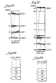
- FIG. 2A A data stack as might exist in one of memory modules 12 of FIG. 1 is illustrated in FIG. 2A and consists of four activation records at lexical levels 0-3, where the value of the topmost lexical level is stored in a lexical level register in a corresponding processor.
- the actual addresses in memory of the respective bases of the activation records are shown in 2A and these addresses are stored in the display registers of the corresponding processor in a manner illustrated in FIG. 2B.
- FIG. 2C illustrates that the processor is now working in a different stack or portion of memory.
- the display registers of a particular processor have had to be updated and this update is shown by the new contents of the display registers as shown in FIG. 2D.
- the task control processor 13 is designed to relieve the master control program of many of its most time consuming functions.
- the respective central processors 10 of FIG. 1 would be running various programs or processes. That is to say, they would be operating in different stacks in memory. If, for example, a particular processor executed a branch instruction which called for a branch to another task, it would notify the master control program which would then initiate the required process and cause the requesting process to be put in a waiting state. When the required process has been finished, the master control program would then notify the requesting process that the required process was finished and the requesting process would then be reactivated.
- Other examples of master control program functions have been discussed above, such as handling of external interrupts and initialization of input/output operations.
- the master control program in prior art systems would handle the scheduling of various tasks for execution by the various processors 10 of FIG. 1 according to which processes had the highest priority.
- Process table 21 and process statistics table 20b contain the information as to the status of all tasks or processes scheduled to be run on the system of FIG. 1. In the described embodiment of the present invention, there can be 4 K such tasks or processes running on the system at any one point in time.
- the status information of the processes in process table 21 are arranged as a queue or a linked list of processes according to the priority of the processes involved.
- Event table 20a is employed to contain information as to the status of various event designations called for by processes running on the system. In the described embodiment of the present invention, there may be a maximum of 512 K such events being utilized at any one time.
- a process being executed by a particular processor 10 of FIG. 1 requires an event designation, it requests the allocation of such a designation from the task control processor of FIG. 3, which then allocates an unallocated event designation to that process and sends an event token to be placed in main memory on the top of the particular stack whose process requested that event designation.
- Event table 20a then upgrades the event information to indicate that the event has been allocated.
- the event token is made up of the event address to event table 20a and also certain coded bits to ensure that one of processors 10 of FIG.
- Event table 20a is also employed to maintain a linked list of various processes requesting a particular event that has already been allocated and assigns that event to the highest priority process requesting that event when the event is freed or liberated by its owning process.
- Event table 20a serves the purpose of maintaining the status of the event, e.g., whether it is available for allocation, whether it has occurred, what processes are waiting on it, and so forth.
- support logic 22 is employed to insert information fields into event table 20a, statistics table 20b and link table 20c as well as to extract fields therefrom as required.
- Local memory 23 serves as an output buffer and also maintains a processor table which indicates which processes are currently running on the respective processors 10 of FIG. 1.
- Message transmission to the other processors of FIG. 1 are by way of memory controller 12a from output register 29 of FIG. 3. Messages are received from controller 12a by way of input register 25 to message buffer 24. As indicated in FIG. 3, the various functional units thus described have inputs to arithmetic logic unit module 26 by way of arithmetic logic unit input multiplexer 27. Arithmetic logic unit module 26 is employed to compute process priorities as described above and also to form messages for transmission to the other processors of the system.
- Clock timer 28 supplies real time clock values to arithmetic logic module 26 to aid in the computation of how long a particular process in a wait state has been waiting as compared to the maximum amount of time it can wait before its execution must be reactivated (as well as statistics, and task scheduling algorithms).
- All of the functional units of FIG. 3 are under the control of sequence control store 30 and are activated by the receipt of an external processor request by message buffer 24, where the request command is decoded by control store 30.
- the special purpose processor of the present invention responds by transmitting to that processor a MOVE-STACK command which causes the processor to begin executing a different process assigned by the special purpose processor of the present invention.
- This command is stored in local memory 23 of FIG. 3 and is transmitted to the processor which made the initial request along with the process number or stack number of the next available process having the highest priority for execution as will be more thoroughly described below.
- the task control processor of FIG. 3 serves to maintain the status of the various processes and control the execution of those processes by the respective central processors 10 of FIG. 1.
- a process may be in one of four main states as follows:
- the task control processor maintains two further state bits for each process, namely "scheduled” and "blocked".
- a scheduled process is one which is included in the scheduling mechanism and unscheduled when the process is to be removed from that mechanism.
- the four states listed above apply only to scheduled processes.
- a blocked process is one which will not be scheduled for execution on a processor until such time as it becomes "unblocked”.
- Process table 21 and statistics table 20b of FIG. 3 maintain the following information for each process in the system: the process current state, i.e., ready waiting, etc.; the process priority; accumulated processor and ready time; the processors to which the process may be assigned; maximum permitted processor time; and the class of service of the process.
- the process class is used to implement a resource sharing scheme between different groups of processes.
- the task control processor of FIG. 3 also maintains system wide statistics on processor utilization and processor time consumed by processes of different classes. These process attributes may be set and read by software at any time, regardless of whether the process is currently under the control of the task control processor.
- the task control process or FIG. 3 responds to process commands from the respective main processor.
- a SET-PRIORITY command changes the priority of a designated stack to a supplied value.
- a SET-CLASS command sets the statistics class of the designated stack.
- a SET-PROCESSOR command marks the designated stack as being executable only on a designated main processor.
- the INSERT command causes the designated stack to be included in the scheduling mechanism and the REMOVE command causes the designated stack to be deleted from the scheduling mechanism.
- the above commands are merely examples of the types of commands issued to the task control processor to control process scheduling and many other commands are employed but their description is not required here.
- DEALLOCATE causes the designated event to be returned to the pool of available events and there may be other processes which are either waiting on or attempting to procure the event in which case the requesting processor will be notified.
- the PROCURE command results in an attempt to procure a designated event on behalf of the process which is currently executing on the requesting processor. If the event is available, it will be marked as unavailable, the owner will be designated as the stack number is currently executing. If the event is unavailable, the process will be suspended, the base priority of the owning process will be adjusted such that it is at least as great as the contending process' base priority and the requesting processor will be rescheduled.
- the LIBERATE command causes the task control processor to pass ownership of the designated event to the highest priority process which has attempted to procure it. If no such process exists, the event is marked as available.
- the SIMPLE-WAIT command suspends execution of the process currently executing on the requesting processor until the designated event has happened.
- the MULTIPLE Wait command suspends execution of the process currently executing on the requesting processor until either a time limit has expired or one of a set of events has happened.
- the CAUSE command will "awaken" all processes which are currently waiting on a designated event.
- the event will be marked as happened unless either a reset option is used or there is some stack performing a particular function upon the event, in which case it will be left in the not-happened state. If the event is available and has contenders, the highest priority contender will be given ownership of the event.
- the SET command marks the designated event as happened without reactivating any process which may be waiting on it.
- All of the tables of FIG. 3 are initialized whenever a halt-load is performed on the system. After that the tables are not reloaded but are modified from time to time depending upon the commands the task control processor is executing.
- control store 30 of FIG. 3 causes the respective processors to begin execution in various designated stacks. Thereafter, control store 30 of FIG. 3 will cause individual processors to be rescheduled (moved to another stack) primarily when that processor has executed a wait-on- event command or a procure command as was discussed above. Control store 30 of FIG. 3 will also cause a processor to move to another stack whenever it determines that it has been operating in its current stack for more than a prescribed time.
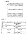
- FIG. 4 is a representation of the organization of process table 21 of FIG. 3 which is a static RAM with a capacity of 16K word locations of 17 bits each. This RAM is divided into 4K four-word blocks so as to provide the information required for the scheduling and manipulation of information for 4K processes as was described above. Each four-word block is addressed by a 12 bit process number, as was described above, which is supplied with 2 extra bits to select which of the words is to be addressed in the particular four-word block.
- FIG. 4B illustrates the format of one of the four-word blocks in FIG. 4A.
- bit 16 is the selectable bit which indicates that the process is a candidate for selection as head of the ready queue (which is described below). The process must be scheduled and ready and not blocked to be in this state.
- Bits 15-12 identify the statistics class to which class the current process belongs.
- Bits 11-0 are the ready queue forward link, which is used when chaining through the ready queue in order of descending priority. That is to say, bits 11-0 are the 12 bit process number or address to the process table of the next lower priority process in the linked list of such processes.
- Word-1 of FIG. 4 is similar to WORD-0 except that bits 11-0 now represent the ready queue reverse link or the process number of the next highest priority process in the linked list of processes scheduled on the system.
- bit 16 when set, indicates that this process is at the head of the ready queue for its particular processor designation as will be described in relation to WORD-3.
- Bits 15-8 of WORD-2 are the most significant portion of the total priority of the process which priority is setable by some processor task and is manipulated by the task control processor of the present invention.
- Bits 8-0 represent the least significant portion of the total priority of the process and are manipulated by the scheduling algorithm employed by the task control processor of the present invention.
- bit 16 when set, indicates whether or not the current process has been scheduled on the system.
- Bits 15-8 represent the original base priority of the process. This is the lowest base priority which the process would fall back to when lock contention conditions are resolved.
- Bits 7 and 6 indicate the type of processor upon which the current process is to be run (namely whether the processor is a main processor 10 of FIG. 1 or I/O processor 11 of FIG. 1, or a future processor type not yet implemented).
- Bits 5 and 4 represent the process state which may be Waiting, Ready, Selected (as was described above), and Alive.
- Bit 3 when set, indicates that the process has been "blocked” and task control processor will not schedule it for execution on a processor.
- Bit 2 when set, indicates that this process is to be interrupted on the next move stack command telling a processor to move to this stack number.
- Event table 20a of FIG. 3 contains storage locations of the status of 512K events. Like process table 21, each storage location in event table 20a is made up of a four-word block. The general formats of the respective words are illustrated in FIGS. 5A-D. Each block in the event table is addressed by an event number which is part of the event token, as was described above, along with two other bits which specify which of the four words is to be addressed. Each of the four words is 52 bits in width.
- FIG. 5A represents the general format of WORD-0. As illustrated therein, there are two principal fields that are relevant to this disclosure. Bits 31-24 indicate the priority of the highest priority process which is contending or trying to procure this event while it is owned by some other process for reasons that were described above. Bits 18-0 contain the event number of the next lower priority event owned by the process which owns the current event. That is to say, this field is a forward link in a queue of all events currently owned by the owner of the current event.
- FIG. 5B represents the general format of WORD-1 which is similar to that of WORD-0 except that bits 18-0 now represent the owner queue reverse link or the event number of the next highest priority event owned by the owner of the current event.
- FIG. 5C generally represents the format of WORD-2 which has two fields that are of particular interest here.
- Bits 35-24 contain the number of the current owning process.
- Bits 11-0 also represent a process number which represents the highest priority process which is attempting to procure ownership of the current event.
- FIG. 5D is a general format of WORD-3.
- Bit 51 of this word when set, indicates that the current event has been allocated.
- Bit 50 when set, indicates that the event is available.
- Bit 49 is a special bit which, when set, indicates that ownership of that event has been obtained by a particular authorized process andtaken away from all other processes that had had ownership.
- Bit 48 when set, indicates that the event has happened or occurred.
- Bit 47 when set, indicates that there are contenders or processes attempting to procure this event.
- Bit 46 when set, indicates that there are processes waiting for this event to happen. There are two other fields or sets of bits which are of significance to this disclosure.
- Bit 19-0 are a pointer or link to a list of processes which are waiting for the event to happen, which list is in link table 20c of FIG. 3.
- Bits 12-0 of this link are the process number of the first process in the list.
- WORDS 0, 1 and 2 are basically concerned with processes waiting to procure events while WORD-3 is basically concerned with processes which are waiting on events.
- processes waiting on an event it should be emphasized that only one process may own an event, or a plurality of events, at any one time. However, a number of processes can be waiting on a given event even though they don't own it. The reason for this is in the nature of the block-structured programming languages employed in the preferred embodiment of the present invention, as was discussed above in relation to FIGS. 2A-D. That is to say, with such block-structured languages, any process, although independent, is part of a hierarchy of processes.
- a given process when a given process requests and is allocated an event, it notifies its parent process that it owns that event and has assigned a function to it and the parent process in turn notifies other sibling processes that the particular event has been allocated and assigned a function. Any of the sibling processes requiring that event are then placed in a waiting state until the event occurs.
- FIG. 6 is a more detailed schematic diagram of arithmetic logic unit module 26 and arithmetic logic unit input multiplexer 27 of FIG. 3.
- arithmetic logic unit module 26 includes arithmetic logic unit 40 which receives inputs from B register 41 and accumulator 42.
- the output of arithmetic logic unit 40 is to rotator 43 which is a shifting mechanism that may shift left end around either eight bits or one bit.
- the output of rotator 43 is to accumulator 42.
- the output of B register 41 and accumulator 42 are also supplied to output multiplexer 44.
- the input to arithmetic logic unit module 26 is by way of the series of input multiplexers 27a and 27b which together form arithmetic logic unit input multiplexer 27 of FIG. 3. The inputs to these two multiplexers were described above in regard to FIG. 3.
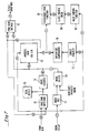
- FIG. 7 illustrates the input and output logic for process table 21 of FIG. 3.
- the actual process table is process RAM 50 which is a 16K by 18 bits (including parity) static random access memory. Addresses and data are received from arithmetic logic unit module 26 of FIG. 3 with the addresses going directly to process RAM input multiplexer 51 and the data going directly to the input of process RAM 50.
- Process RAM input multiplexer 51 selects either the address from the arithmetic logic unit module or from the output of process RAM 50 which address is a 12 bit process number as was described above. The selected address is then sent to address counter 52 for addressing process RAM 50.
- Two bits can also be received from sequence control store 30 of FIG. 3 by word register 53 of FIG. 7.
- these two bits specify which word in a particular process word-block is to be selected. These two bits may also come from a constant which selects the priority word of a particular process block and word select multiplexer 54 selects between either the constant or the contents of word register 53. These two bits are then added to the 12 bit output of address counter 12 to create a 14 bit address to process RAM 50.
- Magnitude comparator 56 serves to compare the priority of the current process block being addressed in process RAM 50 which a target priority as received by target priority register 57 from arithmetic logic unit module 26 of FIG. 3. This target priority represents the priority of a task to be inserted in the linked list of tasks being maintained in process RAM 50.
- Selectable task function unit 58 of FIG. 7 serves to compare the class of each of the processes in process RAM 50 with the contents of class enable mask 59 to see which of the current processes are enabled for execution on an available processor, in which case sequence control store 30 of FIG. 3 is notified by selectable task function 58.
- Mask control function unit 60 serves to set various bits in class enable mask 59 to indicate which classes can be run on currently available processors.
- FIG. 8 illustrates in more detail support logic 22 of FIG. 3 for receiving data for input into and fetching data from event table 20a, statistics table 20b and link table 20c of FIG. 3. All data transfers into and out of those tables is by way of staging register 70 which can receive data from the arithmetic logic unit module 26 of FIG. 3 or from respective tables themselves which are formed of dynamic RAMs. Staging register 70 can also receive data from its output and these three inputs are selected by input select unit 71. The data remains in staging register 70 for one clock period while its parity or error correction code (ECC) is checked by check/generator 74.
- ECC error correction code
- the data may then have fields extracted from it by field extraction unit 73 for transmission back to the arithmetic logic unit module or the entire output data from staging register 70 can be combined with a parity bit from check/generator 74 for transmission to the respective event table, link table or statistics table.
- the input to field extraction unit 73 is selected by field extract input multiplexer 72.
- Addresses for the respective tables are generated by address formation function unit 75 by receiving a 20 bit field from field extraction unit 73.
- An 8 bit literal from sequence control store 30 of FIG. 3 informs address formation function unit 75 of the particular table to be addressed and formation function unit 75 then forms the appropriate address for transmission to address counter 76 from which it is sent to the respective table by address source multiplexer 78 which may also select an address from refresh address counter 77 when the dynamic RAMs of tables 20a, 20b and 20c of FIG. 3 are being refreshed.
- FIG. 9A is a diagram of how ownership is passed from one process to the next lowest process waiting to procure an event.
- the P-head field of WORD-2 of the particular event block is used as a pointer to link table 20c of FIG. 3 where the process number of the next lower priority process requesting ownership resides.
- the event is then assigned this process as owner and this process is then made ready for the next available processor 10 of FIG. 1.
- that processor ecomes available it is given instruction to move to the stack number of the now owning process.
- the event again becomes available the above procedure is then repeated.
- FIG. 9B illustrates how link table 20c of FIG. 3 is employed to link processes waiting on this same event.
- the W-head of WORD-3 of the particular event block is employed to point both to the particular process block in process table 21 and also to the process link in link table 20c and this action ripples through the link table and the process table such that all processes waiting on that event are made ready for the next available processor 10 of FIG. 1.
- One advantage, among others, of the processor of the present invention is that external interrupts now vanish and the device requesting the interrupt, such as an 1/0 processor, merely signals the special purpose processor of the present invention that a specific event has occurred by sending a CAUSE command which causes that event to have its status changed to "has occurred”.
- a special purpose processor has been described above for the purpose of off-loading those operating system functions which consume most of the processing time of the various processors in a large data processing system.
- the special purpose processor is adapted to schedule processes or tasks on the various processors as the processors become available, which processes are scheduled according to their assigned priority.
- the special purpose processor also maintains an event table which is really a table of event designations to be allocated to different processes upon request when the requesting processes (including the operating system) assign a particular function to that event designation. The event table is then used to maintain the status of all such allocated events and to signal all processes waiting on a particular event that the event has happened.
Landscapes
- Engineering & Computer Science (AREA)
- Software Systems (AREA)
- Theoretical Computer Science (AREA)
- Physics & Mathematics (AREA)
- General Engineering & Computer Science (AREA)
- General Physics & Mathematics (AREA)
- Multi Processors (AREA)
Claims (7)
Priority Applications (3)
| Application Number | Priority Date | Filing Date | Title |
|---|---|---|---|
| EP89121828A EP0362903B1 (de) | 1985-10-15 | 1986-09-26 | Sonderzweckprozessor zur Übernahme vieler Betriebssystemfunktionen in einem grossen Datenverarbeitungssystem |
| EP89121835A EP0364000B1 (de) | 1985-10-15 | 1986-09-26 | Sonderzweckprozessor zur Übernahme vieler Betriebssystemfunktionen in einem grossen Datenverarbeitungssystem |
| AT86906170T ATE59714T1 (de) | 1985-10-15 | 1986-09-26 | Spezialrechner fuer getrennte ausfuehrung mancher betriebssystemfunktionen in einem grossen datenverarbeitungssystem. |
Applications Claiming Priority (6)
| Application Number | Priority Date | Filing Date | Title |
|---|---|---|---|
| US78766885A | 1985-10-15 | 1985-10-15 | |
| US787669 | 1985-10-15 | ||
| US787781 | 1985-10-15 | ||
| US06/787,669 US4779194A (en) | 1985-10-15 | 1985-10-15 | Event allocation mechanism for a large data processing system |
| US06/787,781 US4796178A (en) | 1985-10-15 | 1985-10-15 | Special purpose processor for off-loading many operating system functions in a large data processing system |
| US787668 | 1985-10-15 |
Related Child Applications (2)
| Application Number | Title | Priority Date | Filing Date |
|---|---|---|---|
| EP89121835A Division-Into EP0364000B1 (de) | 1985-10-15 | 1986-09-26 | Sonderzweckprozessor zur Übernahme vieler Betriebssystemfunktionen in einem grossen Datenverarbeitungssystem |
| EP89121828A Division-Into EP0362903B1 (de) | 1985-10-15 | 1986-09-26 | Sonderzweckprozessor zur Übernahme vieler Betriebssystemfunktionen in einem grossen Datenverarbeitungssystem |
Publications (2)
| Publication Number | Publication Date |
|---|---|
| EP0243402A1 EP0243402A1 (de) | 1987-11-04 |
| EP0243402B1 true EP0243402B1 (de) | 1991-01-02 |
Family
ID=27419841
Family Applications (3)
| Application Number | Title | Priority Date | Filing Date |
|---|---|---|---|
| EP19860906170 Expired EP0243402B1 (de) | 1985-10-15 | 1986-09-26 | Spezialrechner für getrennte ausführung mancher betriebssystemfunktionen in einem grossen datenverarbeitungssystem |
| EP89121828A Expired - Lifetime EP0362903B1 (de) | 1985-10-15 | 1986-09-26 | Sonderzweckprozessor zur Übernahme vieler Betriebssystemfunktionen in einem grossen Datenverarbeitungssystem |
| EP89121835A Expired - Lifetime EP0364000B1 (de) | 1985-10-15 | 1986-09-26 | Sonderzweckprozessor zur Übernahme vieler Betriebssystemfunktionen in einem grossen Datenverarbeitungssystem |
Family Applications After (2)
| Application Number | Title | Priority Date | Filing Date |
|---|---|---|---|
| EP89121828A Expired - Lifetime EP0362903B1 (de) | 1985-10-15 | 1986-09-26 | Sonderzweckprozessor zur Übernahme vieler Betriebssystemfunktionen in einem grossen Datenverarbeitungssystem |
| EP89121835A Expired - Lifetime EP0364000B1 (de) | 1985-10-15 | 1986-09-26 | Sonderzweckprozessor zur Übernahme vieler Betriebssystemfunktionen in einem grossen Datenverarbeitungssystem |
Country Status (4)
| Country | Link |
|---|---|
| EP (3) | EP0243402B1 (de) |
| CA (3) | CA1289674C (de) |
| DE (3) | DE3650160T2 (de) |
| WO (1) | WO1987002486A1 (de) |
Families Citing this family (11)
| Publication number | Priority date | Publication date | Assignee | Title |
|---|---|---|---|---|
| JPH0644234B2 (ja) * | 1987-07-17 | 1994-06-08 | 日本電気株式会社 | タスク管理装置 |
| US4985831A (en) * | 1988-10-31 | 1991-01-15 | Evans & Sutherland Computer Corp. | Multiprocessor task scheduling system |
| EP0466948B1 (de) * | 1990-07-16 | 1996-01-31 | Siemens Aktiengesellschaft | Kommunikationssystem mit einem der zentralen Steuerung dienenden Multiprozessorsystem |
| WO1992017796A1 (en) * | 1991-03-28 | 1992-10-15 | The Commonwealth Of Australia | Radar control task scheduling |
| US5485626A (en) * | 1992-11-03 | 1996-01-16 | International Business Machines Corporation | Architectural enhancements for parallel computer systems utilizing encapsulation of queuing allowing small grain processing |
| CA2128393C (en) * | 1992-12-23 | 2001-10-02 | Jean-Felix Perotto | Multi-tasking low-power controller |
| CN1209207A (zh) * | 1995-12-19 | 1999-02-24 | 艾利森电话股份有限公司 | 指令处理机作业的调度 |
| GB2308686A (en) * | 1995-12-20 | 1997-07-02 | British Aerospace | Integrated circuits for multi-tasking support in single or multiple processor networks |
| GB2367913A (en) * | 2000-09-16 | 2002-04-17 | Motorola Inc | Processor resource scheduler |
| FR2821940B1 (fr) * | 2001-03-12 | 2006-09-29 | Centre Nat Etd Spatiales | Procede et systeme de gestion du temps dans un systeme temps reel |
| US9547540B1 (en) | 2015-12-21 | 2017-01-17 | International Business Machines Corporation | Distributed operating system functions for nodes in a rack |
Family Cites Families (6)
| Publication number | Priority date | Publication date | Assignee | Title |
|---|---|---|---|---|
| US3548384A (en) | 1967-10-02 | 1970-12-15 | Burroughs Corp | Procedure entry for a data processor employing a stack |
| US3461434A (en) | 1967-10-02 | 1969-08-12 | Burroughs Corp | Stack mechanism having multiple display registers |
| US3546677A (en) | 1967-10-02 | 1970-12-08 | Burroughs Corp | Data processing system having tree structured stack implementation |
| FR2253428A5 (de) * | 1973-11-30 | 1975-06-27 | Honeywell Bull Soc Ind | |
| US4286322A (en) * | 1979-07-03 | 1981-08-25 | International Business Machines Corporation | Task handling apparatus |
| US4394727A (en) * | 1981-05-04 | 1983-07-19 | International Business Machines Corporation | Multi-processor task dispatching apparatus |
-
1986
- 1986-09-26 EP EP19860906170 patent/EP0243402B1/de not_active Expired
- 1986-09-26 DE DE19863650160 patent/DE3650160T2/de not_active Expired - Fee Related
- 1986-09-26 EP EP89121828A patent/EP0362903B1/de not_active Expired - Lifetime
- 1986-09-26 EP EP89121835A patent/EP0364000B1/de not_active Expired - Lifetime
- 1986-09-26 WO PCT/US1986/002018 patent/WO1987002486A1/en not_active Ceased
- 1986-09-26 DE DE8686906170T patent/DE3676497D1/de not_active Expired - Lifetime
- 1986-09-26 DE DE19863650158 patent/DE3650158T2/de not_active Expired - Fee Related
- 1986-10-14 CA CA000520453A patent/CA1289674C/en not_active Expired - Lifetime
-
1990
- 1990-07-19 CA CA000615793A patent/CA1306308C/en not_active Expired - Lifetime
- 1990-07-19 CA CA000615794A patent/CA1299758C/en not_active Expired - Lifetime
Also Published As
| Publication number | Publication date |
|---|---|
| CA1299758C (en) | 1992-04-28 |
| EP0364000A3 (en) | 1990-08-16 |
| EP0362903A2 (de) | 1990-04-11 |
| DE3650158T2 (de) | 1995-04-06 |
| EP0364000B1 (de) | 1994-11-30 |
| DE3650158D1 (de) | 1995-01-12 |
| EP0364000A2 (de) | 1990-04-18 |
| DE3650160T2 (de) | 1995-04-06 |
| EP0243402A1 (de) | 1987-11-04 |
| EP0362903A3 (en) | 1990-08-22 |
| DE3650160D1 (de) | 1995-01-12 |
| EP0362903B1 (de) | 1994-11-30 |
| CA1289674C (en) | 1991-09-24 |
| DE3676497D1 (de) | 1991-02-07 |
| CA1306308C (en) | 1992-08-11 |
| WO1987002486A1 (en) | 1987-04-23 |
Similar Documents
| Publication | Publication Date | Title |
|---|---|---|
| US4779194A (en) | Event allocation mechanism for a large data processing system | |
| US4796178A (en) | Special purpose processor for off-loading many operating system functions in a large data processing system | |
| US5010482A (en) | Multi-event mechanism for queuing happened events for a large data processing system | |
| JP2866241B2 (ja) | コンピュータシステムおよびスケジューリング方法 | |
| US4387427A (en) | Hardware scheduler/dispatcher for data processing system | |
| US5784698A (en) | Dynamic memory allocation that enalbes efficient use of buffer pool memory segments | |
| US5333319A (en) | Virtual storage data processor with enhanced dispatching priority allocation of CPU resources | |
| US5448732A (en) | Multiprocessor system and process synchronization method therefor | |
| US5745778A (en) | Apparatus and method for improved CPU affinity in a multiprocessor system | |
| US7650601B2 (en) | Operating system kernel-assisted, self-balanced, access-protected library framework in a run-to-completion multi-processor environment | |
| US4725946A (en) | P and V instructions for semaphore architecture in a multiprogramming/multiprocessing environment | |
| Burns et al. | A review of Ada tasking | |
| US6587865B1 (en) | Locally made, globally coordinated resource allocation decisions based on information provided by the second-price auction model | |
| EP0243402B1 (de) | Spezialrechner für getrennte ausführung mancher betriebssystemfunktionen in einem grossen datenverarbeitungssystem | |
| US4945470A (en) | Hierarchy multi-processor system and control method therefor | |
| AU603876B2 (en) | Multiple i/o bus virtual broadcast of programmed i/o instructions | |
| Manner | Hardware task/processor scheduling in a polyprocessor environment | |
| JP2690435B2 (ja) | 処理をプロセッサにディスパッチするためのマイクロプログラム手段を有するマルチプロセッサシステム | |
| EP0052713B1 (de) | ProzeBverwaltungssystem zum Einplanen von Arbeitsanforderungen in einem Datenverarbeitungssystem | |
| US6701429B1 (en) | System and method of start-up in efficient way for multi-processor systems based on returned identification information read from pre-determined memory location | |
| Ackerman et al. | An implementation of a multiprocessing computer system | |
| JP2804478B2 (ja) | タスク制御方式及びオンライン・トランザクション・システム | |
| Johnson et al. | Space Efficient Parallel Buddy Memory Management. | |
| Johnson et al. | Parallel buddy memory management | |
| JP2686438B2 (ja) | 大型データ処理システムにおいて多くのオペレーティングシステム機能をオフロードするための特殊目的プロセッサおよびプロセス制御機構 |
Legal Events
| Date | Code | Title | Description |
|---|---|---|---|
| PUAI | Public reference made under article 153(3) epc to a published international application that has entered the european phase |
Free format text: ORIGINAL CODE: 0009012 |
|
| 17P | Request for examination filed |
Effective date: 19861020 |
|
| AK | Designated contracting states |
Kind code of ref document: A1 Designated state(s): AT BE CH DE FR GB IT LI LU NL SE |
|
| 17Q | First examination report despatched |
Effective date: 19890523 |
|
| GRAA | (expected) grant |
Free format text: ORIGINAL CODE: 0009210 |
|
| AK | Designated contracting states |
Kind code of ref document: B1 Designated state(s): AT BE CH DE FR GB IT LI LU NL SE |
|
| PG25 | Lapsed in a contracting state [announced via postgrant information from national office to epo] |
Ref country code: SE Effective date: 19910102 Ref country code: NL Effective date: 19910102 Ref country code: LI Effective date: 19910102 Ref country code: CH Effective date: 19910102 Ref country code: BE Effective date: 19910102 Ref country code: AT Effective date: 19910102 |
|
| REF | Corresponds to: |
Ref document number: 59714 Country of ref document: AT Date of ref document: 19910115 Kind code of ref document: T |
|
| XX | Miscellaneous (additional remarks) |
Free format text: TEILANMELDUNG 89121835.6 EINGEREICHT AM 26/09/86. |
|
| REF | Corresponds to: |
Ref document number: 3676497 Country of ref document: DE Date of ref document: 19910207 |
|
| ET | Fr: translation filed | ||
| ITF | It: translation for a ep patent filed | ||
| REG | Reference to a national code |
Ref country code: CH Ref legal event code: PL |
|
| NLV1 | Nl: lapsed or annulled due to failure to fulfill the requirements of art. 29p and 29m of the patents act | ||
| PG25 | Lapsed in a contracting state [announced via postgrant information from national office to epo] |
Ref country code: LU Free format text: LAPSE BECAUSE OF NON-PAYMENT OF DUE FEES Effective date: 19910930 |
|
| PLBE | No opposition filed within time limit |
Free format text: ORIGINAL CODE: 0009261 |
|
| STAA | Information on the status of an ep patent application or granted ep patent |
Free format text: STATUS: NO OPPOSITION FILED WITHIN TIME LIMIT |
|
| 26N | No opposition filed | ||
| REG | Reference to a national code |
Ref country code: GB Ref legal event code: IF02 |
|
| PGFP | Annual fee paid to national office [announced via postgrant information from national office to epo] |
Ref country code: GB Payment date: 20030807 Year of fee payment: 18 |
|
| PGFP | Annual fee paid to national office [announced via postgrant information from national office to epo] |
Ref country code: FR Payment date: 20030902 Year of fee payment: 18 |
|
| PGFP | Annual fee paid to national office [announced via postgrant information from national office to epo] |
Ref country code: DE Payment date: 20030930 Year of fee payment: 18 |
|
| PG25 | Lapsed in a contracting state [announced via postgrant information from national office to epo] |
Ref country code: GB Free format text: LAPSE BECAUSE OF NON-PAYMENT OF DUE FEES Effective date: 20040926 |
|
| PG25 | Lapsed in a contracting state [announced via postgrant information from national office to epo] |
Ref country code: DE Free format text: LAPSE BECAUSE OF NON-PAYMENT OF DUE FEES Effective date: 20050401 |
|
| GBPC | Gb: european patent ceased through non-payment of renewal fee |
Effective date: 20040926 |
|
| PG25 | Lapsed in a contracting state [announced via postgrant information from national office to epo] |
Ref country code: FR Free format text: LAPSE BECAUSE OF NON-PAYMENT OF DUE FEES Effective date: 20050531 |
|
| REG | Reference to a national code |
Ref country code: FR Ref legal event code: ST |
|
| PG25 | Lapsed in a contracting state [announced via postgrant information from national office to epo] |
Ref country code: IT Free format text: LAPSE BECAUSE OF NON-PAYMENT OF DUE FEES;WARNING: LAPSES OF ITALIAN PATENTS WITH EFFECTIVE DATE BEFORE 2007 MAY HAVE OCCURRED AT ANY TIME BEFORE 2007. THE CORRECT EFFECTIVE DATE MAY BE DIFFERENT FROM THE ONE RECORDED. Effective date: 20050926 |