EP0242876B1 - Method of indentifying cavity locations of electrical connector and indication device for the same - Google Patents
Method of indentifying cavity locations of electrical connector and indication device for the same Download PDFInfo
- Publication number
- EP0242876B1 EP0242876B1 EP19870105922 EP87105922A EP0242876B1 EP 0242876 B1 EP0242876 B1 EP 0242876B1 EP 19870105922 EP19870105922 EP 19870105922 EP 87105922 A EP87105922 A EP 87105922A EP 0242876 B1 EP0242876 B1 EP 0242876B1
- Authority
- EP
- European Patent Office
- Prior art keywords
- cavity
- connector
- sensor means
- electrical connector
- terminal
- Prior art date
- Legal status (The legal status is an assumption and is not a legal conclusion. Google has not performed a legal analysis and makes no representation as to the accuracy of the status listed.)
- Expired
Links
- 238000000034 method Methods 0.000 title description 12
- 230000013011 mating Effects 0.000 claims description 3
- 238000001514 detection method Methods 0.000 claims description 2
- 230000005540 biological transmission Effects 0.000 claims 1
- 238000005286 illumination Methods 0.000 claims 1
- 238000004519 manufacturing process Methods 0.000 claims 1
- 230000000875 corresponding effect Effects 0.000 description 6
- WABPQHHGFIMREM-UHFFFAOYSA-N lead(0) Chemical compound [Pb] WABPQHHGFIMREM-UHFFFAOYSA-N 0.000 description 5
- 238000010586 diagram Methods 0.000 description 2
- 238000003780 insertion Methods 0.000 description 2
- 230000037431 insertion Effects 0.000 description 2
- 239000011248 coating agent Substances 0.000 description 1
- 238000000576 coating method Methods 0.000 description 1
- 239000003086 colorant Substances 0.000 description 1
- 230000000295 complement effect Effects 0.000 description 1
- 239000002131 composite material Substances 0.000 description 1
- 230000002596 correlated effect Effects 0.000 description 1
- 238000009413 insulation Methods 0.000 description 1
- 229910044991 metal oxide Inorganic materials 0.000 description 1
- 150000004706 metal oxides Chemical class 0.000 description 1
- 238000012986 modification Methods 0.000 description 1
- 230000004048 modification Effects 0.000 description 1
- 239000013307 optical fiber Substances 0.000 description 1
- 239000004065 semiconductor Substances 0.000 description 1
- 241000894007 species Species 0.000 description 1
Images


Classifications
-
- H—ELECTRICITY
- H01—ELECTRIC ELEMENTS
- H01R—ELECTRICALLY-CONDUCTIVE CONNECTIONS; STRUCTURAL ASSOCIATIONS OF A PLURALITY OF MUTUALLY-INSULATED ELECTRICAL CONNECTING ELEMENTS; COUPLING DEVICES; CURRENT COLLECTORS
- H01R43/00—Apparatus or processes specially adapted for manufacturing, assembling, maintaining, or repairing of line connectors or current collectors or for joining electric conductors
- H01R43/20—Apparatus or processes specially adapted for manufacturing, assembling, maintaining, or repairing of line connectors or current collectors or for joining electric conductors for assembling or disassembling contact members with insulating base, case or sleeve
-
- H—ELECTRICITY
- H05—ELECTRIC TECHNIQUES NOT OTHERWISE PROVIDED FOR
- H05K—PRINTED CIRCUITS; CASINGS OR CONSTRUCTIONAL DETAILS OF ELECTRIC APPARATUS; MANUFACTURE OF ASSEMBLAGES OF ELECTRICAL COMPONENTS
- H05K13/00—Apparatus or processes specially adapted for manufacturing or adjusting assemblages of electric components
- H05K13/0053—Arrangements for assisting the manual mounting of components, e.g. special tables or light spots indicating the place for mounting
Definitions
- the present invention relates to an improved device and method of identifying a cavity in a housing of an electrical connector into which a terminal attached to an electric wire shall be inserted.
- the method of, and the device for identifying and indicating the specific cavity in a connector housing of the present invention is particularly useful when a plurarity of wires share a single connector housing with equivalent number of cavities to the number of wires, and when the wire terminal is connected with the mating connector terminal by manualIy inserting the wire with terminal into the corresponding cavity of the connector housing.
- DE-A-20 25 357 shows a method and an apparatus for identifying locations of electrical components with respect to a housing or the like.
- a kind of tool by means of said tool one of a plurality of wires must be gripped in order to have a closed circuit such that one of a plurality of light emitting elements emits light into a corresponding lightwave guide which in turn indicates the correct position the wire must be inserted. So, it is necessary for an operator to positively grip one of the lead wires with the tool, because otherwise there is no closed electrical loop between tool, lead wire and the respective light emitting element lying in series therewith.
- the connector cavity associated to said terminal is illuminated. Accordingly, detection of the correct cavity and a subsequent easy insertion of the terminal into the connector cavity is possible without the necessity of additional tools or the like.
- the specific cavity in the second connector in a harness is identically indicated by illuminating the cavity with a light emitting diode equipped in a cavity of the mating connector.
- the LED emits light beams when a wiring operator touches a terminal which should be inserted for connection into the cavity in the second connector in a harness.
- the indication device for identifying the corresponding cavity is composed of connector housings with cavities, touch sensor means located inbetween the housings, a LED and a light wave guide. The touch sensor works when it catches the low pitched composite tone (hum) at the receiver output caused by fluctuations in the power supply induced by the human body.
- electrical terminals 9 [9a, 9b,...9n] and 10 [1Oa, 10b,...1On] are connected at the respective ends of lead wires 8 [8a, 8b,.. .8n].
- the terminals 9 are inserted into cavities 7 [7a, 7b,...7n] in a connector housing B1.
- a circuit in the middle is the identification circuit of the present invention including two connectors A1 and A2 both having a plurality of open cavities 2 [2a, 2b,...2n) and 6 [6a, 6b,...6n], respectively.
- touch sensor means 3 [3a, 3b,...3n]
- light emitting diodes 4 [4a, 4b,...4n] whose emitted light beams are transmitted by optical fibers 5 [5a, 5b,...5n] into the cavities 6 of the second connector A2.
- the first connector A1 in practice is placed in an engagement with the connector B1.
- the touch sensor means 3 is designed in a way that it detects the hum in the power source of the indication circuit and the light emitting elements 4 such as a light emitting diode (LED) emit a light beam when an operator in the practice touches any of the terminals 10 attached to the open ends of wire leads 8.
- the emitted light beam is introduced into the corresponding open cavity 6 in the second connector housing A2 through which the light beam can be visually recognized in the frame of the facing cavity 11 in the mated connector B2 and thus the location of the desired cavity 11 which corresponds thereto and thus an accurate connecting is made by merely inserting the electrical terminal 10 into the indicated cavity 11 in eletrical connector B2.
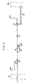
- Fig. 2 shows a circuit diagram of the touch sensor means.
- an amplifying means such as a complementary metal oxide semiconductor (CMOS) G1 and is rectifyed by a circuit including diodes D1 and D2, a resistor R2 and a condenser C1.
- CMOS complementary metal oxide semiconductor
- the signal level exceeds a threshold votage level, an output level of the CMOS becomes lowered and light emitting element 4 such as a LED emits a light beam.
- the light emitting element does not work when an operator does not touch the sensor means 3 at sensor electrode 1 since a high level of voltage is incurred to the input of CMOS G1 and both the output level of the CMOS G1 and an input level of CMOS G2 are equally lowered resulting in a high level of the latter CMOS G2.
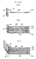
- terminals 9 at one end of lead wires 8 are inserted into cavities 7 of the connector housing B1 in an order as shown in Fig. 3(A) and (B).
- any one among terminals 9 may be arbitrarily inserted into one of the cavities 7 of the connector housing B1.
- the connector housing B1 is engaged with the connector housing A1 and terminals 9 are thus connected with the other end of the lead wires 8 function as the sensor electrode (as shown in Fig 3 (C)).
- the connector housing B2 is engaged with the connector housing A2 and a cavity 11 [11a, 11b,...11n] of the connector housing B2 is connected with cavitiy 6 of connector housing A2 respectively (as shown in Fig. 3 (D)).
Landscapes
- Engineering & Computer Science (AREA)
- Manufacturing & Machinery (AREA)
- Microelectronics & Electronic Packaging (AREA)
- Details Of Connecting Devices For Male And Female Coupling (AREA)
Description
- The present invention relates to an improved device and method of identifying a cavity in a housing of an electrical connector into which a terminal attached to an electric wire shall be inserted.
- The method of, and the device for identifying and indicating the specific cavity in a connector housing of the present invention is particularly useful when a plurarity of wires share a single connector housing with equivalent number of cavities to the number of wires, and when the wire terminal is connected with the mating connector terminal by manualIy inserting the wire with terminal into the corresponding cavity of the connector housing.
- Up to now, in order to connect the terminal placed in one end of the lead wire with the connector housing, an operator puts the terminal into the cavity in a way that when he watches the cavity in a direction of the terminal's insertion, the cavity is allotted a number beginning from the left end to the right end in the first row and is given a number from the left end to the right end in the second row and those numbers and colours of the insulation coating of the lead wire are correlated. In the ahove mentioned connecting method it is diffcult for an operator, especially for a beginner, to put the terminal into the correct cavity according to instructions of those indices of colour and number. Particularly when the assembling wire is little in quantity and large in species, it is difficult for him to put the terminal into the right cavity in the housing because soon after he has become familiar with how to put the terminal into the corresponding cavity, he must learn another rule for putting the terminal into the cavity from the beginning.
- DE-A-20 25 357 shows a method and an apparatus for identifying locations of electrical components with respect to a housing or the like. There is provided a kind of tool, by means of said tool one of a plurality of wires must be gripped in order to have a closed circuit such that one of a plurality of light emitting elements emits light into a corresponding lightwave guide which in turn indicates the correct position the wire must be inserted. So, it is necessary for an operator to positively grip one of the lead wires with the tool, because otherwise there is no closed electrical loop between tool, lead wire and the respective light emitting element lying in series therewith.
- So, it is an object of the present invention to provide a method of identifying cavity locations of an electrical connector and an indication device for the same making it possible to positively identify the cavity in which a terminal has to be inserted without the necessity of tools or the like.
- Solution of this object is achieved by what is claimed in
claim - According to the present invention, it is only necessary to grip one of the respective terminals to be inserted in a connector cavity by hand and by means of a simple touch or grip of the respective terminal by the operator's hand the connector cavity associated to said terminal is illuminated. Accordingly, detection of the correct cavity and a subsequent easy insertion of the terminal into the connector cavity is possible without the necessity of additional tools or the like.
- According to the method of the present invention, the specific cavity in the second connector in a harness, to which the cavity of the first connector in the same harness corresponds, is identically indicated by illuminating the cavity with a light emitting diode equipped in a cavity of the mating connector.The LED emits light beams when a wiring operator touches a terminal which should be inserted for connection into the cavity in the second connector in a harness. The indication device for identifying the corresponding cavity is composed of connector housings with cavities, touch sensor means located inbetween the housings, a LED and a light wave guide. The touch sensor works when it catches the low pitched composite tone (hum) at the receiver output caused by fluctuations in the power supply induced by the human body.
- The following is a more detailed description of the present invention taken in conjunction with the accompanying drawings in which:
- Fig. 1
- is a schematic diagram showing the method of identifying cavities in a housing of an electrical connector of the present invention;
- Fig. 2
- illustrates an electrical circuit for indication of a specific cavity in a housing of an electrical connector used in the present invention; and
- Figs. 3(A) to 3(F)
- illustrate the process for assemblying a plurality of electric wire leads according to the method of the present invention.
- In the following description as well as in the claims, a single reference numeral always denotes a plurality of identical components or elements. This is furthermore emphazised by listing the sub-numerals having indices from "a" to "n" upon the first appearance of each reference numeral in the following description.
- According to Figs 1 to 3(A), electrical terminals 9 [9a, 9b,...9n] and 10 [1Oa, 10b,...1On] are connected at the respective ends of lead wires 8 [8a, 8b,.. .8n]. The terminals 9 are inserted into cavities 7 [7a, 7b,...7n] in a connector housing B1.
- Referring to Fig. 1, the method of identifying cavity locations in a housing of electrical connector is described. In the figure a circuit in the middle is the identification circuit of the present invention including two connectors A1 and A2 both having a plurality of open cavities 2 [2a, 2b,...2n) and 6 [6a, 6b,...6n], respectively. Between the two connectors A1 and A2 there are located a power source, touch sensor means 3 [3a, 3b,...3n], light emitting diodes 4 [4a, 4b,...4n] whose emitted light beams are transmitted by optical fibers 5 [5a, 5b,...5n] into the
cavities 6 of the second connector A2. The first connector A1 in practice is placed in an engagement with the connector B1. Electrically connected with the second connector A2 there is a connector B2 without wire lead. The touch sensor means 3 is designed in a way that it detects the hum in the power source of the indication circuit and the light emitting elements 4 such as a light emitting diode (LED) emit a light beam when an operator in the practice touches any of the terminals 10 attached to the open ends of wire leads 8. The emitted light beam is introduced into the correspondingopen cavity 6 in the second connector housing A2 through which the light beam can be visually recognized in the frame of the facing cavity 11 in the mated connector B2 and thus the location of the desired cavity 11 which corresponds thereto and thus an accurate connecting is made by merely inserting the electrical terminal 10 into the indicated cavity 11 in eletrical connector B2. - Fig. 2 shows a circuit diagram of the touch sensor means. When an operator touches sensing electrode 1 [1a, 1b,...1n] in the sensor means 3, a human body which works as an antenna causes a hum in the power source and the signal is inverted and amplified by an amplifying means such as a complementary metal oxide semiconductor (CMOS) G1 and is rectifyed by a circuit including diodes D1 and D2, a resistor R2 and a condenser C1. When the signal level exceeds a threshold votage level, an output level of the CMOS becomes lowered and light emitting element 4 such as a LED emits a light beam. On the contrary the light emitting element does not work when an operator does not touch the sensor means 3 at
sensor electrode 1 since a high level of voltage is incurred to the input of CMOS G1 and both the output level of the CMOS G1 and an input level of CMOS G2 are equally lowered resulting in a high level of the latter CMOS G2. - Referring now to Figs. 3(A) to 3(F), terminals 9 at one end of lead wires 8 are inserted into
cavities 7 of the connector housing B1 in an order as shown in Fig. 3(A) and (B). When all circuits including lead wires 8 are of the same electric potential and when each lead wire 8 has the same electrical capacity, any one among terminals 9 may be arbitrarily inserted into one of thecavities 7 of the connector housing B1. The connector housing B1 is engaged with the connector housing A1 and terminals 9 are thus connected with the other end of the lead wires 8 function as the sensor electrode (as shown in Fig 3 (C)). When the above mentioned process is carried out, the connector housing B2 is engaged with the connector housing A2 and a cavity 11 [11a, 11b,...11n] of the connector housing B2 is connected withcavitiy 6 of connector housing A2 respectively (as shown in Fig. 3 (D)). - When the operator selects and holds terminals 10 which are provided at the other end of the plurality of lead wires 8 and touch sensor means 3 work, light emitting elements 4 located in
cavities 6 of the connector housing A2 will indicate one of the cavities 11 of the connector housing B2 connected withcavities 6. By watching illuminated cavity 11, the operator puts terminals 10 into the corresponding cavity 11 (as shown in Fig. 3(E)). When the above mentioned work is completed, connector housings B1 and B2 are taken off connector housings A1 and B1. The assembly of electric wires which includes connector housings at both ends is completed (as shown in Fig. 3 (F)). - When any modification of the electrical circuit design must be made, mere shifting of the light transmittion guide(s) 5 to the newly destined cavity location(s) is sufficient for assembly practices.
- Finally, the following is a list of reference numerals used in the foregoing description and the accompanying claims:
- 1 [1a, 1b,...1n]
- sensor contact point
- 2 [2a, 2b,...2n]
- cavity
- 3 [3a, 3b,...3n]
- touch sensor means
- 4 [4a, 4b,...4n]
- light emitting element
- 5 [5a, 5b,...5n]
- light wave guide
- 6 [6a, 6b,...6n]
- cavity
- 7 [7a, 7b,...7n]
- cavity
- 8 [8a, 8b,...8n]
- lead wire
- 9 [9a, 9b,...9n]
- terminal
- 10 [10a, 10b,...10n]
- terminal
- 11 [11a, 11b,...11n]
- cavity
- A1, A2, B1 and B2
- connector housing
Claims (2)
- A device for indicating a cavity location in the housing of an electrical connector (B2) and intended for use in making connections between two electrical connectors (B1, B2), comprising the following elements:
a first connector housing (A1) with cavities (2), electrically connected with a sensor means (3) and being capable to be mated with one (B1) of said electrical connectors (B1, B2), which is itself connected to the wires (8) of a cable;
a light emitting element (4) connected to said sensor means (3) which emits a light beam or not, depending on the level of the output of said sensor means;
a light wave guide (5) for transmitting the light beam being emitted by said light emitting element (4); and
a second connector housing (A2) with open cavities (6), which receive an end portion of said light wave guide (5) and are free from obstacles for passage of a light beam, said second connector housing (A2) being capable to be mated with the other electrical connector (B2) before said other electrical connector (B2) receives the other end of said wires (8) of said cable,
characterized in that
said sensor means (3) is comprised of a touch sensor means being sensitive for the touch of a human person for detecting a hum in a power source of said device, said touch sensor means consisting substantially of switching elements (G1, G2), a power supply, resistors (R1, R2), an amplifier rectifyer (R2, D1, D2), a condenser (C1) and input/output-terminals (1, Vcc). - A method of making a connection between two electrical connectors (B1, B2) with wire leads (8) including the steps of:- connecting each terminal (9) attached to one end portion of each wire lead (8) with a mating connector terminal in a cavity (7) of one (B1) of the electrical connectors (B1, B2), thereby leaving the other end portion (10) of each wire lead (8) unconnected;- connecting a touch sensor means (3) which is capable of detecting a hum at an electric power source with the connector terminal in each of the cavities (7) of said first electrical connector (B1) and with a light emitting element (4) with a light wave guide (5) for transmission of a light beam upon occurence of detection of a hum, said touch sensor means consisting essentially of switching elements (G1, G2), a power supply, resistors (R1, R2), an amplifier rectifyer (R2, D1, D2), a condenser (C1) and input/output-terminals (1, Vcc);- introducing the end portion of the light wave guide (5) into an open cavity of an electrical connector (A2) to be mated with said second electrical connector (B2) having no obstacle for passage of the light beam; and- allowing illumination of a specific cavity (11) in the second electrical connector (B2) through the facing cavity (6) in said electrical connector (A2) by light beams, by touching one of the open ends (10) of the wire leads (8), and thus indicating location of the corresponding cavity (11) into which the terminal (10) on the wire lead (8) is to be be inserted and connected.
Applications Claiming Priority (2)
| Application Number | Priority Date | Filing Date | Title |
|---|---|---|---|
| JP61097548A JPS62254316A (en) | 1986-04-25 | 1986-04-25 | Supplementary apparatus for assembly of wiring harness containing connectors and application of the same |
| JP97548/86 | 1986-04-25 |
Publications (3)
| Publication Number | Publication Date |
|---|---|
| EP0242876A2 EP0242876A2 (en) | 1987-10-28 |
| EP0242876A3 EP0242876A3 (en) | 1989-04-26 |
| EP0242876B1 true EP0242876B1 (en) | 1992-08-12 |
Family
ID=14195293
Family Applications (1)
| Application Number | Title | Priority Date | Filing Date |
|---|---|---|---|
| EP19870105922 Expired EP0242876B1 (en) | 1986-04-25 | 1987-04-23 | Method of indentifying cavity locations of electrical connector and indication device for the same |
Country Status (5)
| Country | Link |
|---|---|
| EP (1) | EP0242876B1 (en) |
| JP (1) | JPS62254316A (en) |
| CA (1) | CA1307921C (en) |
| DE (1) | DE3781006T2 (en) |
| ES (1) | ES2033717T3 (en) |
Families Citing this family (7)
| Publication number | Priority date | Publication date | Assignee | Title |
|---|---|---|---|---|
| JPH0831289B2 (en) * | 1986-10-13 | 1996-03-27 | 住友電装株式会社 | Terminal insertion guide device for harness assembly |
| GB8925001D0 (en) * | 1989-11-06 | 1989-12-28 | Molex Inc | Apparatus for assembling terminated wires into connectors to form electrical harnesses |
| JP3009124B2 (en) * | 1994-09-26 | 2000-02-14 | 矢崎総業株式会社 | Terminal insertion guidance device |
| JP3008806B2 (en) * | 1995-03-23 | 2000-02-14 | 住友電装株式会社 | Inspection device for connector wire arrangement indication |
| US6793401B2 (en) | 2002-08-22 | 2004-09-21 | The Boeing Company | System and method for assembling a bundle of conductors into a connector |
| DE102016109464B4 (en) * | 2016-05-24 | 2024-09-26 | Lisa Dräxlmaier GmbH | Optical assembly display for cable harnesses |
| FR3053472B1 (en) * | 2016-06-29 | 2018-08-10 | Alstom Transport Technologies | DEVICE FOR ASSISTING REPLACEMENT OF A FIRST CONNECTOR WITH A SECOND CONNECTOR AND METHOD FOR REPLACING ASSISTANCE |
Family Cites Families (2)
| Publication number | Priority date | Publication date | Assignee | Title |
|---|---|---|---|---|
| FR2060486A5 (en) * | 1969-09-22 | 1971-06-18 | Epe Corp | |
| US4462155A (en) * | 1982-04-01 | 1984-07-31 | Combustion Engineering, Inc. | Pin locator |
-
1986
- 1986-04-25 JP JP61097548A patent/JPS62254316A/en active Pending
-
1987
- 1987-04-23 ES ES87105922T patent/ES2033717T3/en not_active Expired - Lifetime
- 1987-04-23 EP EP19870105922 patent/EP0242876B1/en not_active Expired
- 1987-04-23 DE DE19873781006 patent/DE3781006T2/en not_active Expired - Fee Related
- 1987-04-24 CA CA000535490A patent/CA1307921C/en not_active Expired - Fee Related
Also Published As
| Publication number | Publication date |
|---|---|
| DE3781006T2 (en) | 1993-01-14 |
| ES2033717T3 (en) | 1993-04-01 |
| EP0242876A2 (en) | 1987-10-28 |
| DE3781006D1 (en) | 1992-09-17 |
| EP0242876A3 (en) | 1989-04-26 |
| CA1307921C (en) | 1992-09-29 |
| JPS62254316A (en) | 1987-11-06 |
Similar Documents
| Publication | Publication Date | Title |
|---|---|---|
| US4767168A (en) | Hybrid connector cable system | |
| US4720630A (en) | Active optical connector including an electronic circuit board and an optical fiber | |
| US5062807A (en) | Lighted electrical connector permitting multi directional viewing | |
| US6095851A (en) | Status indicator for electronic device | |
| US5244409A (en) | Molded connector with embedded indicators | |
| EP0079106B1 (en) | Fiber optic connector | |
| US5345520A (en) | Electrical connector with an optical fiber connection detector | |
| US20050032415A1 (en) | Connector component and connector assembly | |
| US4950169A (en) | Universal cable connector for electronic devices | |
| JPH10507297A (en) | Programmable cable adapter | |
| WO2007109460A2 (en) | Method for distinguishing a first group of wires from other wires of a multi-wire cable, test connector for use in this method and a kit comprising such a multiwire cable and test connector | |
| JPS63226608A (en) | Optical connector | |
| EP0242876A2 (en) | Method of indentifying cavity locations of electrical connector and indication device for the same | |
| US4698585A (en) | Apparatus for identifying the connection position of a wire having two modes of operation | |
| US7127041B1 (en) | Simultaneous tracing of multiple phone/data cables | |
| CN114114082A (en) | Jumper Identification Inspection System | |
| JP3321564B2 (en) | Photoelectric shared transmission device, holder and equipment | |
| JPH11214100A (en) | Composite connector device for optical signal and power | |
| JPH08211256A (en) | Optical module, optical connector and composite module | |
| JP2000340312A (en) | Signal transmission device and plug | |
| JP3215685B2 (en) | Plug / jack type shared optical transmission device and optical fiber plug | |
| JPH0421277Y2 (en) | ||
| JPH04155874A (en) | Optical output control system | |
| JPH0581003B2 (en) | ||
| JP3357873B2 (en) | Fiber optic cable and audio or information equipment |
Legal Events
| Date | Code | Title | Description |
|---|---|---|---|
| PUAI | Public reference made under article 153(3) epc to a published international application that has entered the european phase |
Free format text: ORIGINAL CODE: 0009012 |
|
| AK | Designated contracting states |
Kind code of ref document: A2 Designated state(s): DE ES FR GB |
|
| PUAL | Search report despatched |
Free format text: ORIGINAL CODE: 0009013 |
|
| AK | Designated contracting states |
Kind code of ref document: A3 Designated state(s): DE ES FR GB |
|
| 17P | Request for examination filed |
Effective date: 19891024 |
|
| 17Q | First examination report despatched |
Effective date: 19910128 |
|
| GRAA | (expected) grant |
Free format text: ORIGINAL CODE: 0009210 |
|
| AK | Designated contracting states |
Kind code of ref document: B1 Designated state(s): DE ES FR GB |
|
| REF | Corresponds to: |
Ref document number: 3781006 Country of ref document: DE Date of ref document: 19920917 |
|
| ET | Fr: translation filed | ||
| REG | Reference to a national code |
Ref country code: ES Ref legal event code: FG2A Ref document number: 2033717 Country of ref document: ES Kind code of ref document: T3 |
|
| PLBE | No opposition filed within time limit |
Free format text: ORIGINAL CODE: 0009261 |
|
| STAA | Information on the status of an ep patent application or granted ep patent |
Free format text: STATUS: NO OPPOSITION FILED WITHIN TIME LIMIT |
|
| 26N | No opposition filed | ||
| PGFP | Annual fee paid to national office [announced via postgrant information from national office to epo] |
Ref country code: FR Payment date: 20010409 Year of fee payment: 15 |
|
| PGFP | Annual fee paid to national office [announced via postgrant information from national office to epo] |
Ref country code: GB Payment date: 20010418 Year of fee payment: 15 Ref country code: DE Payment date: 20010418 Year of fee payment: 15 |
|
| PGFP | Annual fee paid to national office [announced via postgrant information from national office to epo] |
Ref country code: ES Payment date: 20010430 Year of fee payment: 15 |
|
| REG | Reference to a national code |
Ref country code: GB Ref legal event code: IF02 |
|
| PG25 | Lapsed in a contracting state [announced via postgrant information from national office to epo] |
Ref country code: GB Free format text: LAPSE BECAUSE OF NON-PAYMENT OF DUE FEES Effective date: 20020423 |
|
| PG25 | Lapsed in a contracting state [announced via postgrant information from national office to epo] |
Ref country code: ES Free format text: LAPSE BECAUSE OF NON-PAYMENT OF DUE FEES Effective date: 20020424 |
|
| PG25 | Lapsed in a contracting state [announced via postgrant information from national office to epo] |
Ref country code: DE Free format text: LAPSE BECAUSE OF NON-PAYMENT OF DUE FEES Effective date: 20021101 |
|
| GBPC | Gb: european patent ceased through non-payment of renewal fee |
Effective date: 20020423 |
|
| PG25 | Lapsed in a contracting state [announced via postgrant information from national office to epo] |
Ref country code: FR Free format text: LAPSE BECAUSE OF NON-PAYMENT OF DUE FEES Effective date: 20021231 |
|
| REG | Reference to a national code |
Ref country code: FR Ref legal event code: ST |
|
| REG | Reference to a national code |
Ref country code: ES Ref legal event code: FD2A Effective date: 20030514 |