EP0240580B1 - Three-stage coupling arrangement - Google Patents
Three-stage coupling arrangement Download PDFInfo
- Publication number
- EP0240580B1 EP0240580B1 EP86104544A EP86104544A EP0240580B1 EP 0240580 B1 EP0240580 B1 EP 0240580B1 EP 86104544 A EP86104544 A EP 86104544A EP 86104544 A EP86104544 A EP 86104544A EP 0240580 B1 EP0240580 B1 EP 0240580B1
- Authority
- EP
- European Patent Office
- Prior art keywords
- switching
- outputs
- inputs
- stage
- array
- Prior art date
- Legal status (The legal status is an assumption and is not a legal conclusion. Google has not performed a legal analysis and makes no representation as to the accuracy of the status listed.)
- Expired - Lifetime
Links
Images


Classifications
-
- H—ELECTRICITY
- H04—ELECTRIC COMMUNICATION TECHNIQUE
- H04Q—SELECTING
- H04Q3/00—Selecting arrangements
- H04Q3/64—Distributing or queueing
- H04Q3/68—Grouping or interlacing selector groups or stages
-
- H—ELECTRICITY
- H05—ELECTRIC TECHNIQUES NOT OTHERWISE PROVIDED FOR
- H05K—PRINTED CIRCUITS; CASINGS OR CONSTRUCTIONAL DETAILS OF ELECTRIC APPARATUS; MANUFACTURE OF ASSEMBLAGES OF ELECTRICAL COMPONENTS
- H05K7/00—Constructional details common to different types of electric apparatus
- H05K7/14—Mounting supporting structure in casing or on frame or rack
- H05K7/1438—Back panels or connecting means therefor; Terminals; Coding means to avoid wrong insertion
- H05K7/1459—Circuit configuration, e.g. routing signals
-
- H—ELECTRICITY
- H05—ELECTRIC TECHNIQUES NOT OTHERWISE PROVIDED FOR
- H05K—PRINTED CIRCUITS; CASINGS OR CONSTRUCTIONAL DETAILS OF ELECTRIC APPARATUS; MANUFACTURE OF ASSEMBLAGES OF ELECTRICAL COMPONENTS
- H05K2201/00—Indexing scheme relating to printed circuits covered by H05K1/00
- H05K2201/09—Shape and layout
- H05K2201/09209—Shape and layout details of conductors
- H05K2201/09218—Conductive traces
- H05K2201/09236—Parallel layout
-
- H—ELECTRICITY
- H05—ELECTRIC TECHNIQUES NOT OTHERWISE PROVIDED FOR
- H05K—PRINTED CIRCUITS; CASINGS OR CONSTRUCTIONAL DETAILS OF ELECTRIC APPARATUS; MANUFACTURE OF ASSEMBLAGES OF ELECTRICAL COMPONENTS
- H05K2201/00—Indexing scheme relating to printed circuits covered by H05K1/00
- H05K2201/09—Shape and layout
- H05K2201/09209—Shape and layout details of conductors
- H05K2201/09218—Conductive traces
- H05K2201/09245—Crossing layout
-
- H—ELECTRICITY
- H05—ELECTRIC TECHNIQUES NOT OTHERWISE PROVIDED FOR
- H05K—PRINTED CIRCUITS; CASINGS OR CONSTRUCTIONAL DETAILS OF ELECTRIC APPARATUS; MANUFACTURE OF ASSEMBLAGES OF ELECTRICAL COMPONENTS
- H05K2201/00—Indexing scheme relating to printed circuits covered by H05K1/00
- H05K2201/09—Shape and layout
- H05K2201/09209—Shape and layout details of conductors
- H05K2201/09218—Conductive traces
- H05K2201/09272—Layout details of angles or corners
Definitions
- the invention relates to a three-stage coupling arrangement in multiple space technology for electrical communication technology according to the preamble of claim 1.
- Coupling arrangements are used to selectively connect signal sources to signal sinks. There are single and multi-stage coupling arrangements.
- a three-stage coupling arrangement is from FIG. 2 and the associated text of the essay by Charles Clos: "A Study of Non-Blocking Switching Networks” on pages 406 to 424 of the US magazine: “The Bell System Technical Journal”, Volume XXXII, Known in 1953.
- the coupling arrangement shown there in FIG. 2 has a first stage, stage (a), a second stage, stage (b), and a third stage, stage (c).
- Each stage is made up of several coupling matrices.
- the coupling matrices of one stage differ in the number of their inputs and outputs from those of the other stages: For example, those of the first stage have 6 inputs and 11 outputs, those of the second stage 6 inputs and 6 outputs and those of the third stage 11 inputs and 6 Outputs on. So three different designs of coupling matrices are required.
- the number of versions is reduced to two if switching means are used for the crosspoints that enable signal transmission in both directions, e.g. is the case with metallic contacts.
- the version intended for the first stage can then also be used in the third stage, with the inputs and outputs being interchanged.
- the invention has for its object to provide a coupling arrangement of the type mentioned above, in which the coupling matrices of all stages are constructed identically.
- FIG. 1 represents a block diagram of the coupling arrangement according to the invention.
- the coupling arrangement consists of a first and a second, identical switching matrix KF1 or KF2.
- Each switching matrix consists of a first, a second and a third stage M1, M2 or M3, that is to say has three stages.
- Each stage contains 16 similar coupling matrices G1. to G16, each with 16 inputs and 16 outputs.
- Each input of a switching matrix of the first stage forms an input of the switching matrix concerned.
- 16 coupling matrices G1 to G16 each with 16 inputs, 256 inputs E001 to E256 of the switching matrix KF1 or KF2 result.
- the outputs of the coupling matrices of the third stage form the 256 outputs A001 to A256.
- a first parallel wiring P1 connects each of the inputs E001 to E256 of the first switching matrix KF1 to the input of the same name of the second switching matrix.
- the outputs A001 to A256 are connected via a second parallel wiring P2.
- the two switching networks KF1 and KF2 are connected in parallel.
- FIG. 2 represents a block diagram of the first and second switching matrix KF1 and KF2.
- the first, second and third stages M1, M2 and M3 and the coupling matrices G1 to G16 are shown again.
- Each coupling matrix consists of 256 coupling points KP arranged in a 16x16 matrix.
- the inputs E1 to E16 and the outputs A1 to A16 of each coupling matrix are also specified.
- connections specified under a) and b) also apply mutatis mutandis to the intermediate line routing between the second and third stages.
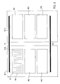
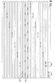
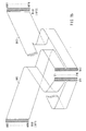
- FIG. 3 There are two cabinets, one for each switching matrix. In order to clarify this assignment, the cabinets were designated with the corresponding reference numbers KF1 and KF2 of the coupling fields. Each cabinet contains a first, a second and a third magazine M1, M2 and M3. Each magazine contains the 16 coupling matrices G1 to G16 of one level. The respective assignment is indicated by the identical reference symbols M1, M2 and M3 for the magazines on the one hand and the stages in FIGS. 1 and 2.
- Each coupling matrix is designed as a plug-in module. Since each stage comprises 16 coupling matrices according to FIGS. 1 or 2, each magazine also contains 16 plug-in modules. These 16 plug-in modules are shown in the first magazine M1 of the first cabinet KF1, the first being designated G1 and the last G16. By selecting the same reference numerals G1 to G16, the assignment to the coupling matrices shown in FIGS. 1 and 2 is again indicated. The first and second parallel cabling were designated P1 and P2.
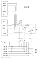
- the control of the two switching matrixes KF1 and KF2 by a common control unit St is shown on the basis of FIG.
- This control has four outputs for the addresses characterizing the crosspoint to be switched through, namely for the column address Sp.-A, for the row address Z.-A. and for the coupling matrix address Km.-A. as well as two outputs for the stage address St.-A., on.
- These outputs are connected via four or two wires to the inputs of the same name on the Koppelfeler KF1 and KF2. Since each switching matrix has 16 columns and 16 rows, each step contains 16 switching matrices and each switching matrix has 3 steps, each using four bits is sufficient for the unambiguous identification of a switching point to be switched through.
- Each of the coupling fields KF1 and KF2 alone enables a connection of each input to any output.
- blockages can occur, i.e. if there are already several connections, another connection leading from a specific input to a specific output can no longer be switched through. These blockages are avoided by the parallel connection of two such switching networks according to the invention, so that the coupling arrangement according to the invention is therefore free of blocking.
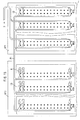
- the first magazine M1 is located at the top, below that is the second magazine M2 and at the bottom the third magazine M3. They are mechanically connected to one another in a manner not shown. The second magazine is therefore adjacent to both the first and the third.
- Each magazine has 16 guide strips F at the top and bottom, into which the plug-in modules are guided. Only the lower guide bars are visible. Of the 48 plug-in modules (16 per magazine), only the sixteenth plug-in module G16 of the third magazine M3 is shown.
- Each plug-in module carries a first and a second plug strip S1 or S2 as plug connectors. Instead of the two connector strips S1 and S2, a single, large connector strip can also be provided.
- first and a second backplane circuit board L1 and L2 are shown. Each carries two rows of 16 socket strips as mating connectors, with socket strips B1 to B16 forming the upper row and socket strips B17 to B32 forming the lower row. The socket strip B17 and some other socket strips, not shown, are not visible here.
- a third and a fourth backplane L3 and L4 are also provided. These only carry a row of 16 socket strips B33 to B48 or B49 to B64.
- Dashed lines indicate in which of the guide strips the plug-in module G16 shown is inserted when it is plugged in, the position of the backplane on the back of the magazine after assembly and that the plug-in strips S1 and S2 of the plug-in module G16 shown in the socket strip B32 of the second Engage the backplane L2 and the female connector B64 of the fourth backplane L4.
- the plug strips of the plug-in modules, not shown engage in the socket strips assigned to them. This results in an assignment according to the following table: If, instead of the two plug strips S1 and S2, a single large plug strip is provided, the respective part engages in the corresponding socket strip according to the table above.
- the backplane circuit board L1 thus comprises the area of the connector strips S2 of the first magazine M1 and the area of the connector strips S1 of the second magazine M2.
- the area of the connector strips S2 of the first magazine M1 is adjacent to the area of the connector strips S1 of the second magazine M2. The same applies analogously to the backplane L2.
- FIG. 6 shows one of the plug-in modules G1 to G16. It consists of a printed circuit board LP, which carries the 256 coupling points KP arranged in a 16x16 matrix, a first connector strip S1 and a second connector strip S2.
- the printed circuit board LP has conductor tracks LB which connect the coupling points KP to one another and to the 16 inputs E1 to E16 and the 16 outputs A1 to A16 on the connector strips S1 and S2.
- the inputs E1 to E16 are all on the first connector S1, the outputs A1 to A16 are all led out on the second connector S2.
- the first connector strip S1 is closest to the first magazine M1.
- the inputs E1 to E16 are brought out on it, because according to FIG. 2 they have to be connected to the outputs of the plug-in modules of the first magazine M1.
- the conductor tracks LB were shown here as single-pole. However, since switching matrixes are usually made with two or even four wires, you have to imagine two or four conductor tracks instead of a line and a corresponding number of connector pins on the connector strips.
- FIGS. 7, 8 and 9 show one of the backplane circuit boards L1 and L2. Place these figures next to each other, Figure 7 on the left and Figure 9 on the right.
- the respective upper and lower lines as well as the left and right lines on FIGS. 7 and 9 indicate the outlines of this backplane.
- B1 to B16 (top row) and B17 to B32 denote the locations for the socket strips B1 to B32. These socket strips themselves are not shown, but only the pads for their soldering pins are indicated by dots. If one looks at the first backplane L1, as can be seen from FIGS. 5 and 6, the outputs A1 to A16 of the plug-in modules G1 to G16 from the first magazine M1 lie on the socket strips B1 to B16.
- the inputs E1 to E16 of the plug-in modules of the second magazine M2 are located on the socket strips B17 to B32, starting at the top with E1 and A1.
- the intermediate lines which are to be created according to FIG. 2 are formed by conductor tracks LB '.
- a single-pole display was chosen here again; and one has to imagine two conductor tracks instead of a line, since, as can be seen from the illustration of two solder eyes for each input and output, here a backplane for a two-wire switching matrix is drawn. Only a few of the many intermediate lines are shown here. In addition, it is not shown that the conductor tracks are distributed over different levels of a multilayer board in order to accommodate their large number and to be able to cross them.
- the second backplane is designed like the first, since, according to FIG. 2, the system of the intermediate line routing between the first and the second stage is the same as that between the second and third stages.
- the 256 inputs E001 to E256 are on the socket strips B33 to B48 of the third backplane L3 and the outputs A001 to A256 of the respective switching matrix KF1 or KF2 are on the socket strips B49 to B64 of the fourth backplane L4.
- the parallel wiring P1 and P2 as well as the connections to the signal sources Q and the signal sinks S are connected to the solder pins of these socket strips.
- Switching means and control lines for switching the switching points on and off are not shown. This also applies to the plug-in modules.
- the development according to claim 3 ensures that the coupling arrangement according to the invention is suitable for the transmission of digital signals with a bit rate of up to 150 Mbit / s.
- FIG. 10 shows a section through such a backplane to show the position of the conductor tracks in it. It has 19 layers, between which the hatched conductor tracks lie.
- a two-wire switching matrix is assumed, i.e. each connection is designed as a pair of conductor tracks. The first pair is labeled LB1 and lies on the first level between the first and second layers.
- the second pair LB2 is not arranged directly next to the first pair LB1 in the next, that is to say the second level, but is laterally offset in accordance with the crosstalk attenuation requirement.
- This transfer extends over eight levels.
- the ninth and tenth levels carry the conductor tracks StL for the control lines not shown in FIGS. 7 to 9.
- the given crosstalk attenuation requirements only allow a pair LB3 to be arranged again in the eleventh level without displacement relative to the first pair LB1.
- the signal sources Q are connected to the inputs E001 to E256 without reflection. How this is achieved will be explained with reference to FIG. 11.
- the two cabinets or coupling fields KF1 and KF2 and the backplane L3 located in them are indicated.
- the dots represent the soldering pins of the socket strips B33 to B48.
- a cable that is not labeled leads from the signal sources Q to the socket strips B33 to B48 in the first cabinet KF1, and the wires from this cable are soldered to the soldering pins of these socket strips. Only a few of these wires are shown.
- the wires of the parallel wiring P1 are also soldered to these soldering pins.
- Resistors R are also connected to these solder pins. Their resistance value is chosen equal to the characteristic impedance of the parallel cabling P1 and the cable coming from the signal sources Q. These resistors bring about the required reflection-free termination, since the coupling matrices themselves cannot offer such a termination because of their high input resistance. Instead of soldering, any other connection technology can also be used.
- the resistors R and the cable coming from the signal sources can also be interchanged, ie the cable ends in the second cabinet KF2 and the resistors R are in the first cabinet KF1.
- the corresponding design of the "parallel cabling" on the output side is described with reference to FIG.
- the two cabinets KF1 and KF2 with their 256 outputs A001 to A256 and 256 electronic changeover switches U001 to U256 are indicated.
- Each of the outputs A001 to A256 is connected to the associated first or second input of the associated electronic switch U001 to U256.
- the outputs of the electronic changeover switches are connected to the signal sinks S.
- the electronic changeover switches also have control inputs which are controlled by a changeover control U.-St. are connected. This changeover control can thus control the electronic changeover switch into its first or second switching position.
- the first switching position is drawn, in which the respective output of the first switching matrix KF1 is switched through to the relevant signal sink S.
- the coupling matrices G1 to G16 already have terminating resistors on the output side, a simple parallel connection on the output side is not possible, as is the case with the inputs. Rather, only one of the relevant outputs of the switching networks KF1 or KF2 may be switched through to the relevant signal sink S. This is caused by the electronic changeover switches U001 to U256, depending on whether the respective connection was switched through via the first switching matrix KF1 or via the second switching matrix KF2.
- the switching control U.-St. from the column address Sp.-A., the row address Z.-A., the coupling matrix address Km.-A., the step addresses St.-A. and the cabinet addresses Schr.-A.1 and Schr.-A.2. It is therefore connected to the corresponding outputs of the control unit St already mentioned in the description of FIG.
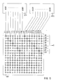
- FIG. 13 An advantageous embodiment of the electronic changeover switch is described with reference to FIG. 13.
- the same coupling matrices are used as electronic changeover switches as are used in the coupling fields KF1 and KF2 and are described with reference to FIG. 6.
- Such a coupling matrix is also shown in FIG. 13 and labeled GU1 there.
- the 256 crosspoints are indicated by circles.
- the inputs E1 to E8 are connected to the outputs A001 to A008 of the first switching matrix KF1.
- the inputs E9 to E16 are connected to the outputs A001 to A008 of the second switching matrix KF2.
- the associated 8 signal sinks S are connected to the outputs A1 to A8 of this coupling matrix.
- the function is as follows: a connection to the signal sink connected to the output A1 of the coupling matrix GU1 is switched through, then in this coupling matrix either the coupling point connecting the input E1 or the input E9 with the output A1 is switched through, depending on whether the connection is via the first or the second Coupling field KF1 or KF2 is performed. The same procedure is followed when establishing a connection to the other outputs.
- the coupling points required for this are highlighted in FIG. 13 by two circles.
- the other outputs A009 to A256 of switching matrixes KF1 and KF2 are interconnected in the same way. This results in 32 such coupling matrices. Your accommodation is described with reference to Figure 14.
- the two cabinets KF1 and KF2 also contain the fourth magazines M4, which hold the 32 coupling matrices GU1 to GU32.
- the coupling matrices GU1 to GU16 are in the first cabinet KF1, the coupling matrices GU17 to GU32 are in the second cabinet KF2.
- the outputs A001 to A016 of the first switching matrix KF1 are connected to the inputs E1 to E8 of the switching matrixes GU1 and GU2 via the first ribbon cable BK1.
- the outputs A001 to A016 of the second switching matrix KF2 are connected to the inputs E9 to E16 of the switching matrixes GU1 and GU2 via the second ribbon cable BK2.
- the ribbon cables are slotted longitudinally in the middle so that there are enough long ends for connection to the socket strips of the coupling matrices GU1 and GU2.
- the further outputs of the switching matrixes KF1 and KF2 are connected to the associated switching matrixes GU3 to GU32 via two ribbon cables.
- ribbon cables are made possible by the assignment of eight outputs of the coupling fields KF1 and KF2 to the inputs A1 to A8 or A9 to A16 of one of the coupling matrices GU1 to GU32 explained with reference to FIG. 13.
- the use of the ribbon cable ensures that these connections have electrical properties with little specimen scatter and are therefore suitable for the transmission of digital signals at a high bit rate.
Abstract
Description
Die Erfindung betrifft eine dreistufige Koppelanordnung in Raumvielfachtechnik für die elektrische Nachrichtenvermittlungstechnik nach dem Oberbegriff des Patentanspruches 1.The invention relates to a three-stage coupling arrangement in multiple space technology for electrical communication technology according to the preamble of
Koppelanordnungen werden verwendet, um Signalquellen wahlweise mit Signalsenken zu verbinden. Es gibt ein- und mehrstufige Koppelanordnungen. Eine dreistufige Koppelanordnung ist aus der Figur 2 und dem zugehörigen Text des Aufsatzes von Charles Clos: "A Study of Non-Blocking Switching Networks" auf den Seiten 406 bis 424 der US-Zeitschrift: "The Bell System Technical Journal ", Volume XXXII , 1953 bekannt.Coupling arrangements are used to selectively connect signal sources to signal sinks. There are single and multi-stage coupling arrangements. A three-stage coupling arrangement is from FIG. 2 and the associated text of the essay by Charles Clos: "A Study of Non-Blocking Switching Networks" on pages 406 to 424 of the US magazine: "The Bell System Technical Journal", Volume XXXII, Known in 1953.
Die dort in der Figur 2 abgebildete Koppelanordnung weist eine erste Stufe, stage (a), eine zweite Stufe, stage (b), und eine dritte Stufe, stage (c), auf. Jede Stufe ist aus mehreren Koppelmatrizen aufgebaut. Die Koppelmatrizen einer Stufe unterscheiden sich in der Anzahl ihrer Ein- und Ausgänge von denen der anderen Stufen: So weisen die der ersten Stufe 6 Eingänge und 11 Ausgänge, die der zweiten Stufe 6 Eingänge und 6 Ausgänge und die der dritten Stufe 11 Eingänge und 6 Ausgänge auf. Es sind also drei verschiedene Ausführungen von Koppelmatrizen erforderlich. Die Zahl der Ausführungen ermäßigt sich auf zwei, wenn man für die Koppelpunkte solche Schaltmittel verwendet, die eine Signalübertragung in beiden Richtungen ermöglichen, wie es z.B. bei metallischen Kontakten der Fall ist. Es kann dann die für die erste Stufe vorgesehene Ausführung unter Vertauschung der Ein- und Ausgänge auch in der dritten Stufe verwendet werden.The coupling arrangement shown there in FIG. 2 has a first stage, stage (a), a second stage, stage (b), and a third stage, stage (c). Each stage is made up of several coupling matrices. The coupling matrices of one stage differ in the number of their inputs and outputs from those of the other stages: For example, those of the first stage have 6 inputs and 11 outputs, those of the second stage 6 inputs and 6 outputs and those of the third stage 11 inputs and 6 Outputs on. So three different designs of coupling matrices are required. The number of versions is reduced to two if switching means are used for the crosspoints that enable signal transmission in both directions, e.g. is the case with metallic contacts. The version intended for the first stage can then also be used in the third stage, with the inputs and outputs being interchanged.
Diese Koppelanordnung ist blockierungsfrei. Das bedeutet, daß bei jeder möglichen Kombination von schon bestehenden Verbindungen zwischen je einer Signalquelle und je einer Signalsenke jede zusätzliche, allein aufgrund der noch freien Ein- und Ausgänge sinnvolle Verbindung auch tatsächlich durchgeschaltet werden kann. Dies gelingt, ohne daß das sogenannte "Umkoppeln", auch "Rearrangement" genannt, notwendig ist.This coupling arrangement is non-blocking. This means that with every possible combination of already existing connections between a signal source and a signal sink, each additional connection that is sensible solely because of the still free inputs and outputs can actually be switched through. This succeeds without the so-called "coupling", also called "rearrangement", being necessary.
Der Erfindung liegt die Aufgabe zugrunde, eine Koppelanordnung der oben genannten Art anzugeben, bei der die Koppelmatrizen aller Stufen gleich aufgebaut sind.The invention has for its object to provide a coupling arrangement of the type mentioned above, in which the coupling matrices of all stages are constructed identically.
Diese Aufgabe wird durch die kennzeichnenden Merkmale des Patentanspruches 1 gelöst.This object is achieved by the characterizing features of
In der Zeitschrift COMMUTATION ET ELECTRONIQUE, Nr. 49, April 1975, Seiten 23 bis 34, P. VOYER et al.: "Reseau de connexion pour grands centres temporeis" ist eine Koppelanordnung nach dem Zeitvielfachprinzip beschrieben. Aus der Figur 10 ist es an sich bekannt, Eingänge eines ersten Koppelfeldes mit den Eingängen eines zweiten Koppelfeldes und Ausgänge des ersten Koppelfeldes mit Ausgängen des zweiten Koppelfeldes zu verbinden.In the journal COMMUTATION ET ELECTRONIQUE, No. 49, April 1975, pages 23 to 34, P. VOYER et al .: "Reseau de connexion pour grands centers temporeis" describes a coupling arrangement according to the time division principle. It is known per se from FIG. 10 to connect inputs of a first switching matrix with the inputs of a second switching matrix and outputs of the first switching matrix with outputs of the second switching matrix.
Aus der Zeitschrift TELECOM REPORT, Band 6, Nr. 2, April 1983, Seiten 63 bis 68, B. SCHAFFER: "BIGFON-Vermittlungs- und Verteiltechnik", Bild 4c, ist ein dreistufiges Koppelfeld an sich bekannt, bei welchem jede Stufe die gleiche Zahl von Koppelmatrizen aufweist und wobei die Zahl der Eingänge einer jeden Koppelmatrix gleich der Zahl ihrer Ausgänge ist. Jedoch ist dieses Koppelfeld nicht blockierungsfrei.From the magazine TELECOM REPORT, Volume 6, No. 2, April 1983, pages 63 to 68, B. SCHAFFER: "BIGFON switching and distribution technology", Figure 4c, a three-stage switching network is known per se, in which each stage the has the same number of coupling matrices and the number of inputs of each coupling matrix is equal to the number of its outputs. However, this switching matrix is not free of obstructions.
Aus der DE-A-2 500 939 ist es an sich bekannt, für eine aus mehreren Baugruppen bestehende Koppelanordnung eine gemeinsame Steuerung vorzusehen, wobei die Leitungen für die den durchzuschaltenden Koppelpunkt kennzeichnenden Adressen von der Steuerung parallel zu den Baugruppen geführt sind und wobei mehrere individuell von mehreren Ausgängen der Steuerung für die Baugruppenadressen zu den jeweiligen Eingängen der Baugruppen geführte Leitungen vorgesehen sind.From DE-A-2 500 939 it is known per se to provide a common controller for a coupling arrangement consisting of several modules, the lines for the addresses characterizing the coupling point to be switched through being routed parallel to the modules by the controller and several individually from several outputs of the control for the module addresses to the respective inputs of the modules, lines are provided.
Die Erfindung wird anhand der Figuren 1 bis 5 beschrieben, wobei die Figuren 1 bis 4 ein Ausführungsbeispiel gemäß dem Patentanspruch 1 betreffen. Anhand der Figuren 5 bis 15 werden vorteilhafte Ausgestaltungen beschrieben.The invention is described with reference to Figures 1 to 5, wherein Figures 1 to 4 relate to an embodiment according to
Es wird zunächst die Figur 1 beschreiben, welche ein Blockschaltbild der erfindungsgemäßen Koppelanordnung darstellt. Die Koppelanordnung besteht aus einem ersten und einem zweiten, gleichartigen Koppelfeld KF1 bzw. KF2. Jedes Koppelfeld besteht aus einer ersten, einer zweiten und einer dritten Stufe M1, M2 bzw. M3, ist also dreistufig ausgebildet. Jede Stufe enthält 16 gleichartige Koppelmatrizen G1. bis G16, wobei jede 16 Eingänge und 16 Ausgänge aufweist.FIG. 1 will first be described, which represents a block diagram of the coupling arrangement according to the invention. The coupling arrangement consists of a first and a second, identical switching matrix KF1 or KF2. Each switching matrix consists of a first, a second and a third stage M1, M2 or M3, that is to say has three stages. Each stage contains 16 similar coupling matrices G1. to G16, each with 16 inputs and 16 outputs.
Jeder Eingang einer Koppelmatrix der ersten Stufe bildet einen Eingang des betreffenden Koppelfeldes. Bei 16 Koppelmatrizen G1 bis G16 mit je 16 Eingängen ergeben sich so 256 Eingänge E001 bis E256 des Koppelfeldes KF1 bzw. KF2. In der gleichen Weise bilden die Ausgänge der Koppelmatrizen der dritten Stufe die 256 Ausgänge A001 bis A256.Each input of a switching matrix of the first stage forms an input of the switching matrix concerned. With 16 coupling matrices G1 to G16, each with 16 inputs, 256 inputs E001 to E256 of the switching matrix KF1 or KF2 result. In the same way, the outputs of the coupling matrices of the third stage form the 256 outputs A001 to A256.
Über eine erste Parallelverkabelung P1 ist jeder der Eingänge E001 bis E256 des ersten Koppelfeldes KF1 mit dem gleichnamigen Eingang des zweiten Koppelfeldes verbunden. In der gleichen Weise sind über eine zweite Parallelverkabelung P2 die Ausgänge A001 bis A256 verbunden. Auf diese Weise sind die beiden Koppelfelder KF1 und KF2 parallel geschaltet. Es sind ferner 256 Signalquellen Q mit den Eingängen EOOI bis E256 und 256 Signalsenken S mit den Ausgängen A001 bis A256 verbunden.A first parallel wiring P1 connects each of the inputs E001 to E256 of the first switching matrix KF1 to the input of the same name of the second switching matrix. In the same way, the outputs A001 to A256 are connected via a second parallel wiring P2. In this way, the two switching networks KF1 and KF2 are connected in parallel. There are also 256 signal sources Q connected to the inputs EOOI to E256 and 256 signal sinks S to the outputs A001 to A256.
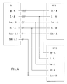
Es wird nun die Figur 2 beschrieben. Sie stellt ein Blockschaltbild des ersten bzw. zweiten Koppelfeldes KF1 bzw. KF2 dar. Es sind wieder die erste, zweite und dritte Stufe M1 , M2 und M3 und die sie bildenden Koppelmatrizen G1 bis G16 dargestellt. Jede Koppelmatrix besteht aus 256, in einer 16x16-Matrix angeordnete Koppelpunkte KP. Es sind ferner die Eingänge E1 bis E16 und die Ausgänge A1 bis A16 einer jeden Koppelmatrix angegeben.FIG. 2 will now be described. It represents a block diagram of the first and second switching matrix KF1 and KF2. The first, second and third stages M1, M2 and M3 and the coupling matrices G1 to G16 are shown again. Each coupling matrix consists of 256 coupling points KP arranged in a 16x16 matrix. The inputs E1 to E16 and the outputs A1 to A16 of each coupling matrix are also specified.
Es ist weiterhin dargestellt, wie die Eingänge E1 bis E16 der Koppelmatrizen der ersten Stufe M1 die 256 Eingänge E001 bis E256 des Koppelfeldes KF1 bzw. KF2 und die Ausgänge A1 bis A16 der Koppelmatrizen der dritten Stufe M3 die 256 Ausgänge A001 bis A256 des Koppelfeldes KF1 bzw. KF2 bilden.It is also shown how the inputs E1 to E16 of the switching matrixes of the first stage M1, the 256 inputs E001 to E256 of the switching matrix KF1 or KF2 and the outputs A1 to A16 of the switching matrixes of the third stage M3, the 256 outputs A001 to A256 of the switching matrix KF1 or form KF2.
Die Ausgänge A1 bis A16 einer jeden Koppelmatrix G1 bis G16 der ersten und der zweiten Stufe M1 , M2 sind über systematisch geführte Zwischenleitungen mit den Eingängen E1 bis E16 der Koppelmatrizen G1 bis G16 der zweiten bzw. dritten Stufe M2 bzw. M3 verbunden. Die Systematik dieser Zwischenleitungsführung ist folgende:
- Die Ordnungszahl eines Ausganges bzw. eines Einganges
- ist gleich der Ordnungszahl der Koppelmatrix, mit der
- dieser Eingang bzw. Ausgang verbunden ist.
- The ordinal number of an output or an input
- is equal to the ordinal number of the coupling matrix with which
- this input or output is connected.
Bei dem hier beschriebenen Ausführungsbeispiel bedeutet dies, daß, wie in der Figur 2 dargestellt, verbunden sind:
- a) Alle ersten Ausgänge, also A1 , der Koppelmatrizen in der ersten Stufe M1 mit der ersten Koppelmatrix, also G1, der zweiten Stufe, alle zweiten Ausgänge mit der zweiten Koppelmatrix usw..
- b) Alle ersten Eingänge, also E1, der Koppelmatrizen in der zweiten Stufe M2 mit der ersten Koppelmatrix, also G1, der ersten Stufe, alle zweiten Eingänge mit der zweiten Koppelmatrix usw..
- a) All first outputs, that is A1, of the coupling matrices in the first stage M1 with the first coupling matrix, that is to say G1, the second stage, all second outputs with the second coupling matrix, etc.
- b) All first inputs, that is E1, of the coupling matrices in the second stage M2 with the first coupling matrix, that is to say G1, of the first stage, all second inputs with the second coupling matrix, etc.
Die unter a) und b) angegebenen Verbindungen gelten sinngemäß auch für die Zwischenleitungsführung zwischen der zweiten und dritten Stufe.The connections specified under a) and b) also apply mutatis mutandis to the intermediate line routing between the second and third stages.
An Hand der Figur 3 wird der mechanische Aufbau beschrieben. Es sind zwei Schränke vorgesehen, für jedes Koppelfeld einer. Um diese Zuordnung zu verdeutlichen, wurden die Schränke mit den entsprechenden Bezugszeichen KF1 bzw. KF2 der Koppelfelder bezeichnet. Jeder Schrank enthält ein erstes, ein zweites und ein drittes Magazin M1, M2 und M3. Jedes Magazin enthält die 16 Koppelmatrizen G1 bis G16 einer Stufe. Durch die gleichlautenden Bezugszeichen M1, M2 bzw. M3 für die Magazine einerseits und die Stufen in den Figuren 1 und 2 ist die jeweilige Zuordnung angegeben.The mechanical structure is described with reference to FIG. 3. There are two cabinets, one for each switching matrix. In order to clarify this assignment, the cabinets were designated with the corresponding reference numbers KF1 and KF2 of the coupling fields. Each cabinet contains a first, a second and a third magazine M1, M2 and M3. Each magazine contains the 16 coupling matrices G1 to G16 of one level. The respective assignment is indicated by the identical reference symbols M1, M2 and M3 for the magazines on the one hand and the stages in FIGS. 1 and 2.
Jede Koppelmatrix ist als Steckbaugruppe ausgebildet. Da gemäß den Figuren 1 oder 2 jede Stufe 16 Koppelmatrizen umfaßt, enthält auch jedes Magazin 16 Steckbaugruppen. Im ersten Magazin M1 des ersten Schrankes KF1 sind diese 16 Steckbaugruppen eingezeichnet, wobei die erste mit G1 und die letzte mit G16 bezeichnet wurde. Durch die Wahl der gleichen Bezugszeichen G1 bis G16 wird wieder die Zuordnung zu den in den Figuren 1 und 2 gezeichneten Koppelmatrizen angegeben. Mit P1 und P2 wurde die erste bzw. zweite Parallelverkabelung bezeichnet.Each coupling matrix is designed as a plug-in module. Since each stage comprises 16 coupling matrices according to FIGS. 1 or 2, each magazine also contains 16 plug-in modules. These 16 plug-in modules are shown in the first magazine M1 of the first cabinet KF1, the first being designated G1 and the last G16. By selecting the same reference numerals G1 to G16, the assignment to the coupling matrices shown in FIGS. 1 and 2 is again indicated. The first and second parallel cabling were designated P1 and P2.
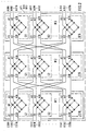
An Hand der Figur 4 wird die Steuerung der zwei Koppelfelder KF1 und KF2 durch eine gemeinsame Steuerung St gezeigt. Diese Steuerung weist je vier Ausgänge für die den durchzuschaltenden Koppelpunkt kennzeichnenden Adressen, nämlich für die Spalten-Adresse Sp.-A, für die Zeilen-Adresse Z.-A. und für die Koppelmatrix-Adresse Km.-A. sowie zwei Ausgänge für die Stufen-Adresse St.-A., auf. Diese Ausgänge sind über jeweils vier bzw. zwei Drähte mit den gleichnamigen Eingängen der Koppelfeler KF1 und KF2 verbunden. Da jede Koppelmatrix entsprechend ihren 16 Ein- und 16 Ausgängen 16 Spalten und 16 Zeilen aufweist, jede Stufe 16 Koppelmatrizen enthält und jedes Koppelfeld 3 Stufen aufweist, genügen bei Anwendung der binären Kodierung zur eindeutigen Kennzeichnung eines durchzuschaltenden Koppelpunktes diese jeweils vier Drähte für die Spalten-, Zeilen- und Koppelmatrix-Adresse und die zwei Drähte für die Stufen-Adresse. Die Kennzeichnung des jeweiligen Schrankes bzw. Koppelfeldes KF1 oder KF2 geschieht über die einzeln geführten Drähte, welche die zwei Ausgänge Schr.-A. 1 und Schr.-A.2 für die Schrank- Adressen mit den entsprechenden Eingängen Schr.-A. in den Koppelfeldern KF1 bzw. KF2 verbinden.The control of the two switching matrixes KF1 and KF2 by a common control unit St is shown on the basis of FIG. This control has four outputs for the addresses characterizing the crosspoint to be switched through, namely for the column address Sp.-A, for the row address Z.-A. and for the coupling matrix address Km.-A. as well as two outputs for the stage address St.-A., on. These outputs are connected via four or two wires to the inputs of the same name on the Koppelfeler KF1 and KF2. Since each switching matrix has 16 columns and 16 rows, each step contains 16 switching matrices and each switching matrix has 3 steps, each using four bits is sufficient for the unambiguous identification of a switching point to be switched through. , Row and switching matrix address and the two wires for the stage address. The respective cabinet or switching matrix KF1 or KF2 is identified using the individually guided wires that connect the two outputs Schr.-A. 1 and Step A.2 for the cabinet addresses with the corresponding inputs Step A. connect in the coupling fields KF1 or KF2.
Jedes der Koppelfelder KF1 und KF2 alleine ermöglicht schon eine Verbindung eines jeden Eiganges mit jedem beliebigen Ausgang. Jedoch können Blockierungen auftreten, d.h., wenn schon mehrere Verbindungen bestehen, kann eine weitere, von einem bestimmten Eingang zu einem bestimmten Ausgang zu führende Verbindung nicht mehr durchgeschaltet werden. Durch die erfindungsgemäße Parallelschaltung zweier solcher Koppelfelder werden diese Blockierungen vermieden, so daß also die erfindungsgemäße Koppelanordnung blockierungsfrei ist.Each of the coupling fields KF1 and KF2 alone enables a connection of each input to any output. However, blockages can occur, i.e. if there are already several connections, another connection leading from a specific input to a specific output can no longer be switched through. These blockages are avoided by the parallel connection of two such switching networks according to the invention, so that the coupling arrangement according to the invention is therefore free of blocking.
Die Weiterbildung nach dem Patentanspruch 2 ermöglicht eine fehlerfreie und mit wenig Handarbeit verbundene Herstellung der Zwischenleitungen. Diese Weiterbildung wird an Hand der Figuren 5 bis 9 beschrieben.The development according to
Es wird zunächst die Figur 5 betrachtet. Sie zeigt wieder die drei Magazine M1 bis M3, und zwar hier ihre mechanische Anordnung übereinander. Das erste Magazin M1 befindet sich oben, darunter ist das zweite Magazin M2 und ganz unten das dritte Magazin M3 angeordnet. Sie sind in nicht dargestellter Weise mechanisch miteinander verbunden. Das zweite Magazin ist also sowohl dem ersten als auch dem dritten benachbart.5 is first considered. It shows the three magazines M1 to M3 again, here their mechanical arrangement one above the other. The first magazine M1 is located at the top, below that is the second magazine M2 and at the bottom the third magazine M3. They are mechanically connected to one another in a manner not shown. The second magazine is therefore adjacent to both the first and the third.
Jedes Magazin weist oben und unten je 16 Führungsleisten F auf, in die die Steckbaugruppen geführt werden. Es sind nur die unteren Führungsleisten sichtbar. Von den 48 Steckbaugruppen (16 je Magazin) ist nur die sechzehnte Steckbaugruppe G16 des dritten Magazins M3 dargestellt. Jede Steckbaugruppe trägt als Steckverbinder eine erste und eine zweite Steckerleiste S1 bzw. S2. Statt der zwei Steckerleisten S1 und S2 kann auch eine einzige, große Steckerleiste vorgesehen sein.Each magazine has 16 guide strips F at the top and bottom, into which the plug-in modules are guided. Only the lower guide bars are visible. Of the 48 plug-in modules (16 per magazine), only the sixteenth plug-in module G16 of the third magazine M3 is shown. Each plug-in module carries a first and a second plug strip S1 or S2 as plug connectors. Instead of the two connector strips S1 and S2, a single, large connector strip can also be provided.
Ferner ist eine erste und eine zweite Rückwandleiterplatte L1 bzw. L2 dargestellt. Jede trägt als Gegensteckverbinder zwei Reihen von je 16 Buchsenleisten, wobei die Buchsenleisten B1 bis B16 die obere Reihe und die Buchsenleisten B17 bis B32 die untere Reihe bilden. Die Buchsenleiste B17 und einige weitere, nicht bezeichnete Buchsenleisten sind hier nicht sichtbar. Weiter sind eine dritte und eine vierte Rückwandleiterplatte L3 bzw. L4 vorgesehen. Diese tragen nur eine Reihe von je 16 Buchsenleisten B33 bis B48 bzw. B49 bis B64.Furthermore, a first and a second backplane circuit board L1 and L2 are shown. Each carries two rows of 16 socket strips as mating connectors, with socket strips B1 to B16 forming the upper row and socket strips B17 to B32 forming the lower row. The socket strip B17 and some other socket strips, not shown, are not visible here. A third and a fourth backplane L3 and L4 are also provided. These only carry a row of 16 socket strips B33 to B48 or B49 to B64.
Durch gestrichelte Linien ist angedeutet, in welche der Führungsleisten die dargestellte Steckbaugruppe G16 bei ihrem Einstecken geführt wird, welche Lage die Rückwandleiterplatten an der Rückseite der Magazine nach dem Zusammenbau einnehmen sowie daß die Steckerleisten S1 und S2 der dargestellten Steckbaugruppe G16 in die Buchsenleiste B32 der zweiten Rückwandleiterplatte L2 und die Buchsenleiste B64 der vierten Rückwandleiterplatte L4 eingreifen. In der gleichen Weise greifen die Steckerleisten der nicht dargestellten Steckbaugruppen in die ihnen zugeordneten Buchsenleisten ein. So ergibt sich eine Zuordnung gemäß der folgenden Tabelle:

Die Rückwandleiterplatte L1 umfaßt also den Bereich der Steckerleisten S2 des ersten Magazins M1 und den Bereich der Steckerleisten S1 des zweiten Magazins M2. Der Bereich der Steckerleisten S2 des ersten Magazins M1 ist dem Bereich der Steckerleisten S1 des zweiten Magazins M2 benachbart. Das gleiche gilt sinngemäß für die Rückwandleiterplatte L2.The backplane circuit board L1 thus comprises the area of the connector strips S2 of the first magazine M1 and the area of the connector strips S1 of the second magazine M2. The area of the connector strips S2 of the first magazine M1 is adjacent to the area of the connector strips S1 of the second magazine M2. The same applies analogously to the backplane L2.
In der Figur 6 ist eine der Steckbaugruppen G1 bis G16 dargestellt. Sie besteht aus einer Leiterplatte LP, welche die 256, in einer 16x16-Matrix angeordneten Koppelpunkte KP, eine erste Steckerleiste S1 und eine zweite Steckerleiste S2 trägt. Die Leiterplatte LP weist Leiterbahnen LB auf, die die Koppelpunkte KP untereinander sowie mit den 16 Eingängen E1 bis E16 und den 16 Ausgängen A1 bis A16 auf den Steckerleisten S1 bzw. S2 verbinden. Die Eingänge E1 bis E16 sind alle auf der ersten Steckerleiste S1 , die Ausgänge A1 bis A16 sind alle auf der zweiten Steckerleiste S2 herausgeführt. Wie aus der Figur 5 hervorgeht, ist bei den Steckbaugruppen des zweiten Magazins M2 die erste Steckerleiste S1 dem ersten Magazin M1 am nächsten gelegen. Deshalb sind auf ihr die Eingänge E1 bis E16 herausgeführt, weil diese gemäß der Figur 2 mit den Ausgängen der Steckbaugruppen des ersten Magazins M1 verbunden werden müssen. Das Gleiche gilt sinngemäß für die zweiten Steckerleisten S2 und für die Steckbaugruppen der anderen Magazine.FIG. 6 shows one of the plug-in modules G1 to G16. It consists of a printed circuit board LP, which carries the 256 coupling points KP arranged in a 16x16 matrix, a first connector strip S1 and a second connector strip S2. The printed circuit board LP has conductor tracks LB which connect the coupling points KP to one another and to the 16 inputs E1 to E16 and the 16 outputs A1 to A16 on the connector strips S1 and S2. The inputs E1 to E16 are all on the first connector S1, the outputs A1 to A16 are all led out on the second connector S2. As can be seen from FIG. 5, in the plug-in modules of the second magazine M2, the first connector strip S1 is closest to the first magazine M1. Therefore, the inputs E1 to E16 are brought out on it, because according to FIG. 2 they have to be connected to the outputs of the plug-in modules of the first magazine M1. The same applies analogously for the second connector strips S2 and for the plug-in modules of the other magazines.
Die Leiterbahnen LB wurden hier einpolig dargestellt. Da Koppelfelder jedoch üblicherweise zwei- oder gar vieradrig ausgeführt werden, muß man sich anstelle einer Linie zwei bzw. vier Leiterbahnen und auf den Steckerleisten entsprechend viele Steckerstifte vorstellen.The conductor tracks LB were shown here as single-pole. However, since switching matrixes are usually made with two or even four wires, you have to imagine two or four conductor tracks instead of a line and a corresponding number of connector pins on the connector strips.
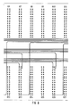
In den Figuren 7, 8 und 9 ist eine der Rückwandleiterplatten L1 bzw. L2 dargestellt. Diese Figuren lege man nebeneinander, die Figur 7 links und die Figur 9 rechts. Die jeweils obere und untere Linie sowie die linke bzw. rechte Linie auf der Figur 7 bzw. 9 geben die Umrisse dieser Rückwandleiterplatte an. Mit B1 bis B16 (obere Reihe) und B17 bis B32 sind die Plätze für die Buchsenleisten B1 bis B32 bezeichnet. Diese Buchsenleisten selbst sind nicht dargestellt, sondern es sind durch Punkte nur die Lötaugen für ihre Lötstifte angedeutet. Betrachtet man die erste Rückwandleiteplatte L1, so liegen, wie aus den Figuren 5 und 6 hervorgeht, auf den Buchsenleisten B1 bis B16 die Ausgänge A1 bis A16 der Steckbaugruppen G1 bis G16 aus dem ersten Magazin M1. Auf den Buchsenleisten B17 bis B32 liegen die Eingänge E1 bis E16 der Steckbaugruppen des zweiten Magazins M2, und zwar jeweils oben mit E1 bzw. A1 beginnend.FIGS. 7, 8 and 9 show one of the backplane circuit boards L1 and L2. Place these figures next to each other, Figure 7 on the left and Figure 9 on the right. The respective upper and lower lines as well as the left and right lines on FIGS. 7 and 9 indicate the outlines of this backplane. B1 to B16 (top row) and B17 to B32 denote the locations for the socket strips B1 to B32. These socket strips themselves are not shown, but only the pads for their soldering pins are indicated by dots. If one looks at the first backplane L1, as can be seen from FIGS. 5 and 6, the outputs A1 to A16 of the plug-in modules G1 to G16 from the first magazine M1 lie on the socket strips B1 to B16. The inputs E1 to E16 of the plug-in modules of the second magazine M2 are located on the socket strips B17 to B32, starting at the top with E1 and A1.
Die Zwischenleitungen, die gemäß der Figur 2 zu schaffen sind, werden durch Leiterbahnen LB' gebildet. Dabei wurde hier wieder eine einpolige Darstellung gewählt; und man muß sich anstelle einer Linie zwei Leiterbahnen vorstellen, da, wie an der Darstellung von je zwei Lötaugen für jeden Ein- bzw. Ausgang zu erkennen ist, hier eine Rückwandleiterplatte für ein zweiadriges Koppelfeld gezeichnet ist. Von den vielen Zwischenleitungen sind hier nur einige gezeichnet. Außerdem ist nicht gezeichnet, daß die Leiterbahnen auf verschiedene Ebenen einer Multilayerplatte verteilt sind, um ihre große Zahl unterbringen und ihre Kreuzungen ausführen zu können.The intermediate lines which are to be created according to FIG. 2 are formed by conductor tracks LB '. A single-pole display was chosen here again; and one has to imagine two conductor tracks instead of a line, since, as can be seen from the illustration of two solder eyes for each input and output, here a backplane for a two-wire switching matrix is drawn. Only a few of the many intermediate lines are shown here. In addition, it is not shown that the conductor tracks are distributed over different levels of a multilayer board in order to accommodate their large number and to be able to cross them.
Die zweite Rückwandleiterplatte ist wie die erste ausgeführt, da laut Figur 2 die Systematik der Zwischenleitungsführung zwischen der ersten und der zweiten Stufe derjenigen zwischen der zweiten und dritten Stufe gleicht.The second backplane is designed like the first, since, according to FIG. 2, the system of the intermediate line routing between the first and the second stage is the same as that between the second and third stages.
Auf den Buchsenleisten B33 bis B48 der dritten Rückwandleiterplatte L3 liegen die 256 Eingänge E001 bis E256 und auf den Buchsenleisten B49 bis B64 der vierten Rückwandleiterplatte L4 liegen die Ausgänge A001 bis A256 des jeweiligen Koppelfeldes KF1 bzw. KF2. An den Lötstiften dieser Buchsenleisten sind die Parallelverdrahtungen P1 und P2 sowie die Verbindungen zu den Signalquellen Q und den Signalsenken S angeschlossen.The 256 inputs E001 to E256 are on the socket strips B33 to B48 of the third backplane L3 and the outputs A001 to A256 of the respective switching matrix KF1 or KF2 are on the socket strips B49 to B64 of the fourth backplane L4. The parallel wiring P1 and P2 as well as the connections to the signal sources Q and the signal sinks S are connected to the solder pins of these socket strips.
Nicht dargestellt sind Schaltmittel und Steuerleitungen zum Durchschalten und Ausschalten der Koppelpunkte. Dies gilt auch für die Steckbaugruppen.Switching means and control lines for switching the switching points on and off are not shown. This also applies to the plug-in modules.
Durch die Weiterbildung gemäß dem Patentanspruch 3 wird erreicht, daß die erfindungsgemäße Koppelanordnung zur Übertragung von Digitalsignalen mit einer Bitrate bis zu 150 MBit/s geeignet ist.The development according to claim 3 ensures that the coupling arrangement according to the invention is suitable for the transmission of digital signals with a bit rate of up to 150 Mbit / s.
Dazu gehört, daß bei dieser hohen Bitrate noch eine ausreichend hohe Nebensprechdämpfung zwischen den Leiterbahnen einer Rückwandleiterplatte L1 bzw. L2 besteht. Wie diese hohe Nebensprechdämpfung erreicht wird, sei an Hand der Figur 10 erläutert. Sie zeigt einen Schnitt durch eine solche Rückwandleiterplatte, um die Lage der Leiterbahnen in ihr darzustellen. Sie weist 19 Schichten auf, zwischen denen die schraffiert gezeichneten Leiterbahnen liegen. Es wird ein zweiadrig aufgebautes Koppelfeld angenommen, d.h., jede Verbindung ist als ein Paar von Leiterbahnen ausgeführt. Das erste Paar ist mit LB1 bezeichnet und liegt in der ersten Ebene zwischen der ersten und zweiten Schicht. Um eine ausreichend hohe Nebensprechdämpfung zu erreichen, ist das zweite Paar LB2 in der nächsten, also zweiten Ebene nicht unmittelbar neben dem ersten Paar LB1 angeordnet, sondern entsprechend der Nebensprechdämpfungsforderung seitlich versetzt. Diese Versetzung erstreckt sich über acht Ebenen. Die neunte und zehnte Ebene trägt die Leiterbahnen StL für die in den Figuren 7 bis 9 nicht dargestellten Steuerleitungen. Die gegebenen Nebensprechdämpfungsforderungen erlauben es erst, in der elften Ebene wieder ein Paar LB3 ohne Versetzung gegenüber dem ersten Paar LB1 anzuordnen.This includes that at this high bit rate there is still a sufficiently high crosstalk attenuation between the conductor tracks of a backplane L1 or L2. How this high crosstalk attenuation is achieved will be explained with reference to FIG. 10. It shows a section through such a backplane to show the position of the conductor tracks in it. It has 19 layers, between which the hatched conductor tracks lie. A two-wire switching matrix is assumed, i.e. each connection is designed as a pair of conductor tracks. The first pair is labeled LB1 and lies on the first level between the first and second layers. In order to achieve a sufficiently high crosstalk attenuation, the second pair LB2 is not arranged directly next to the first pair LB1 in the next, that is to say the second level, but is laterally offset in accordance with the crosstalk attenuation requirement. This transfer extends over eight levels. The ninth and tenth levels carry the conductor tracks StL for the control lines not shown in FIGS. 7 to 9. The given crosstalk attenuation requirements only allow a pair LB3 to be arranged again in the eleventh level without displacement relative to the first pair LB1.
Dazu gehört auch, daß die Leiterbahnen der Rückwandleiterplatten keine Stoßstellen aufweisen. Um solche Stoßstellen zu vermeiden, sind, wie in den Figuren 7 bis 9 zu erkennen ist, spitzwinklige Abknickungen der Leiterbahnen ganz vermieden und rechtwinklige in zwei stumpfwinklige aufgelöst. Statt der Auflösung in stumpfwinklige Abknickungen ist eine abgerundete Ausführung möglich. Dies gilt auch für die Leiterbahnen der Steckbaugruppen. Falls sich spitzwinklige Abknickungen nicht vermeiden lassen, werden sie ebenfalls in mehrere stumpfwinklige aufgelöst oder abgerundet ausgeführt.This also means that the conductor tracks of the backplane have no joints. In order to avoid such joints, as can be seen in FIGS. 7 to 9, acute-angled kinks in the conductor tracks are completely avoided and right-angled ones are dissolved in two obtuse-angled ones. Instead of the resolution in obtuse-angled bends, a rounded version is possible. This also applies to the conductor tracks of the plug-in modules. If acute-angled kinks cannot be avoided, they are also broken up into several obtuse-angled ones or rounded off.
Dazu gehört ferner, daß die Signalquellen Q reflexionsfrei mit den Eingängen E001 bis E256 verbunden sind. Wie dies erreicht wird, sei an Hand der Figur 11 erläutert. Es sind die zwei Schränke bzw. Koppelfelder KF1 und KF2 und die in ihnen befindlichen Rückwandleiterplatten L3 angedeutet. Die Punkte stellen die Lötstifte der Buchsenleisten B33 bis B48 dar. Ein nicht bezeichnetes Kabel führt von den Signalquellen Q zu den Buchsenleisten B33 bis B48 im ersten Schrank KF1, und die Drähte aus diesem Kabel sind an die Lötstifte dieser Buchsenleisten angelötet. Von diesen Drähten sind nur einige dargestellt. An diese Lötstifte sind ferner die Drähte der Parallelverkabelung P1 angelötet. Diese Drähte enden andererseits auf den Löststiften der Buchsenleisten B33 bis B48 des zweiten Schrankes KF2. An diesen Lötstiften sind außerdem Widerstände R angeschlossen. Ihr Widerstandswert ist gleich dem Wellenwiderstand der Parallelverkabelung P1 und des von den Signalquellen Q kommenden Kabels gewählt. Diese Widerstände bewirken den erforderlichen reflexionsfreien Abschluß, da die Koppelmatrizen selbst, wegen ihres hohen Eingangswiderstandes einen solchen Abschluß nicht bieten können. Statt des Lötens ist auch jede andere Verbindungstechnik anwendbar. Die Widerstände R und das von den Signalquellen kommende Kabel können auch vertauscht sein, d.h. das Kabel endet im zweiten Schrank KF2 und die Widerstände R befinden sich im ersten Schrank KF1.This also includes that the signal sources Q are connected to the inputs E001 to E256 without reflection. How this is achieved will be explained with reference to FIG. 11. The two cabinets or coupling fields KF1 and KF2 and the backplane L3 located in them are indicated. The dots represent the soldering pins of the socket strips B33 to B48. A cable that is not labeled leads from the signal sources Q to the socket strips B33 to B48 in the first cabinet KF1, and the wires from this cable are soldered to the soldering pins of these socket strips. Only a few of these wires are shown. The wires of the parallel wiring P1 are also soldered to these soldering pins. These wires end on the other hand on the release pins of the socket strips B33 to B48 of the second cabinet KF2. Resistors R are also connected to these solder pins. Their resistance value is chosen equal to the characteristic impedance of the parallel cabling P1 and the cable coming from the signal sources Q. These resistors bring about the required reflection-free termination, since the coupling matrices themselves cannot offer such a termination because of their high input resistance. Instead of soldering, any other connection technology can also be used. The resistors R and the cable coming from the signal sources can also be interchanged, ie the cable ends in the second cabinet KF2 and the resistors R are in the first cabinet KF1.
Die entsprechende Ausbildung der ausgangsseitigen "Parallelverkabelung" wird an Hand der Figur 12 beschrieben. Es sind die zwei Schränke KF1 und KF2 mit ihren je 256 Ausgängen A001 bis A256 sowie 256 elektronische Umschalter U001 bis U256 angedeutet. Jeder der Ausgänge A001 bis A256 ist mit dem zugehörigen ersten bzw. zweiten Eingang des zugehörigen elektronischen Umschalters U001 bis U256 verbunden. Die Ausgänge der elektronischen Umschalter sind mit den Signalsenken S verbunden. Die elektronischen Umschalter weisen ferner Steuereingänge auf, die mit einer Umschaltsteuerung U.-St. verbunden sind. So kann diese Umschaltsteuerung die elektronischen Umschalter in ihre erste oder zweite Schaltstellung steuern. Hier ist die erste Schaltstellung gezeichnet, in der der jeweilige Ausgang der ersten Koppelfeldes KF1 zur betreffenden Signalsenke S durchgeschaltet ist.The corresponding design of the "parallel cabling" on the output side is described with reference to FIG. The two cabinets KF1 and KF2 with their 256 outputs A001 to A256 and 256 electronic changeover switches U001 to U256 are indicated. Each of the outputs A001 to A256 is connected to the associated first or second input of the associated electronic switch U001 to U256. The outputs of the electronic changeover switches are connected to the signal sinks S. The electronic changeover switches also have control inputs which are controlled by a changeover control U.-St. are connected. This changeover control can thus control the electronic changeover switch into its first or second switching position. Here the first switching position is drawn, in which the respective output of the first switching matrix KF1 is switched through to the relevant signal sink S.
Da die Koppelmatrizen G1 bis G16 ausgangsseitig schon Abschlußwiderstände aufweisen, ist eine ausgangsseitige einfache Parallelschaltung wie bei den Eingängen nicht möglich. Vielmehr darf nur einer der betreffenden Ausgänge der Koppelfelder KF1 bzw. KF2 zu der betreffenden Signalsenke S durchgeschaltet werden. Dies bewirken die elektronischen Umschalter U001 bis U256 in Abhängigkeit davon, ob die jeweilige Verbindung über das erste Koppelfeld KF1 oder über das zweite Koppelfeld KF2 durchgeschaltet wurde. Die dazu nötige Einstellinformation gewinnt die Umschaltsteuerung U.-St. aus der Spalten-Adresse Sp.-A., der Zeilen-Adresse Z.-A., der Koppelmatrix-Adresse Km.-A., der Stufen-Adressen St.-A. sowie den Schrank-Adressen Schr.-A.1 und Schr.-A.2. Sie ist deshalb mit den entsprechenden, in der Beschreibung der Figur 4 schon erwähnten Ausgängen der Steuerung St verbunden.Since the coupling matrices G1 to G16 already have terminating resistors on the output side, a simple parallel connection on the output side is not possible, as is the case with the inputs. Rather, only one of the relevant outputs of the switching networks KF1 or KF2 may be switched through to the relevant signal sink S. This is caused by the electronic changeover switches U001 to U256, depending on whether the respective connection was switched through via the first switching matrix KF1 or via the second switching matrix KF2. The switching control U.-St. from the column address Sp.-A., the row address Z.-A., the coupling matrix address Km.-A., the step addresses St.-A. and the cabinet addresses Schr.-A.1 and Schr.-A.2. It is therefore connected to the corresponding outputs of the control unit St already mentioned in the description of FIG.
Eine vorteilhafte Ausführung der elektronischen Umschalter wird an Hand der Figur 13 beschrieben. Um eine Typenvielfalt von Steckbaugruppen zu vermeiden, werden als elektronische Umschalter die gleichen Koppelmatrizen verwendet wie sie in den Koppelfeldern KF1 und KF2 eingesetzt und an Hand der Figur 6 beschrieben sind. Eine solche Koppelmatrix ist auch in der Figur 13 dargestellt und dort mit GU1 bezeichnet. Es sind durch Kreise die 256 Koppelpunkte angedeutet. Die Eingänge E1 bis E8 sind mit den Ausgängen A001 bis A008 des ersten Koppelfeldes KF1 verbunden. Die Eingänge E9 bis E16 sind mit den Ausgängen A001 bis A008 des zweiten Koppelfeldes KF2 verbunden. An die Ausgänge A1 bis A8 dieser Koppelmatrix sind die zugehörigen 8 Signalsenken S angeschlossen.An advantageous embodiment of the electronic changeover switch is described with reference to FIG. 13. In order to avoid a variety of types of plug-in modules, the same coupling matrices are used as electronic changeover switches as are used in the coupling fields KF1 and KF2 and are described with reference to FIG. 6. Such a coupling matrix is also shown in FIG. 13 and labeled GU1 there. The 256 crosspoints are indicated by circles. The inputs E1 to E8 are connected to the outputs A001 to A008 of the first switching matrix KF1. The inputs E9 to E16 are connected to the outputs A001 to A008 of the second switching matrix KF2. The associated 8 signal sinks S are connected to the outputs A1 to A8 of this coupling matrix.
Die Funktion ist folgende: Soll z.B. eine Verbindung zu der am Ausgang A1 der Koppelmatrix GU1 angeschlossenen Signalsenke durchgeschaltet werden, so wird in dieser Koppelmatrix entweder der den Eingang E1 oder der den Eingang E9 mit dem Ausgang A1 verbindende Koppelpunkt durchgeschaltet, je nach dem, ob die Verbindung über das erste oder zweite Koppelfeld KF1 bzw. KF2 geführt wird. In der sinngemäß gleichen Weise wird bei einem Verbindungsaufbau zu den anderen Ausgängen verfahren. Die dazu jeweils benötigten Koppelpunkte sind in der Figur 13 durch zwei Kreise hervorgehoben.The function is as follows: a connection to the signal sink connected to the output A1 of the coupling matrix GU1 is switched through, then in this coupling matrix either the coupling point connecting the input E1 or the input E9 with the output A1 is switched through, depending on whether the connection is via the first or the second Coupling field KF1 or KF2 is performed. The same procedure is followed when establishing a connection to the other outputs. The coupling points required for this are highlighted in FIG. 13 by two circles.
In der gleichen Weise werden die weiteren Ausgänge A009 bis A256 der Koppelfelder KF1 und KF2 zusammengeschaltet. So ergeben sich 32 solcher Koppelmatrizen. Ihre Unterbringung wird an Hand der Figur 14 beschrieben. Die zwei Schränke KF1 und KF2 enthalten zusätzlich zu den Magazinen M1 bis M3 noch die vierten Magazine M4, welche die 32 Koppelmatrizen GU1 bis GU32 aufnehmen. Die Koppelmatrizen GU1 bis GU16 befinden sich im ersten Schrank KF1, die Koppelmatrizen GU17 bis GU32 befinden sich im zweiten Schrank KF2.The other outputs A009 to A256 of switching matrixes KF1 and KF2 are interconnected in the same way. This results in 32 such coupling matrices. Your accommodation is described with reference to Figure 14. In addition to the magazines M1 to M3, the two cabinets KF1 and KF2 also contain the fourth magazines M4, which hold the 32 coupling matrices GU1 to GU32. The coupling matrices GU1 to GU16 are in the first cabinet KF1, the coupling matrices GU17 to GU32 are in the second cabinet KF2.
Eine vorteilhafte Verdrahtung zwischen den Ausgängen A001 bis A256 der Koppelfelder KF1 bzw. KF2 und den Eingängen E1 bis E8 der Koppelmatrizen GU1 bis GU32 wird an Hand der Figur 15 beschrieben. Es sind durch jeweils 32 Punkte die Lötstifte der Buchsenleisten B49 des ersten und des zweiten Koppelfeldes KF1 bzw. KF2 dargestellt, auf denen die Ausgänge A001 bis A016 liegen. Ebenfalls durch je 32 Punkte sind die Lötstifte derjenigen Buchsenleisten dargestellt, auf denen die Eingänge E1 bis E16 der Koppelmatrizen GU1 und GU2 liegen. Es sind zwei Bandkabel BK1 und BK2 vorgesehen, wobei jedes 16 nebeneinander geführte Adernpaare aufweist. Über das erste Bandkabel BK1 sind die Ausgänge A001 bis A016 des ersten Koppelfeldes KF1 mit den Eingängen E1 bis E8 der Koppelmatrizen GU1 und GU2 verbunden. Über das zweite Bandkabel BK2 sind die Ausgänge A001 bis A016 des zweiten Koppelfeldes KF2 mit den Eingängen E9 bis E16 der Koppelmatrizen GU1 und GU2 verbunden. Die Bandkabel sind in der Mitte soweit längs geschlitzt, damit sich genügend lange Enden zum Anschluß auf den Buchsenleisten der Koppelmatrizen GU1 bzw. GU2 ergeben.An advantageous wiring between the outputs A001 to A256 of the switching matrixes KF1 and KF2 and the inputs E1 to E8 of the switching matrixes GU1 to GU32 is described with reference to FIG. The solder pins of the socket strips B49 of the first and the second switching matrix KF1 and KF2, on which the outputs A001 to A016 are located, are represented by 32 points each. The soldering pins of the socket strips on which the inputs E1 to E16 of the coupling matrices GU1 and GU2 are located are also represented by 32 points each. Two ribbon cables BK1 and BK2 are provided, each of which has 16 pairs of wires which are guided next to one another. The outputs A001 to A016 of the first switching matrix KF1 are connected to the inputs E1 to E8 of the switching matrixes GU1 and GU2 via the first ribbon cable BK1. The outputs A001 to A016 of the second switching matrix KF2 are connected to the inputs E9 to E16 of the switching matrixes GU1 and GU2 via the second ribbon cable BK2. The ribbon cables are slotted longitudinally in the middle so that there are enough long ends for connection to the socket strips of the coupling matrices GU1 and GU2.
In der gleichen Weise sind über jeweils zwei Bandkabel die weiteren Ausgänge der Koppelfelder KF1 und KF2 mit den zugehörigen Koppelmatrizen GU3 bis GU32 verbunden.In the same way, the further outputs of the switching matrixes KF1 and KF2 are connected to the associated switching matrixes GU3 to GU32 via two ribbon cables.
Die Anwendung von Bandkabel wird durch die an Hand der Figur 13 erläuterten Zuordnung von jeweils acht Ausgängen der Koppelfelder KF1 und KF2 zu jeweils den Eingängen A1 bis A8 oder A9 bis A16 einer der Koppelmatrizen GU1 bis GU32 ermöglicht. Durch die Verwendung der Bandkabel wird erreicht, daß diese Verbindungen elektrische Eigenschaften mit geringen Exemplarstreuungen aufweisen und damit für die Übertragung von Digitalsignalen mit hoher Bitrate geeignet sind.The use of ribbon cables is made possible by the assignment of eight outputs of the coupling fields KF1 and KF2 to the inputs A1 to A8 or A9 to A16 of one of the coupling matrices GU1 to GU32 explained with reference to FIG. 13. The use of the ribbon cable ensures that these connections have electrical properties with little specimen scatter and are therefore suitable for the transmission of digital signals at a high bit rate.
Claims (3)
Priority Applications (6)
| Application Number | Priority Date | Filing Date | Title |
|---|---|---|---|
| AT86104544T ATE65006T1 (en) | 1986-04-03 | 1986-04-03 | THREE-STAGE COUPLING ARRANGEMENT. |
| DE8686104544T DE3680100D1 (en) | 1986-04-03 | 1986-04-03 | THREE-STAGE COUPLING. |
| EP86104544A EP0240580B2 (en) | 1986-04-03 | 1986-04-03 | Three-stage coupling arrangement |
| CA000533544A CA1285055C (en) | 1986-04-03 | 1987-04-01 | Three-stage coupling arrangement |
| DK168887A DK168887A (en) | 1986-04-03 | 1987-04-02 | STEP STEP CONNECTING NETWORK |
| US07/038,126 US4862161A (en) | 1985-01-24 | 1987-04-02 | Three-stage coupling arrangement |
Applications Claiming Priority (1)
| Application Number | Priority Date | Filing Date | Title |
|---|---|---|---|
| EP86104544A EP0240580B2 (en) | 1986-04-03 | 1986-04-03 | Three-stage coupling arrangement |
Publications (3)
| Publication Number | Publication Date |
|---|---|
| EP0240580A1 EP0240580A1 (en) | 1987-10-14 |
| EP0240580B1 true EP0240580B1 (en) | 1991-07-03 |
| EP0240580B2 EP0240580B2 (en) | 1994-11-17 |
Family
ID=8195036
Family Applications (1)
| Application Number | Title | Priority Date | Filing Date |
|---|---|---|---|
| EP86104544A Expired - Lifetime EP0240580B2 (en) | 1985-01-24 | 1986-04-03 | Three-stage coupling arrangement |
Country Status (5)
| Country | Link |
|---|---|
| EP (1) | EP0240580B2 (en) |
| AT (1) | ATE65006T1 (en) |
| CA (1) | CA1285055C (en) |
| DE (1) | DE3680100D1 (en) |
| DK (1) | DK168887A (en) |
Families Citing this family (3)
| Publication number | Priority date | Publication date | Assignee | Title |
|---|---|---|---|---|
| DE3802579A1 (en) * | 1988-01-29 | 1989-08-10 | Ant Nachrichtentech | THREE-STAGE NON-BLOCKING DOMESTIC |
| US5008881A (en) * | 1990-05-18 | 1991-04-16 | At&T Bell Laboratories | Chordal ring network |
| DE102004031149A1 (en) * | 2004-06-28 | 2005-09-01 | Siemens Ag | Magnetic resonance coil output signal distribution network has crossbar part networks connected through matching networks at inputs and outputs |
Family Cites Families (3)
| Publication number | Priority date | Publication date | Assignee | Title |
|---|---|---|---|---|
| DE2500939B2 (en) * | 1975-01-11 | 1977-02-10 | Licentia Patent-Verwaltungs-Gmbh, 6000 Frankfurt | CROSS CONTROL PANEL |
| DE2542579A1 (en) * | 1975-09-24 | 1977-04-07 | Siemens Ag | Coupling field for communication systems - consists of coupling multiples with same order inputs and outputs connected to four wire lines |
| DE3502295A1 (en) * | 1985-01-24 | 1986-07-24 | ANT Nachrichtentechnik GmbH, 7150 Backnang | CONSTRUCTION SYSTEM FOR ELECTRICAL COMMUNICATION DEVICES |
-
1986
- 1986-04-03 EP EP86104544A patent/EP0240580B2/en not_active Expired - Lifetime
- 1986-04-03 DE DE8686104544T patent/DE3680100D1/en not_active Expired - Lifetime
- 1986-04-03 AT AT86104544T patent/ATE65006T1/en not_active IP Right Cessation
-
1987
- 1987-04-01 CA CA000533544A patent/CA1285055C/en not_active Expired - Fee Related
- 1987-04-02 DK DK168887A patent/DK168887A/en not_active IP Right Cessation
Also Published As
| Publication number | Publication date |
|---|---|
| DK168887D0 (en) | 1987-04-02 |
| ATE65006T1 (en) | 1991-07-15 |
| EP0240580A1 (en) | 1987-10-14 |
| CA1285055C (en) | 1991-06-18 |
| DE3680100D1 (en) | 1991-08-08 |
| DK168887A (en) | 1987-10-04 |
| EP0240580B2 (en) | 1994-11-17 |
Similar Documents
| Publication | Publication Date | Title |
|---|---|---|
| EP0191902B1 (en) | Structure system for electrical-information technology apparatuses | |
| EP0712267B1 (en) | Modular control equipment with field bus integrated connection | |
| US4862161A (en) | Three-stage coupling arrangement | |
| DE2539865C3 (en) | Main distributor for a telephone exchange | |
| EP1527503B1 (en) | Distributor connection module for telecommunication and data technology | |
| DE19623470C2 (en) | Automatic line distribution device | |
| DE2432441A1 (en) | CROSS CONNECTING SWITCH | |
| DE2349444A1 (en) | CONNECTOR SWITCH | |
| EP0364658A2 (en) | Distribution device, especially for the main distributor of telephone exchanges | |
| DE2927219A1 (en) | SWITCHING MATRIX FOR CIRCUITING BROADBAND RF SIGNALS | |
| WO2006122698A1 (en) | Active distribution device in a subscriber connection area | |
| EP0240580B1 (en) | Three-stage coupling arrangement | |
| EP1503307B1 (en) | Emulation device for integrated circuit design | |
| EP0270185B1 (en) | Broadband multiple field with interconnections on a conductor plate with multiple layers in microstrip technique | |
| DE69821231T2 (en) | CONNECTING DEVICE WITH SIGNAL BUS | |
| EP0037882B1 (en) | Multi-stage coupling field | |
| DE2538656A1 (en) | Telephone exchange line interconnection system - uses three-dimensional cubical lattic framework with couplers at nodal points | |
| DE2846626A1 (en) | REMOTE LINE CONTROL SYSTEM | |
| DE4446656C2 (en) | Control system for telecommunication systems | |
| DE2545976B1 (en) | Telephone exchange binary code addressed units - identical units connected by decoding units to common line to simplify construction and maintenance | |
| DE4129332A1 (en) | Bus system for plug in processor modules for NC application - has local bus structure on each plug in module with interconnection provided by main bus | |
| DE2247523A1 (en) | ELECTRICAL OR ELECTRONIC COUPLING ARRANGEMENTS FOR REMOTE COMMUNICATION, IN PARTICULAR TELEPHONE SWITCHING SYSTEMS | |
| EP0636303B1 (en) | Assembly for a distributor rack in a telecommunications network | |
| EP1104611B1 (en) | Switching matrix for a communication network | |
| EP0378114B1 (en) | Arrangement for forming a PCM line structure in a digital communication system |
Legal Events
| Date | Code | Title | Description |
|---|---|---|---|
| PUAI | Public reference made under article 153(3) epc to a published international application that has entered the european phase |
Free format text: ORIGINAL CODE: 0009012 |
|
| AK | Designated contracting states |
Kind code of ref document: A1 Designated state(s): AT BE DE FR GB IT NL SE |
|
| 17P | Request for examination filed |
Effective date: 19871030 |
|
| 17Q | First examination report despatched |
Effective date: 19891031 |
|
| GRAA | (expected) grant |
Free format text: ORIGINAL CODE: 0009210 |
|
| AK | Designated contracting states |
Kind code of ref document: B1 Designated state(s): AT BE DE FR GB IT NL SE |
|
| ITF | It: translation for a ep patent filed |
Owner name: BARZANO' E ZANARDO MILANO S.P.A. |
|
| REF | Corresponds to: |
Ref document number: 65006 Country of ref document: AT Date of ref document: 19910715 Kind code of ref document: T |
|
| GBT | Gb: translation of ep patent filed (gb section 77(6)(a)/1977) | ||
| REF | Corresponds to: |
Ref document number: 3680100 Country of ref document: DE Date of ref document: 19910808 |
|
| ET | Fr: translation filed | ||
| PLBI | Opposition filed |
Free format text: ORIGINAL CODE: 0009260 |
|
| 26 | Opposition filed |
Opponent name: PHILIPS PATENTVERWALTUNG GMBH Effective date: 19920331 |
|
| NLR1 | Nl: opposition has been filed with the epo |
Opponent name: PHILIPS PATENTVERWALTUNG GMBH. |
|
| PG25 | Lapsed in a contracting state [announced via postgrant information from national office to epo] |
Ref country code: SE Free format text: LAPSE BECAUSE OF NON-PAYMENT OF DUE FEES Effective date: 19940404 |
|
| PGFP | Annual fee paid to national office [announced via postgrant information from national office to epo] |
Ref country code: SE Payment date: 19940425 Year of fee payment: 9 |
|
| PGFP | Annual fee paid to national office [announced via postgrant information from national office to epo] |
Ref country code: NL Payment date: 19940430 Year of fee payment: 9 |
|
| PUAH | Patent maintained in amended form |
Free format text: ORIGINAL CODE: 0009272 |
|
| STAA | Information on the status of an ep patent application or granted ep patent |
Free format text: STATUS: PATENT MAINTAINED AS AMENDED |
|
| 27A | Patent maintained in amended form |
Effective date: 19941117 |
|
| AK | Designated contracting states |
Kind code of ref document: B2 Designated state(s): AT BE DE FR GB IT NL SE |
|
| PG25 | Lapsed in a contracting state [announced via postgrant information from national office to epo] |
Ref country code: NL Effective date: 19941117 |
|
| NLR2 | Nl: decision of opposition | ||
| GBTA | Gb: translation of amended ep patent filed (gb section 77(6)(b)/1977) |
Effective date: 19941221 |
|
| EUG | Se: european patent has lapsed |
Ref document number: 86104544.1 Effective date: 19950222 |
|
| ET3 | Fr: translation filed ** decision concerning opposition | ||
| PGFP | Annual fee paid to national office [announced via postgrant information from national office to epo] |
Ref country code: GB Payment date: 19950314 Year of fee payment: 10 |
|
| PGFP | Annual fee paid to national office [announced via postgrant information from national office to epo] |
Ref country code: FR Payment date: 19950413 Year of fee payment: 10 |
|
| NLV1 | Nl: lapsed or annulled due to failure to fulfill the requirements of art. 29p and 29m of the patents act | ||
| PGFP | Annual fee paid to national office [announced via postgrant information from national office to epo] |
Ref country code: AT Payment date: 19950426 Year of fee payment: 10 |
|
| PGFP | Annual fee paid to national office [announced via postgrant information from national office to epo] |
Ref country code: BE Payment date: 19950503 Year of fee payment: 10 |
|
| PGFP | Annual fee paid to national office [announced via postgrant information from national office to epo] |
Ref country code: DE Payment date: 19951208 Year of fee payment: 10 |
|
| PG25 | Lapsed in a contracting state [announced via postgrant information from national office to epo] |
Ref country code: GB Effective date: 19960403 Ref country code: AT Effective date: 19960403 |
|
| PG25 | Lapsed in a contracting state [announced via postgrant information from national office to epo] |
Ref country code: BE Effective date: 19960430 |
|
| BERE | Be: lapsed |
Owner name: ANT NACHRICHTENTECHNIK G.M.B.H. Effective date: 19960430 |
|
| GBPC | Gb: european patent ceased through non-payment of renewal fee |
Effective date: 19960403 |
|
| PG25 | Lapsed in a contracting state [announced via postgrant information from national office to epo] |
Ref country code: FR Effective date: 19961227 |
|
| PG25 | Lapsed in a contracting state [announced via postgrant information from national office to epo] |
Ref country code: DE Effective date: 19970101 |
|
| REG | Reference to a national code |
Ref country code: FR Ref legal event code: ST |
|
| PG25 | Lapsed in a contracting state [announced via postgrant information from national office to epo] |
Ref country code: IT Free format text: LAPSE BECAUSE OF NON-PAYMENT OF DUE FEES;WARNING: LAPSES OF ITALIAN PATENTS WITH EFFECTIVE DATE BEFORE 2007 MAY HAVE OCCURRED AT ANY TIME BEFORE 2007. THE CORRECT EFFECTIVE DATE MAY BE DIFFERENT FROM THE ONE RECORDED. Effective date: 20050403 |