EP0240043A1 - Optical relay operating in a charge accumulation mode - Google Patents
Optical relay operating in a charge accumulation mode Download PDFInfo
- Publication number
- EP0240043A1 EP0240043A1 EP87200320A EP87200320A EP0240043A1 EP 0240043 A1 EP0240043 A1 EP 0240043A1 EP 87200320 A EP87200320 A EP 87200320A EP 87200320 A EP87200320 A EP 87200320A EP 0240043 A1 EP0240043 A1 EP 0240043A1
- Authority
- EP
- European Patent Office
- Prior art keywords
- target
- optical relay
- line
- frame
- lines
- Prior art date
- Legal status (The legal status is an assumption and is not a legal conclusion. Google has not performed a legal analysis and makes no representation as to the accuracy of the status listed.)
- Ceased
Links
Images


Classifications
-
- H—ELECTRICITY
- H04—ELECTRIC COMMUNICATION TECHNIQUE
- H04N—PICTORIAL COMMUNICATION, e.g. TELEVISION
- H04N5/00—Details of television systems
- H04N5/74—Projection arrangements for image reproduction, e.g. using eidophor
- H04N5/7416—Projection arrangements for image reproduction, e.g. using eidophor involving the use of a spatial light modulator, e.g. a light valve, controlled by a video signal
- H04N5/7425—Projection arrangements for image reproduction, e.g. using eidophor involving the use of a spatial light modulator, e.g. a light valve, controlled by a video signal the modulator being a dielectric deformable layer controlled by an electron beam, e.g. eidophor projector
Definitions
- the invention relates to an optical relay comprising a target of an electrically insulating material and allowing light to pass in a manner dependent on the electric field parallel to the direction of propagation of this light, means for scanning a first face of this target. by an electron beam coming from an electron gun, an anode grid capable of collecting the secondary electrons emitted under the action of this beam, an optically transparent and electrically conductive blade placed against the second face of the target, means for apply to the relay the visual information video signal formed by a succession of scanning lines, the target being made of a material becoming ferroelectric below a certain temperature, called Curie temperature, in the vicinity of which the optical relay.
- the scope of the invention relates to the transformation of an electric signal with time variation, representing visual information, into a visible image. We know that this is one of the roles of a television receiver.
- the beam power, and therefore the brightness of the image cannot be increased as much as it would be necessary for projection on a large screen, for example.
- KDP potassium diacid phosphate crystal
- the beam electrons When the beam electrons reach the surface of the target, they cause, if their energy is within suitable limits and as long as the anode potential is sufficiently high, the emission of secondary electrons in greater number than that of incident electrons. This results in an increase in the electrical potential of the point reached, so that the potential difference between the anode and this point decreases. If the electrons of the beam reach this point in sufficient number, this potential difference becomes negative and reaches a value such (-3V for example), that each incident electron no longer causes the emission of more than one secondary electron. The potential of this point is thus fixed at a limit value relative to that of the anode. It suffices for this that, taking into account the scanning speed, the intensity of the beam is sufficient.
- this charge is proportional to VO-VA, VA representing the value of the visual information signal at the time of its passage.
- the target whose birefringence depends on the electric field, consists of a single crystal of KDP, of which approximately 95% of the hydrogen has the form of heavy hydrogen (deuterium).
- the Pockels effect is proportional, for a given crystal thickness, to the charges which appear on the faces of the crystal and therefore, for a given control voltage, to the dielectric constant thereof.
- a target made up of a crystal becoming ferroelectric below a certain temperature called Curie temperature we operate advantageously near this temperature, because the dielectric constant then reaches very high values and the optical relay can operate using easy-to-use control voltages (the Pockels effect being proportional to the product ⁇ V).
- the most common crystals which exhibit this phenomenon are acid salts, in particular of the KDP type which belongs to the class of quadratic crystals and has an optical axis parallel to the crystallographic axis c.
- Its Curie temperature is around -53 ° C. Above the Curie temperature, the DKDP is a quadratic crystal class of symmetry 2 m and it has a paraelectric behavior. Below the Curie temperature, the DKDP becomes orthorhombic, class of symmetry mm2, and it manifests a ferroelectric behavior: locally there is spontaneous polarization and appearance of ferroelectric domains.
- the crystal is anisotropic, but in the vicinity of the Curie point the anisotropy becomes extremely important.
- the change of state was accompanied gene of abrupt variations of the physical properties according to the axes of the crystal: - piezoelectric coefficients - electro-optical coefficients - dielectric constants ⁇ x and ⁇ z .
- the dielectric constant ⁇ z goes from a value of around 60 at room temperature to a value of 30,000 at Curie temperature.
- the target appears the thinner the smaller the ratio ⁇ x / ⁇ z , where ⁇ z is the value of ⁇ z when the crystal is mechanically blocked.
- the monocrystalline blade of DKDP with a thickness E close to 250 microns, is firmly glued to a rigid support: a fluorite blade 5 mm thick.
- the target of the optical relay is therefore usually cooled to -51 ° C, that is to say to a temperature slightly above the Curie point.
- ⁇ x / ⁇ z 1/9 and the apparent thickness of the crystal is approximately 80 microns, which gives the optical relay good image resolution.
- this ratio ⁇ x / ⁇ z is even much lower, which greatly improves the image resolution.
- Such an optical relay is used in the “potential stabilization” mode for the reproduction of images, especially television images, since it simultaneously writes and erases the image.
- the electron beam acts like a flying short-circuit to adjust the potential at each point of the target surface at any time to the value corresponding to the local brightness of the point of the image to be projected. This is done spontaneously, either by depositing electrons or by removing electrons by secondary emission until the potential of the target at point considered stabilizes at the value imposed by the video signal.
- the beam current is constant and the video signal modulates the voltage between the target and the anode grid.
- the aberrations are reduced as much as possible by modifying the diaphragms and the focusing coil, and by introducing dipolar and quadrupolar correcting coils. You can also reduce the beam current required for registration by increasing the thickness of the target.
- the operating mode by potential stabilization generates faults which are very damaging.
- the legibility of the characters reproduced, whether black on a white background or vice versa has deteriorated.
- the reproduced character is for example a white rectangle, there is a deterioration of the outline and of the crests at the four corners of the rectangle.
- the object of the invention is therefore to eliminate these harmful effects by increasing the resolution limit and by eliminating the drag and the egrets.
- the relay comprises means making it possible to write and erase the target in charge accumulation mode including the amplifier.
- video ficor which delivers video modulation to the wehnelt in write mode, polarization generators of the anode grill and the transparent plate and an electron beam deflector, said means cooperating with precursor erasure means operating on a number reduces q of scanning lines located beyond line n concerned by the writing.
- the precursor erasing means comprise a line counter which determines the (n + p) th scan line, this counter activating the beam deflector which acts on the electron beam so that it performs on the target an erasure of q lines substantially centered on the (n + p) th line, without affecting line n , with p greater than q / 2.
- the beam deflector acts so that it describes on the target a rectangular figure formed of a forward path during which writing is carried out on line n, the electron gun delivering a focused beam with a writing current I e , and of a return path during which the erasing takes place, the electron gun delivering a wide beam with an erasing current greater than Ie.
- the target In the "charge accumulation" (ACC) registration mode, the target is negatively polarized, for example at -250 V relative to the grid, and it is the intensity of the electron beam which is modulated for deposit, by secondary emission, more or less positive charges on the target according to the video signal, the modulation being made by the wehnelt.
- ACC charge accumulation
- the target of DKDP is a perfect insulator and its persistence is almost infinite. It is necessary to erase the target to be able to register a new image and, for this, it is necessary to polarize the target at 0 volts and deposit therein a number of charges at least higher than that used for registration.
- I i and T i be the beam current and the time spent writing a blank on a given surface. This results in ( ⁇ -1) I i T i charges deposited, ⁇ being the secondary emission coefficient. For erasure, there will be a time T e and a beam current I e such that I e T e ⁇ ( ⁇ -1) I i T i .
- the erasure current I e must be 8.5 times greater than the writing current I i .
- I i the current of the incident beam.
- I i I i ( ⁇ -1).
- C DKDP crystal capacity
- V b blanking factor (blanking designates the suppression of the video signal and the erasure signal during the line and frame sweep returns)
- T i image period
- ⁇ transparency of the grids G1 and G2.
- ⁇ o ⁇ o ⁇ z V o / L ⁇ o being the charge density for the quarter wave phase shift through a DKDP blade of thickness L (that is to say half-wave if the blade is used in double path).
- the disproportion between the currents necessary for erasure and registration can be significantly reduced by modifying the blanking rate b.
- an electronic deinterlacing circuit of the lines such as that described below, it is possible to modify the signal rate to reduce the duration of the recording and lengthen the duration of the erasure accordingly. .
- Tranage is zero in accumulation of charges. Indeed, before each registration, there is total erasure of the previous image and, therefore, there is no stacking of the residues of the previous images.
- the ACC mode has several advantages: in fact, the grid-target distance does not play any role on the image resolution, therefore the grid can be mounted 0.5 mm or even several millimeters away from the target.
- the electrostatic force between the target and the grid is reduced by a factor of 102 to 103 and the shadow of the grid is considerably reduced.
- the video amplifier modulates the wehnelt (around 60 volts on 8 pF) instead of the target (150 V on 400 pF) in potential stabilization.
- the erasure it is desirable for the erasure to be wider than the entry provided that the line just written is not affected, that is to say provided that the erasure is carried out in advance by a few lines on the one to write.
- n be the number of the line to write.
- the spot indefinitely describes rectangular loops the height of 7 lines, which scan the screen from top to bottom at the frame scanning speed.
- the brightness remains almost unchanged because the black band preceding the inscription occupies, in this example, a maximum height of 12 lines if the image is very dark and 2 lines if it is a very light or, in all cases, a loss of light level less than 12/625 ⁇ 2%.
- the flicker is imperceptible.
- the camera can be specially modified to deliver a non-interlaced video signal. This is also true for a computer synthesized image generator.
- the existing TV standards working with interleaving it is necessary to transform the standards and make that all the lines for example 625 lines, are contiguous and scroll in the course of a single frame of 40 ms.
- a large memory image memory is used.
- the role of the deinterlacing circuit is to reclassify each of the 312.5 lines of odd rank (odd frame) and of the 312.5 lines of even rank (even frame) so as to reconstitute an entire image where the 625 lines pass regularly through one after the others in a single sequence 40 ms. It is therefore necessary to have stored all of the two frames before performing the reclassification and, in the case of sequential access memories, two blocks of image memory will be required which will be alternately loading and reading. .
- FIG 1 are schematically represented, the essential organs of an optical relay according to the invention, and those which cooperate with this relay to obtain a visible image, projected on a screen 2 by a projection lens 4.
- the light is supplied by a lamp 6, shown as being incandescent, but which could obviously be of any other type.
- This light crosses a collimating lens 8, then a tank 10 whose role is to stop infrared heat radiation.
- the optical relay is essentially constituted by a target 12, formed by a parallelepipedal single crystal of KDP whose optical axis (c) is perpendicular to the large faces, and placed between the two crossed polarizers 14 and 16 whose polarization planes are parallel to the other two crystallographic axes (a and b) of the single crystal.
- a heat exchanger 18 is in contact with the target 12 and maintains it near its Curie temperature.
- the left face of this target receives an electron beam, shown in dotted lines and coming from an electron gun 20.
- This beam periodically scans the entire useful surface of the target 12 under the action of deflection members 22 controlled by the scanning signals from a receiver 24 which develops them from the synchronization signals which are supplied to it at its input 26 with the visual information signal proper.
- a block 28 provides some of the organs already mentioned with the DC voltages which they need, as well as an anode 30.
- FIG. 2 represents essential elements 27 of the optical relay described in FIG. 1.
- the electron gun trons 20 is here symbolized by a cathode.
- the operating means 23 make it possible to operate the optical relay in charge accumulation mode. For this, in write mode, the operating means 23 apply to the wehnelt 25 the negative polarity modulation signal from a video generator symbolized by an antenna 60.
- the continuous polarization of the wehnelt is for example -600 volts and the superimposed modulation is for example of -100 volts peak.
- the beam deflector 22 operates so that the electron gun 20 writes on the n-th line of the frame.
- the means 23 simultaneously apply a continuous polarization of -250 volts on the blade 38 placed behind the target 12.
- the electron beam is deflected by the device 22 to reach the (n + p) th line, by example n + 7. Simultaneously the current delivered by the barrel 20 is increased by the means 23 by eliminating the modulation of the wehnelt.
- the anode grid 30 is at ground potential.
- the determination of the (n + p) th line is carried out by the line counter 61 which consequently controls the means 23.
- the blade 38 is brought to ground potential.
- the diagram in FIG. 2 applies to the case where the video signal arriving from the video generator does not correspond to an interlaced signal as may be the case with suitable cameras or internal broadcasting circuits.
- Figure 3 applies to the general case of television standards which are generally interleaved.
- To apply the precursor erasure it is desirable, in order to do not lose image brightness, perform a prior deinterlacing. This is done in the deinterlacing device 35 which receives the video signal from the antenna 60.
- This deinterlacing device delivers a deinterlaced video signal which is applied to the wehnelt 25 through the means 23.
- the other elements are represented with the same marks as in figure 2.
- FIG. 4 represents the writing mode and the precursor erasing mode of a frame according to the invention. This is shown for an example frame with 625 lines.
- the deflection means pass it to the (n + p) th line, for example n + 7. It then describes the (n + 7) th line in line return.
- this (n + 7) th line has been scanned, it is deflected on the (n + 1) th line and returns to writing mode.
- the beam In erase mode the beam is largely defocused so that it sprinkles a large number of lines, but never reaching the n-th line which has just been written. The deletion is thus carried out approximately from the (n + 2) th line to the (n + 12) th line for example.
- the profile of the beam current is shown under the reference 42. The value of this erasure current is much higher, for example 500 microamps.
- the mark 43 indicates the lines of the new image which have just been written and the mark 44 the lines of the previous image which have not yet been erased.
- FIG. 5 represents a deinterlacing device 35.
- the signal comes from an antenna 60, it is detected by a detector 50 then filtered by a filter 51. This operation disappears if the signal is delivered in the form of a signal video from a video generator.
- the video signal is digitized by an analog-digital converter 52.
- the digital signal is switched by a switch 53 alternately in two ways 541 and 542. The alternation is done at the rate of the duration of a frame for example 40 ms.
- the interlaced signal of channels 541 and 542 is deinterleaved respectively using switches 551 and 552 which successively select the even and odd lines of each frame. This selection is made at the rate of each half-frame, in the example 20 ms.
Abstract
L'invention concerne un relais optique comportant une cible (12) d'un matériau électriquement isolant et laissant passer la lumière d'une manière dépendant du champ électrique parallèle à la direction de propagation de cette lumière, des moyens pour faire balayer une première face de cette cible par un faisceau électronique issu d'un canon à électrons (20), une grille-anode (30), une lame (38) optiquement transparente et électriquement conductrice, un amplificateur appliquant sur le relais le signal vidéo d'information visuelle. Elle est remarquable en ce que le relais optique comprend des moyens (23) permettant d'effectuer l'écriture et l'effacement de la cible en mode d'accumulation de charges qui coopérent avec des moyens d'effacement précurseur (61) opérant sur un nombre réduit q de lignes de balayage situées au-delà de la ligne n concernée par l'écriture. Pour transmettre des images selon un standard de télévision, un dispositif de désentrelacement (35) est utilisé.The invention relates to an optical relay comprising a target (12) of an electrically insulating material and allowing light to pass in a manner dependent on the electric field parallel to the direction of propagation of this light, means for scanning a first face. of this target by an electron beam from an electron gun (20), an anode grid (30), an optically transparent and electrically conductive blade (38), an amplifier applying the video signal of visual information to the relay . It is remarkable in that the optical relay comprises means (23) for writing and erasing the target in charge accumulation mode which cooperate with precursor erasure means (61) operating on a reduced number q of scanning lines located beyond the line n concerned by the writing. To transmit images according to a television standard, a deinterlacing device (35) is used.
Application : Projection d'images ou de caractères alphanumériques 
Description
L'invention concerne un relais optique comportant une cible d'un matériau électriquement isolant et laissant passer la lumière d'une manière dépendant du champ électrique parallèle à la direction de propagation de cette lumière, des moyens pour faire balayer une première face de cette cible par un faisceau électronique issu d'un canon à électrons, une grille-anode apte à recueillir les électrons secondaires émis sous l'action de ce faisceau, une lame optiquement transparente et électriquement conductrice disposée contre la deuxième face de la cible, des moyens pour appliquer sur le relais le signal vidéo d'information visuelle formé d'une succession de lignes de balayage, la cible étant constituée en un matériau devenant ferroélectrique au-dessous d'une certaine température, dite température de Curie, au voisinage de laquelle fonctionne le relais optique.The invention relates to an optical relay comprising a target of an electrically insulating material and allowing light to pass in a manner dependent on the electric field parallel to the direction of propagation of this light, means for scanning a first face of this target. by an electron beam coming from an electron gun, an anode grid capable of collecting the secondary electrons emitted under the action of this beam, an optically transparent and electrically conductive blade placed against the second face of the target, means for apply to the relay the visual information video signal formed by a succession of scanning lines, the target being made of a material becoming ferroelectric below a certain temperature, called Curie temperature, in the vicinity of which the optical relay.
Un relais optique de ce type, pour projecteur de télévision, a été décrit dans les brevets FR 1 473 212 et FR 1 479 284. Afin de mieux caractériser l'invention un rappel du principe de fonctionnement de ce relais optique est donné ci-après. De plus amples renseignements peuvent être obtenus dans les documents cités.An optical relay of this type, for television projector, has been described in
Le cadre de l'invention concerne la transformation d'un signal électrique à variation temporelle, représentant une information visuelle, en une image visible. On sait que c'est là l'un des rôles d'un poste récepteur de télévision.The scope of the invention relates to the transformation of an electric signal with time variation, representing visual information, into a visible image. We know that this is one of the roles of a television receiver.
Dans le tube "image" d'un tel récepteur, c'est le faisceau d'électrons qui remplit classiquement les trois fonctions fondamentales de cette transformation :
- f1 - il fournit l'énergie qui doit apparaître sous forme lumi neuse : la puissance lumineuse du tube est donc toujours inférieure à la puissance transportée par le faisceau;
- f2 - il réalise le balayage spatial de la surface de l'image;
- f3 - il applique l'information visuelle.
- f1 - it provides the energy which must appear in lumi form neuse: the light power of the tube is therefore always lower than the power transported by the beam;
- f2 - it performs spatial scanning of the image surface;
- f3 - it applies visual information.
En raison des fonctions f2 et f3 entre autres, la puissance du faisceau, et donc la brillance de l'image ne peuvent être augmentées autant qu'il le faudrait pour la projection sur un grand écran, par exemple.Due to the functions f2 and f3 among others, the beam power, and therefore the brightness of the image cannot be increased as much as it would be necessary for projection on a large screen, for example.
C'est pourquoi il a été proposé de dissocier la fonction f1 confiée, par exemple, à une lampe à arc, des fonctions f2 et f3 confiées à ce que l'on appelle un "relais optique". Il utilise un cristal présentant un effet électro-optique appelé "Effet Pockels". Un cristal de phosphate diacide de potassium KH₂PO₄ appelé par la suite KDP, convient à cet usage.This is why it has been proposed to dissociate the function f1 entrusted, for example, to an arc lamp, from the functions f2 and f3 entrusted to what is called an "optical relay". It uses a crystal with an electro-optical effect called "Pockels Effect". A potassium diacid phosphate crystal KH₂PO₄ hereinafter called KDP, is suitable for this use.
Cet effet peut être partiellement et sommairement décrit comme suit : lorsque le cristal qui est un isolant électrique, est soumis à un champ électrique parallèle à son axe cristallographique c (les trois axes cristallographiques a, b et c formant un trièdre trirectangle, l'axe c étant, le cas échéant, l'axe optique), l'indice n de ce cristal, pour des rayons lumineux se propageant dans la direction c et polarisés linéairement dans le plan ab, dépend de la direction de cette polarisation. Plus précisément, si l'on désigne par X et Y les bissectrices des axes a et b, et si l'on repère les paramètres du cristal relatifs à ces diverses directions par les lettres qui désignent ces dernières, on peut décrire que le diagramme des indices dans le plan ab devient une ellipse d'axes X et Y au lieu d'un cercle, et que la différence nx-ny est proportionnelle au champ électrique appliqué. Il s'ensuit que si les rayons lumineux incidents sont polarisés parallèlement à l'axe a, par exemple, l'intensité lumineuse I traversant un polariseur de sortie sera I = Io sin²kV si la direction de polarisation de ce polariseur est parallèle à l'axe b, et I = Io cos²kV si cette direction est parallèle à l'axe a, Io étant égale à l'intensité lumineuse incidente s'il n'y a pas d'absorption parasite, V étant la différence de potentiel électrique entre les deux faces du cristal, et k un coefficient dépendant du matériau cristallin utilisé.This effect can be partially and briefly described as follows: when the crystal, which is an electrical insulator, is subjected to an electric field parallel to its crystallographic axis c (the three crystallographic axes a, b and c forming a three-dimensional trihedron, the axis c being, where appropriate, the optical axis), the index n of this crystal, for light rays propagating in the direction c and linearly polarized in the plane ab, depends on the direction of this polarization. More precisely, if we designate by X and Y the bisectors of the axes a and b, and if we identify the parameters of the crystal relating to these various directions by the letters which designate the latter, we can describe that the diagram of the indices in the plane ab becomes an ellipse of axes X and Y instead of a circle, and that the difference n x -n y is proportional to the applied electric field. It follows that if the incident light rays are polarized parallel to the axis a, for example, the light intensity I passing through an output polarizer will be I = I o sin²kV if the direction of polarization of this polarizer is parallel to l 'axis b, and I = I o cos²kV if this direction is parallel to the axis a, I o being equal to the incident light intensity if there is no parasitic absorption, V being the difference in electrical potential between the two faces of the crystal, and k a coefficient depending on the material lens used.
Pour obtenir une image, par projection à partir d'une lampe à travers cet ensemble, il suffit, selon ce qui a été dit précédemment, de faire régner un champ électrique parallèle à l'axe c, et de faire correspondre, en chaque point de la cible, la valeur de ce champ à la brillance du point correspondant de l'image à obtenir. Dans ce but, un faisceau électronique, issu d'un canon à électrons, et traversant des organes de déviation classiques, balaye la cible remplissant ainsi la fonction f2. Quant à la fonction f3, c'est-à-dire ici la commande du champ électrique, elle est également remplie par le faisceau de la manière suivante.To obtain an image, by projection from a lamp through this set, it suffices, according to what has been said previously, to make an electric field prevail parallel to the axis c, and to make correspond, at each point of the target, the value of this field to the brightness of the corresponding point of the image to obtain. For this purpose, an electron beam, coming from an electron gun, and crossing conventional deflection members, scans the target thus fulfilling the function f2. As for the function f3, that is to say here the control of the electric field, it is also fulfilled by the beam in the following manner.
Lorsque les électrons de faisceau atteignent la surface de la cible, ils provoquent, si leur énergie est comprise dans les limites convenables et dans la mesure où le potentiel d'anode est suffisamment élevé, l'émission d'électrons secondaires en nombre plus grand que celui des électrons incidents. Il en résulte une élévation du potentiel électrique du point atteint, de sorte que la différence de potentiel entre l'anode et ce point diminue. Si les électrons du faisceau atteignent ce point en nombre suffisant, cette différence de potentiel devient négative et atteint une valeur telle (-3V par exemple), que chaque électron incident ne provoque plus l'émission que d'un seul électron secondaire. Le potentiel de ce point est ainsi fixé à une valeur limite par rapport à celui de l'anode. Il suffit pour cela que, compte tenu de la vitesse de balayage, l'intensité du faisceau soit suffisante. Le potentiel de l'anode étant constant, chaque passage du faisceau d'électrons fixe, comme il vient d'être dit, le potentiel d'un point quelconque A de la surface atteinte à une valeur V₀ indépendante de ce point et de l'instant de passage. Mais la charge électrique correspondante apparue en ce point dépend du potentiel de l'électrode de commande située à proximité, de l'autre côté de la cible.When the beam electrons reach the surface of the target, they cause, if their energy is within suitable limits and as long as the anode potential is sufficiently high, the emission of secondary electrons in greater number than that of incident electrons. This results in an increase in the electrical potential of the point reached, so that the potential difference between the anode and this point decreases. If the electrons of the beam reach this point in sufficient number, this potential difference becomes negative and reaches a value such (-3V for example), that each incident electron no longer causes the emission of more than one secondary electron. The potential of this point is thus fixed at a limit value relative to that of the anode. It suffices for this that, taking into account the scanning speed, the intensity of the beam is sufficient. The potential of the anode being constant, each passage of the electron beam fixes, as has just been said, the potential of any point A of the surface reached at a value V₀ independent of this point and of passing moment. But the corresponding electric charge appeared at this point depends on the potential of the nearby control electrode on the other side of the target.
Si l'on appelle VA le potentiel de cette électrode à l'instant de ce passage, cette charge est proportionnelle à VO-VA, VA représentant la valeur du signal d'information visuelle à l'instant de son passage.If the potential of this electrode is called VA at the time of this passage, this charge is proportional to VO-VA, VA representing the value of the visual information signal at the time of its passage.
La cible, dont la biréfringence dépend du champ électrique, est constituée par un monocristal de KDP, dont environ 95% de l'hydrogène a la forme d'hydrogène lourd (deutérium).The target, whose birefringence depends on the electric field, consists of a single crystal of KDP, of which approximately 95% of the hydrogen has the form of heavy hydrogen (deuterium).
Or, l'effet Pockels est proportionnel, pour une épaisseur de cristal donnée, aux charges qui apparaissent sur les faces du cristal et donc, pour une tension de commande donnée, à la constante diélectrique de celui-ci. C'est pourquoi, on utilise une cible constituée en un cristal devenant ferroélectrique au-dessous d'une certaine température appelée température de Curie, et on opère avantageusement au voisinage de cette température, car la constante diélectrique atteint alors des valeurs très élevées et le relais optique peut fonctionner à l'aide de tensions de commande faciles à employer (l'effet Pockels étant proportionnel au produit ε V).However, the Pockels effect is proportional, for a given crystal thickness, to the charges which appear on the faces of the crystal and therefore, for a given control voltage, to the dielectric constant thereof. This is why, we use a target made up of a crystal becoming ferroelectric below a certain temperature called Curie temperature, and we operate advantageously near this temperature, because the dielectric constant then reaches very high values and the optical relay can operate using easy-to-use control voltages (the Pockels effect being proportional to the product ε V).
Les cristaux les plus courants qui présentent ce phénomène sont des sels acides, notamment du type KDP qui appartient à la classe des cristaux quadratiques et présente un axe optique parallèle à l'axe cristallographique c. Sa température de Curie est située vers -53°C. Au-dessus de la température de Curie, le DKDP est un cristal quadratique classe de symétrie ![]()
![]()
A la température ambiante, le cristal est anisotrope, mais au voisinage du point de Curie l'anisotropie devient extrêmement importante. Le changement d'état s'accompa gne de variations abruptes des propriétés physiques selon les axes du cristal :
- coefficients piézo-électriques
- coefficients électro-optiques
- constantes diélectriques εx et εz.At room temperature, the crystal is anisotropic, but in the vicinity of the Curie point the anisotropy becomes extremely important. The change of state was accompanied gene of abrupt variations of the physical properties according to the axes of the crystal:
- piezoelectric coefficients
- electro-optical coefficients
- dielectric constants ε x and ε z .
Ainsi la constante diélectrique εz passe d'une valeur d'environ 60 à la température ambiante à une valeur de 30.000 à la température de Curie.Thus the dielectric constant ε z goes from a value of around 60 at room temperature to a value of 30,000 at Curie temperature.
On sait que, du point de vue électrique, l'épaisseur apparente e du cristal de DKDP est
e = E.(εx/εʹz)0,5.
La cible apparait d'autant plus mince que le rapport εx/εʹz est plus petit, où εʹz est la valeur de εz lorsque le cristal est bloqué mécaniquement. Dans un relais optique en effet, la lame monocristalline de DKDP, d'une épaisseur E voisine de 250 microns, est collée fermement sur un support rigide : une lame de fluorine de 5 mm d'épaisseur.We know that, from an electrical point of view, the apparent thickness e of the DKDP crystal is
e = E. (ε x / εʹ z ) 0.5 .
The target appears the thinner the smaller the ratio ε x / εʹ z , where εʹ z is the value of ε z when the crystal is mechanically blocked. In fact, in an optical relay, the monocrystalline blade of DKDP, with a thickness E close to 250 microns, is firmly glued to a rigid support: a fluorite blade 5 mm thick.
La cible du relais optique est donc habituellement refroidie vers -51°C, c'est-à-dire à une température légèrement supérieure au point de Curie. Dans ces conditions εx/εʹz=1/9 et l'épaisseur apparente du cristal est environ 80 microns, ce qui confère au relais optique une bonne résolution d'image. En dessous du point de Curie ce rapport εx/εʹz est encore bien plus faible, ce qui améliore beaucoup la résolution d'image.The target of the optical relay is therefore usually cooled to -51 ° C, that is to say to a temperature slightly above the Curie point. Under these conditions ε x / εʹ z = 1/9 and the apparent thickness of the crystal is approximately 80 microns, which gives the optical relay good image resolution. Below the Curie point this ratio ε x / εʹ z is even much lower, which greatly improves the image resolution.
Un tel relais optique est utilisé dans le mode "stabilisation de potentiel" pour la reproduction des images surtout de télévision puisqu'il effectue simultanément l'inscription et l'effacement de l'image. Le faisceau d'électrons agit à la manière d'un court-circuit volant pour ajuster à tout moment le potentiel en chaque point de la surface de cible à la valeur correspondant à la brillance locale du point de l'image à projeter. Cela est effectué spontanément, soit en déposant des électrons, soit en retirant des électrons par émission secondaire jusqu'à ce que le potentiel de la cible au point considéré se stabilise à la valeur imposée par le signal vidéo.Such an optical relay is used in the “potential stabilization” mode for the reproduction of images, especially television images, since it simultaneously writes and erases the image. The electron beam acts like a flying short-circuit to adjust the potential at each point of the target surface at any time to the value corresponding to the local brightness of the point of the image to be projected. This is done spontaneously, either by depositing electrons or by removing electrons by secondary emission until the potential of the target at point considered stabilizes at the value imposed by the video signal.
Dans ce mode, le courant de faisceau est constant et le signal vidéo module la tension entre la cible et la grille-anode.In this mode, the beam current is constant and the video signal modulates the voltage between the target and the anode grid.
Pour augmenter la résolution, on réduit le plus possible les aberrations en modifiant les diaphragmes et la bobine de focalisation, et en introduisant des bobines correctrices dipolaires et quadrupolaires. On peut également réduire le courant de faisceau nécessaire à l'inscription en augmentant l'épaisseur de la cible.To increase the resolution, the aberrations are reduced as much as possible by modifying the diaphragms and the focusing coil, and by introducing dipolar and quadrupolar correcting coils. You can also reduce the beam current required for registration by increasing the thickness of the target.
Mais il n'est pas possible de réduire des distances grille-cible, de l'ordre de 20 µm, pour augmenter la résolution compte tenu des contingences technologiques. De plus cette résolution spatiale ne peut être augmentée qu'au détriment de la transparence de la grille, ce qui provoque un effet de traînage très important (0,3 à 0,5 seconde) visible à l'inscription d'un blanc en vidéo négative par exemple.However, it is not possible to reduce grid-target distances, of the order of 20 μm, to increase the resolution taking into account technological contingencies. In addition, this spatial resolution can only be increased at the expense of the transparency of the grid, which causes a very significant drag effect (0.3 to 0.5 seconds) visible when recording a blank video. negative for example.
Dans le mode à stabilisation du potentiel, il y a donc un lien systématique entre la résolution et le traînage et une amélioration de l'un se fait au détriment de l'autre.In the potential stabilization mode, there is therefore a systematic link between the resolution and the drag and an improvement of one is done at the expense of the other.
De plus le mode de fonctionnement par stabilisation de potentiel est générateur de défauts qui sont très préjudiciables. En particulier la lisibilité des caractères reproduits, qu'ils soient noirs sur fond blanc ou l'inverse, est détériorée. De même lorsque le caractère reproduit est par exemple un rectangle blanc, il se produit une détérioration du contour et des aigrettes aux quatre coins du rectangle.In addition, the operating mode by potential stabilization generates faults which are very damaging. In particular, the legibility of the characters reproduced, whether black on a white background or vice versa, has deteriorated. Similarly, when the reproduced character is for example a white rectangle, there is a deterioration of the outline and of the crests at the four corners of the rectangle.
Le but de l'invention est donc de supprimer ces effets néfastes en augmentant la limite de résolution et en supprimant le traînage et les aigrettes.The object of the invention is therefore to eliminate these harmful effects by increasing the resolution limit and by eliminating the drag and the egrets.
Pour cela l'invention telle que définie dans le préambule est remarquable en ce que le relais comprend des moyens permettant d'effectuer l'écriture et l'effacement de la cible en mode d'accumulation de charges comprenant l'ampli ficateur vidéo qui délivre la modulation vidéo au wehnelt en mode d'écriture, des générateurs de polarisation de la grilleanode et de la lame transparente et un déviateur de faisceau d'électrons, lesdits moyens coopérant avec des moyens d'effacement précurseur opérant sur un nombre réduit q de lignes de balayage situées au-delà de la ligne n concernée par l'écriture.For this, the invention as defined in the preamble is remarkable in that the relay comprises means making it possible to write and erase the target in charge accumulation mode including the amplifier. video ficor which delivers video modulation to the wehnelt in write mode, polarization generators of the anode grill and the transparent plate and an electron beam deflector, said means cooperating with precursor erasure means operating on a number reduces q of scanning lines located beyond line n concerned by the writing.
Elle est également remarquable en ce que les moyens d'effacement précurseur comprennent un compteur de lignes qui détermine la (n+p)ième ligne de balayage, ce compteur activant le déviateur de faisceau qui agit sur le faisceau électronique pour qu'il effectue sur la cible un effacement de q lignes sensiblement centrées sur la (n+p)ième ligne, sans affecter la ligne n, avec p supérieur à q/2.It is also remarkable in that the precursor erasing means comprise a line counter which determines the (n + p) th scan line, this counter activating the beam deflector which acts on the electron beam so that it performs on the target an erasure of q lines substantially centered on the (n + p) th line, without affecting line n , with p greater than q / 2.
Elle est également remarquable en ce que le déviateur de faisceau agit de sorte que celui-ci décrit sur la cible une figure rectangulaire formée d'un trajet aller durant lequel s'effectue l'écriture sur la ligne n, le canon à électrons délivrant un faisceau focalisé avec un courant d'écriture Ie, et d'un trajet retour durant lequel s'effectue l'effacement, le canon à électrons délivrant un faisceau large avec un courant d'effacement supérieur à Ie.It is also remarkable in that the beam deflector acts so that it describes on the target a rectangular figure formed of a forward path during which writing is carried out on line n, the electron gun delivering a focused beam with a writing current I e , and of a return path during which the erasing takes place, the electron gun delivering a wide beam with an erasing current greater than Ie.
Dans le mode d'inscription par "accumulation de charges" (ACC), la cible est polarisée négativement, par exemple à -250 V par rapport à la grille, et c'est l'intensité du faisceau d'électrons qui est modulée pour déposer, par émission secondaire, plus ou moins de charges positives sur la cible en fonction du signal vidéo, la modulation étant faite par le wehnelt.In the "charge accumulation" (ACC) registration mode, the target is negatively polarized, for example at -250 V relative to the grid, and it is the intensity of the electron beam which is modulated for deposit, by secondary emission, more or less positive charges on the target according to the video signal, the modulation being made by the wehnelt.
A la différence d'un écran de phosphore qui s'éteint de lui-même en quelques millisecondes, la cible de DKDP est un isolant parfait et sa rémanence est quasi infinie. Il est nécessaire d'effacer la cible pour pouvoir inscrire une nouvelle image et, pour cela, il faut polariser la cible à 0 volt et y déposer un nombre de charges au moins supérieur à celui qui a servi à l'inscription. Soit Ii et Ti le courant de faisceau et le temps consacrés à l'inscription d'un blanc sur une surface donnée. Il en résulte (δ-1)IiTi charges déposées, δ étant le coefficient d'émission secondaire. Pour l'effacement, il faudra un temps Te et un courant de faisceau Ie tels que IeTe ≧ (δ-1)IiTi.Unlike a phosphor screen that turns off by itself in a few milliseconds, the target of DKDP is a perfect insulator and its persistence is almost infinite. It is necessary to erase the target to be able to register a new image and, for this, it is necessary to polarize the target at 0 volts and deposit therein a number of charges at least higher than that used for registration. Let I i and T i be the beam current and the time spent writing a blank on a given surface. This results in (δ-1) I i T i charges deposited, δ being the secondary emission coefficient. For erasure, there will be a time T e and a beam current I e such that I e T e ≧ (δ-1) I i T i .
Par exemple, si on choisit d'effacer pendant le retour de ligne, il est nécessaire d'avoir un courant important. Pour le standard 625 lignes, en supposant un coefficient d'émission secondaire δ=3, le courant à l'effacement Ie doit être 8,5 fois supérieur au courant d'inscription Ii.For example, if you choose to delete during the line feed, it is necessary to have a large current. For the standard 625 lines, assuming a secondary emission coefficient δ = 3, the erasure current I e must be 8.5 times greater than the writing current I i .
Soit Ii le courant du faisceau incident. L'inscription de la cible est faite par un courant d'électrons I qui quittent la cible par émission secondaire : I = Ii(δ-1). Pour afficher un niveau de blanc correspondant à Vo (tension quart d'onde), le courant de faisceau incident Ii nécessaire est donc de la forme :
C = capacité du cristal de DKDP
Vo = tension quart d'onde pour le niveau du blanc = 150 V
b = facteur de blanking (le blanking désigne la suppression du signal vidéo et le signal d'effacement pendant les retours de balayages lignes et trames)
δ = émission secondaire de cible
Ti = période image
τ = transparence des grilles G₁ et G₂.Let I i be the current of the incident beam. The target is registered by a current of electrons I which leave the target by secondary emission: I = I i (δ-1). To display a white level corresponding to V o (quarter wave voltage), the necessary incident beam current I i is therefore of the form:
C = DKDP crystal capacity
V o = quarter wave voltage for the white level = 150 V
b = blanking factor (blanking designates the suppression of the video signal and the erasure signal during the line and frame sweep returns)
δ = secondary target emission
T i = image period
τ = transparency of the grids G₁ and G₂.
La capacité de la lame est : C = εo.εʹz S/L
(S = surface de la cible et L = épaisseur de la cible).The capacity of the blade is: C = ε o .εʹ z S / L
(S = target area and L = target thickness).
L'expression précédente s'écrit :
En négligeant la capacité grille-cible devant la capacité du cristal, on peut écrire : σo = εo εʹz Vo/L
σo étant la densité de charges pour le déphasage quart d'onde à travers une lame de DKDP d'épaisseur L (c'est-à-dire demi-onde si la lame est utilisée en double trajet).By neglecting the grid-target capacity in front of the crystal capacity, we can write: σ o = ε o εʹ z V o / L
σ o being the charge density for the quarter wave phase shift through a DKDP blade of thickness L (that is to say half-wave if the blade is used in double path).
A titre d'exemple avec les paramètres intrinsèques suivants :
L = 240 µm
Vo = 150 volts
εʹz = 660
εo = 1/36 π 10⁹
on a : σo = 3,3.10-3 C.m-2 
L = 240 µm
V o = 150 volts
εʹ z = 660
ε o = 1/36 π 10⁹
we have: σ o = 3.3.10 -3 Cm -2
Dans le cas des paramètres fonctionnels suivants données à titre d'exemple :
une cible 28 x 38 mm S = 1,063.10-3 m²
épaisseur de la cible L = 240 µm
période image Ti = 40.10-3 s
facteur de blanking b = 0,81
émission secondaire σ = 3
transparence de grille τ = 0,92
On obtient un courant de faisceau Ii=59 µA pour inscrire une image au niveau de blanc maximum correspondant à 150 volts sur une cible de 240 µm d'épaisseur.In the case of the following functional parameters given by way of example:
a target 28 x 38 mm S = 1,063.10 -3 m²
target thickness L = 240 µm
image period T i = 40.10 -3 s
blanking factor b = 0.81
secondary emission σ = 3
grid transparency τ = 0.92
We obtain a beam current I i = 59 µA to write an image at the maximum white level corresponding to 150 volts on a target of 240 µm thick.
D'après la relation 2, il y a tout intérêt, pour réduire le courant, à utiliser une cible épaisse recouverte d'une couche finale à forte émission secondaire. La réduction du courant diminue les effets de charge d'espace et améliore la résolution.According to relation 2, there is every interest, in order to reduce the current, to use a thick target covered with a final layer with high secondary emission. Reducing the current decreases the space charge effects and improves the resolution.
Le courant à l'effacement n'est autre que le courant de faisceau lui-même ; il y a toujours émission secondaire mais ces électrons secondaires retombent tous sur la cible autour du point d'impact en un faisceau large. Donc :
En supposant que l'effacement est effectué pen dant chaque retour de balayage de ligne Te = n Tr :
Ie = C Vo/n Tr τ (22ʹ)
(n = nombre de lignes de balayage par image, Tr = durée du retour ligne), cette durée d'effacement Te est au maximum égale à la durée du blanking, soit :
Te ≦ (1-b) Ti (23)
Dans ce cas :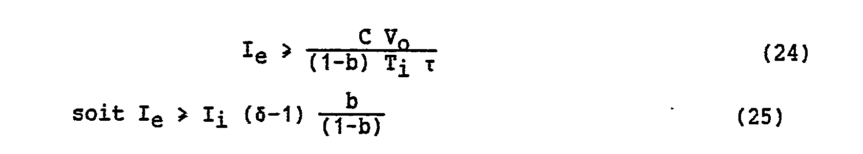
I e = CV o / n T r τ (22ʹ)
(n = number of scan lines per image, T r = line feed duration), this erase duration T e is at most equal to the blanking duration, that is:
T e ≦ (1-b) T i (23)
In that case :
Dans l'exemple choisi avec une cible de 240 µm d'épaisseur, on obtient Ie = 500 µA.In the example chosen with a 240 µm thick target, I e = 500 µA is obtained.
La disproportion entre les courants nécessaires à l'effacement et à l'inscription peut être sensiblement réduite en modifiant le taux de blanking b. En effet, si on utilise un circuit électronique de désentrelacement des lignes, tel que celui décrit ci-après, il est possible de modifier le débit des signaux pour réduire la durée de l'inscription et allonger d'autant la durée de l'effacement.The disproportion between the currents necessary for erasure and registration can be significantly reduced by modifying the blanking rate b. In fact, if an electronic deinterlacing circuit of the lines is used, such as that described below, it is possible to modify the signal rate to reduce the duration of the recording and lengthen the duration of the erasure accordingly. .
Les tableaux ci-après donnent les durées, les courants à l'inscription et à l'effacement ainsi que la bande passante du signal vidéo pour différentes valeurs du blanking b dans les standards 625 et 1023 lignes TV.

Le tranage est nul en accumulation de charges. En effet, avant chaque inscription, il y a effacement total de l'image précédente et, par conséquent, il n'y a pas d'empilement des résidus des images précédentes.Tranage is zero in accumulation of charges. Indeed, before each registration, there is total erasure of the previous image and, therefore, there is no stacking of the residues of the previous images.
Le mode ACC présente plusieurs avantages : en effet, la distance grille-cible ne joue aucun rôle sur la résolution d'image, par conséquent la grille peut être montée à 0,5 mm, voire à plusieurs millimètres, de distance de la cible. La force électrostatique entre la cible et la grille est réduite d'un facteur 10² à 10³ et l'ombre de la grille est considérablement atténuée.The ACC mode has several advantages: in fact, the grid-target distance does not play any role on the image resolution, therefore the grid can be mounted 0.5 mm or even several millimeters away from the target. The electrostatic force between the target and the grid is reduced by a factor of 10² to 10³ and the shadow of the grid is considerably reduced.
On élimine ainsi des difficultés :
- de fabrication et de montage mécanique de la grille,
- de tenue en tension de cette grille,
- de résistance de couche conductrice transparente,
- de moiré entre fréquence spatiale de la mire et fréquence spatiale des fils de grille.This eliminates difficulties:
- manufacturing and mechanical assembly of the grid,
- voltage resistance of this grid,
- resistance of transparent conductive layer,
- moiré between spatial frequency of the target and spatial frequency of the grid wires.
Il n'apparaît plus de relation entre la limite de résolution et le nombre de fils de grille. Il y a suppression de la surmodulation des contours et des aigrettes, ce qui améliore la lisibilité des caractères et rend l'image plus confortable.There no longer appears a relationship between the resolution limit and the number of grid wires. The over-modulation of outlines and crests has been eliminated, which improves the readability of the characters and makes the image more comfortable.
En accumulation de charges l'amplificateur vidéo module le wehnelt (environ 60 volts sur 8 pF) au lieu de la cible (150 V sur 400 pF) en stabilisation de potentiel.In charge accumulation the video amplifier modulates the wehnelt (around 60 volts on 8 pF) instead of the target (150 V on 400 pF) in potential stabilization.
Pour effacer la cible on utilise un effacement précurseur appelé ainsi parce qu'il précède l'écriture et porte sur quelques lignes situées au-delà de la ligne en cours d'écriture.To erase the target we use a precursor erase called so because it precedes writing and relates to a few lines located beyond the line being written.
Il est souhaitable que l'effacement soit plus large que l'inscription à condition de ne pas affecter la ligne que l'on vient d'écrire, c'est-à-dire à condition d'effectuer l'effacement en avance de quelques lignes sur celle à écrire.It is desirable for the erasure to be wider than the entry provided that the line just written is not affected, that is to say provided that the erasure is carried out in advance by a few lines on the one to write.
Soit n le numéro de la ligne à écrire. On fera l'effacement préférentiellement pendant chaque retour de balayage avec un courant I x 10 qui va s'étaler par exemple sur q = 10 lignes et concerner les lignes de rang n+2 à n+12. Le spot décrit indéfiniment des boucles rectangulaires de la hauteur de 7 lignes, qui balayent l'écran de haut en bas à la vitesse de balayage trame.Let n be the number of the line to write. We will do the erasure preferably during each sweep return with a current I x 10 which will spread for example over q = 10 lines and concern the lines of rank n + 2 to n + 12. The spot indefinitely describes rectangular loops the height of 7 lines, which scan the screen from top to bottom at the frame scanning speed.
La luminosité reste à peu près inchangée car la bande noire qui précède l'inscription occupe, dans cet exemple, une hauteur maximale de 12 lignes si l'image est très sombre et de 2 lignes s'il s'agit d'une image très lumineuse soit, dans tous les cas, une perte de niveau lumineux inférieure à 12/625 ≃ 2 %. Le papillotement est imperceptible.The brightness remains almost unchanged because the black band preceding the inscription occupies, in this example, a maximum height of 12 lines if the image is very dark and 2 lines if it is a very light or, in all cases, a loss of light level less than 12/625 ≃ 2%. The flicker is imperceptible.
Mais pour ne pas effacer simultanément les lignes paires et impaires, ce qui produirait une diminution de la luminosité par rapport au mode à stabilisation de potentiel, il y a lieu de supprimer l'entrelacement des lignes de balayage. S'il s'agit d'un système de télévision en circuit fermé, la caméra de prise de vue peut être modifée spéciale ment pour délivrer un signal vidéo non entrelacé. Ceci est également vrai pour un générateur d'images synthétisées par ordinateur. Les standards de TV existants fonctionnant avec entrelacement, il faut transformer les standards et faire que toutes les lignes par exemple 625 lignes, soient jointives et défilent au cours d'une seule trame de 40 ms.However, in order not to erase the even and odd lines simultaneously, which would produce a reduction in brightness compared to the potential stabilization mode, it is necessary to remove the interlacing of the scanning lines. In the case of a closed circuit television system, the camera can be specially modified to deliver a non-interlaced video signal. This is also true for a computer synthesized image generator. The existing TV standards working with interleaving, it is necessary to transform the standards and make that all the lines for example 625 lines, are contiguous and scroll in the course of a single frame of 40 ms.
Par conséquent, ce mode de fonctionnement avec effacement précurseur nécessite un convertisseur de standard entrelacé en standard non entrelacé.Consequently, this operating mode with precursor erasure requires an interleaved standard to non-interlaced standard converter.
Pour effectuer cette conversion de standard, préférentiellement on utilise une mémoire d'image de grande capacité mémoire.To carry out this standard conversion, preferably a large memory image memory is used.
Le circuit de désentrelacement a pour rôle de reclasser chacune des 312,5 lignes de rang impair (trame impaire) et des 312,5 lignes de rang pair (trame paire) de façon à reconstituer une image entière où les 625 lignes défilent régulièrement les unes après les autres en une seule séquence de 40 ms. Il est donc nécessaire d'avoir emmagasiné la totalité des deux trames avant d'effectuer le reclassement et, s'il s'agit de mémoires à accès séquentiel, il faudra deux blocs de mémoire d'image qui seront alternativement en chargement et en lecture.The role of the deinterlacing circuit is to reclassify each of the 312.5 lines of odd rank (odd frame) and of the 312.5 lines of even rank (even frame) so as to reconstitute an entire image where the 625 lines pass regularly through one after the others in a single sequence 40 ms. It is therefore necessary to have stored all of the two frames before performing the reclassification and, in the case of sequential access memories, two blocks of image memory will be required which will be alternately loading and reading. .
Par exemple, si l'on veut mémoriser une image de 1200 P/L x 100 lignes numérisées sur 8 bits, cela conduit à 9,6.10+6 bits. Pour effectuer le désentrelacement avec une mémoire à accès séquentiel, il faut une capacité mémoire de 1,92.10+7 bits. Les mémoires à circuits intégrés à dispositifs à transfert de charges de 300 kbits par boîtier, permettent de réaliser cette opération.For example, if you want to store an image of 1200 P / L x 100 lines scanned on 8 bits, this leads to 9.6.10 +6 bits. To perform deinterlacing with sequential access memory, a memory capacity of 1.92.10 + 7 bits is required. The memories with integrated circuits with charge transfer devices of 300 kbits per box, make it possible to carry out this operation.
L'invention sera mieux comprise à l'aide des figures suivantes, données à titre d'exemples non limitatifs, qui représentent :
- figure 1 : une coupe de la partie essentielle du relais optique selon l'art antérieur,
- figure 2 : un schéma-bloc représentant les moyens pour faire fonctionner le relais optique en accumulation de charges et un compteur pour effectuer l'effacement précurseur,
- figure 3 : un schéma-bloc analogue à celui de la figure 2 avec en plus une mémoire d'image pour effectuer le désentrelacement d'un standard de télévision,
- figure 4 : une représentation du mode d'écriture et du mode d'effacement précurseur d'une trame selon l'invention,
- figure 5 : un schéma-bloc d'un exemple de mémoire d'images opérant le désentrelacement.
- FIG. 1: a section of the essential part of the optical relay according to the prior art,
- FIG. 2: a block diagram representing the means for operating the optical relay in accumulation of charges and a counter for erasing the precursor,
- FIG. 3: a block diagram similar to that of FIG. 2 with in addition an image memory for performing the deinterlacing of a television standard,
- FIG. 4: a representation of the writing mode and the precursor erasure mode of a frame according to the invention,
- FIG. 5: a block diagram of an example of image memory operating the deinterlacing.
Sur la figure 1, sont schématiquement représentés, les organes essentiels d'un relais optique conforme à l'invention, et ceux qui coopèrent avec ce relais à l'obtention d'une image visible, projetée sur un écran 2 par une lentille de projection 4. La lumière est fournie par une lampe 6, représentée comme étant à incandescence, mais qui pourrait évidemment être de tout autre type. Cette lumière traverse une lentille de collimation 8, puis une cuve 10 dont le rôle est d'arrêter le rayonnement calorifique infrarouge. Le relais optique est essentiellement constitué par une cible 12, formée d'un monocristal parallélépipédique de KDP dont l'axe optique (c) est perpendiculaire aux grandes faces, et placée entre les deux polariseurs croisés 14 et 16 dont les plans de polarisation sont parallèles aux deux autres axes cristallographiques (a et b) du monocristal. Un échangeur thermique 18 est en contact avec la cible 12 et la maintient au voisinage de sa température de Curie. La face gauche de cette cible reçoit un faisceau d'électrons, représenté en pointillé et issu d'un canon à électrons 20. Ce faisceau balaye périodiquement toute la surface utile de la cible 12 sous l'action d'organes de déflexion 22 commandés par les signaux de balayage issus d'un récepteur 24 qui les élabore à partir des signaux de synchro nisation qui lui sont fournis à son entrée 26 avec le signal d'information visuelle proprement dit. Un bloc 28 fournit à certains des organes déjà cités les tensions électriques continues qui leur sont nécessaires, ainsi qu'à une anode 30. Ce n'est que pour la clarté du dessin que celle-ci est représentée sous la forme d'une plaque parallèle au faisceau lumineux, car il est évident que cette disposition, très favorable au passage de la lumière ne l'est guère à la collection des électrons secondaires émis par tous les points de la surface de la cible 12 atteints par le faisceau électronique. C'est pourquoi, dans la pratique, l'anode est disposée parallèlement à la surface de la cible 12 et tout près de celle-ci. Comme elle doit être traversée par le faisceau d'électrons incidents et par la lumière, on lui donne une forme appropriée, celle d'une grille par exemple. Une lame 38 électriquement conductrice et optiquement transparente, à l'aide d'une mince couche d'or par exemple, est disposée derrière la cible 12. C'est à cette lame que le récepteur 24 applique le signal d'information visuelle.In Figure 1, are schematically represented, the essential organs of an optical relay according to the invention, and those which cooperate with this relay to obtain a visible image, projected on a screen 2 by a projection lens 4. The light is supplied by a lamp 6, shown as being incandescent, but which could obviously be of any other type. This light crosses a collimating lens 8, then a tank 10 whose role is to stop infrared heat radiation. The optical relay is essentially constituted by a
La figure 2 représente des éléments essentiels 27 du relais optique décrit sur la figure 1. Le canon à élec trons 20 est ici symbolisé par une cathode. Les moyens de fonctionnement 23 permettent de faire fonctionner le relais optique en mode d'accumulation de charges. Pour cela, en mode écriture, les moyens de fonctionnement 23 appliquent sur le wehnelt 25 le signal de modulation de polarité négative issu d'un générateur vidéo symbolisé par une antenne 60. La polarisation continue du wehnelt est par exemple de -600 volts et la modulation superposée est par exemple de -100 volts crête. Le dispositif de déflexion de faisceau 22 opère de sorte que le canon à électrons 20 écrit sur la n-ième ligne de la trame. Les moyens 23 appliquent simultanément une polarisation continue de -250 volts sur la lame 38 placée derrière la cible 12. En mode d'effacement le faisceau d'électrons est défléchi par le dispositif 22 pour atteindre la (n+p)ième ligne, par exemple n+7. Simultanément le courant délivré par le canon 20 est augmenté par les moyens 23 en supprimant la modulation du wehnelt.FIG. 2 represents
Dans les deux cas la grille-anode 30 est au potentiel de la masse. La détermination de la (n+p)ième ligne est effectuée par le compteur de lignes 61 qui commande en conséquences les moyens 23. En mode d'effacement la lame 38 est portée au potentiel de la masse. Lorsque les informations à représenter sur l'écran nécessitent une échelle de gris, ou de demi-teintes, par exemple lorsqu'ils ne sont pas constitués de caractères alphanumériques mais par des images représentant des personnages, il est alors souhaitable d'utiliser une grille auxiliaire de focalisation 29 qui reçoit une partie du signal vidéo appliqué au wehnelt 25.In both cases the
Le schéma de la figure 2 s'applique au cas où le signal vidéo qui arrive du générateur vidéo ne correspond pas à un signal entrelacé comme cela peut être le cas avec des caméras adaptées ou des circuits internes de diffusion.The diagram in FIG. 2 applies to the case where the video signal arriving from the video generator does not correspond to an interlaced signal as may be the case with suitable cameras or internal broadcasting circuits.
La figure 3 s'applique au cas général des standards de télévision qui sont généralement entrelacés. Pour appliquer l'effacement précurseur il est souhaitable, afin de ne pas perdre en luminosité d'image, d'effectuer un désentrelacement préalable. Ceci est effectué dans le dispositif de désentrelacement 35 qui reçoit le signal vidéo de l'antenne 60. Ce dispositif de désentrelacement délivre un signal vidéo désentrelacé qui est appliqué sur le wehnelt 25 à travers les moyens 23. Les autres éléments sont représentés avec les mêmes repères que sur la figure 2.Figure 3 applies to the general case of television standards which are generally interleaved. To apply the precursor erasure it is desirable, in order to do not lose image brightness, perform a prior deinterlacing. This is done in the
La figure 4 représente le mode d'écriture et le mode d'effacement précurseur d'une trame selon l'invention. Ceci est indiqué pour un exemple de trame à 625 lignes. Lorsque le faisceau d'électrons a fini d'écrire la n-ième ligne, les moyens de déflexion le font passer à la (n+p)ième ligne, par exemple n+7. Il décrit alors la (n+7)ième ligne en retour de lignes. Lorsque cette (n+7)ième ligne a été balayée, il est défléchi sur la (n+1)ième ligne et repasse en mode d'écriture. Selon ce dernier mode le profil du courant de faisceau est représenté sous le repère 41. C'est un courant de faisceau très focalisé sur la n-ième ligne, de valeur par exemple Ie = 59 microampères. En mode d'effacement le faisceau est largement défocalisé de sorte qu'il arrose un nombre élevé de lignes, mais sans jamais atteindre la n-ième ligne qui vient d'être écrite. L'effacement s'effectue ainsi environ de la (n+2)ième ligne à la (n+12)ième ligne par exemple. Le profil du courant de faisceau est représenté sous le repère 42. La valeur de ce courant d'effacement est beaucoup plus élevée par exemple 500 microampères.FIG. 4 represents the writing mode and the precursor erasing mode of a frame according to the invention. This is shown for an example frame with 625 lines. When the electron beam has finished writing the n-th line, the deflection means pass it to the (n + p) th line, for
Le repère 43 indique les lignes de l'image nouvelle qui viennent d'être écrites et le repère 44 les lignes de l'image précédente qui n'ont pas encore été effacées.The
La figure 5 représente un dispositif de désentrelacement 35. Lorsque le signal est issu d'une antenne 60, il est détecté par un détecteur 50 puis filtré par un filtre 51. Cette opération disparaît si le signal est délivré sous la forme d'un signal vidéo issu d'un générateur vidéo. Le signal vidéo est numérisé par un convertisseur analogique-numérique 52. Le signal numérique est aiguillé par un commutateur 53 alternativement selon deux voies 54₁ et 54₂. L'alternance se fait au rythme de la durée d'une trame par exemple 40 ms. Le signal entrelacé des voies 54₁ et 54₂ est désentrelacé respectivement à l'aide des commutateurs 55₁ et 55₂ qui sélectionnent successivement les lignes paires et impaires de chaque trame. Cette sélection s'effectue au rythme de chaque demi-trame soit dans l'exemple 20 ms.FIG. 5 represents a
Ainsi toutes les lignes impaires 1, 3, 5, ... sont stockées dans les mémoires 56₁ et 56₂ pour respectivement les voies 54₁ et 54₂, et toutes les lignes paires 2, 4, 6, ... sont stockées dans les mémoires 57₁ et 57₂ pour respectivement les voies 54₁ et 54₂. Pour désentrelacer chaque voie les commutateurs 58₁ et 58₂ vont alternativement sélectionner les lignes paires et les lignes impaires au rythme de la durée d'une ligne, par exemple 64 microsecondes, pour obtenir sur les voies de sortie 59₁ et 59₂ les lignes désentrelacées apparaissant dans l'ordre 1, 2, 3, 4, 5, .... Les blocs mémoire 56₁ et 57₁ d'une part, et les blocs 56₂ et 57₂ d'autre part opèrent en alternance de sorte que les uns sont chargés lorsque les autres sont lus. Cette sélection est effectuée à l'aide du commutateur 65. Le signal numérique est reconverti en analogique à l'aide d'un convertisseur numérique-analogique 66 puis filtré par un filtre 67 pour être utilisé.Thus all the
Claims (6)
- un commutateur de demi-trame qui oriente alternativement chaque demi-trame vers deux mémoires stockant respectivement la trame impaire et la trame paire, puis un commutateur de lignes sélectionnant alternativement les lignes d'ordre pair et d'ordre impair afin de construire une trame désentrelacée,
chaque trame désentrelacée des deux voies étant alternativement sélectionnée par un commutateur de trame qui permet d'effectuer la lecture d'une des voies tandis que l'autre est en cours de chargement et inversement, le signal sélectionné étant reconverti en signal analogique à l'aide d'un convertisseur numérique-analogique puis filtré à l'aide d'un filtre pour fournir un signal vidéo désentrelacé.6. Optical relay according to claim 5, characterized in that the conversion device comprises an analog-digital converter which operates on the interlaced video signal, a frame switch, alternately orienting each frame of the interlaced signal on two channels, each of these tracks including:
- a half-frame switch which alternately directs each half-frame to two memories storing respectively the odd frame and the even frame, then a line switch alternately selecting the lines of even order and odd order in order to build a frame deinterleaved,
each deinterlaced frame of the two channels being alternately selected by a frame switch which makes it possible to read one of the channels while the other is in during loading and vice versa, the selected signal being reconverted into analog signal using a digital-analog converter then filtered using a filter to provide a deinterlaced video signal.
Applications Claiming Priority (2)
| Application Number | Priority Date | Filing Date | Title |
|---|---|---|---|
| FR8602993A FR2595496B1 (en) | 1986-03-04 | 1986-03-04 | OPTICAL RELAY OPERATING IN CHARGE ACCUMULATION MODE |
| FR8602993 | 1986-03-04 |
Publications (1)
| Publication Number | Publication Date |
|---|---|
| EP0240043A1 true EP0240043A1 (en) | 1987-10-07 |
Family
ID=9332728
Family Applications (1)
| Application Number | Title | Priority Date | Filing Date |
|---|---|---|---|
| EP87200320A Ceased EP0240043A1 (en) | 1986-03-04 | 1987-02-25 | Optical relay operating in a charge accumulation mode |
Country Status (5)
| Country | Link |
|---|---|
| US (1) | US4800436A (en) |
| EP (1) | EP0240043A1 (en) |
| JP (1) | JPS62235920A (en) |
| DK (1) | DK103187A (en) |
| FR (1) | FR2595496B1 (en) |
Families Citing this family (10)
| Publication number | Priority date | Publication date | Assignee | Title |
|---|---|---|---|---|
| US6269484B1 (en) | 1997-06-24 | 2001-07-31 | Ati Technologies | Method and apparatus for de-interlacing interlaced content using motion vectors in compressed video streams |
| DE19749331A1 (en) * | 1997-11-07 | 1999-05-20 | Kostal Leopold Gmbh & Co Kg | Method of detecting objects on motor vehicle windscreen |
| US7483577B2 (en) * | 2004-03-02 | 2009-01-27 | Mitsubishi Electric Research Laboratories, Inc. | System and method for joint de-interlacing and down-sampling using adaptive frame and field filtering |
| US8115863B2 (en) * | 2007-04-04 | 2012-02-14 | Freescale Semiconductor, Inc. | Video de-interlacer using pixel trajectory |
| US8964117B2 (en) * | 2007-09-28 | 2015-02-24 | Ati Technologies Ulc | Single-pass motion adaptive deinterlacer and method therefore |
| US8300987B2 (en) * | 2007-09-28 | 2012-10-30 | Ati Technologies Ulc | Apparatus and method for generating a detail-enhanced upscaled image |
| US8259228B2 (en) * | 2007-12-10 | 2012-09-04 | Ati Technologies Ulc | Method and apparatus for high quality video motion adaptive edge-directional deinterlacing |
| US8396129B2 (en) * | 2007-12-28 | 2013-03-12 | Ati Technologies Ulc | Apparatus and method for single-pass, gradient-based motion compensated image rate conversion |
| RU2013126525A (en) * | 2010-11-09 | 2014-12-20 | ЛОРЕНС ЛИВЕРМОР НЭШНЛ СЕКЬЮРИТИ, ЭлЭлСи | MULTI-CRYSTAL FREQUENCY MOTOR FOR CONVERSION TO THIRD HARMONIC |
| EP2704427A1 (en) * | 2012-08-31 | 2014-03-05 | Axis AB | Method and apparatus for de-interlacing video |
Citations (1)
| Publication number | Priority date | Publication date | Assignee | Title |
|---|---|---|---|---|
| US3637931A (en) * | 1968-12-20 | 1972-01-25 | Philips Corp | Optic relay for use in television |
Family Cites Families (5)
| Publication number | Priority date | Publication date | Assignee | Title |
|---|---|---|---|---|
| FR1479264A (en) * | 1965-12-09 | 1967-05-05 | Pompey Acieries | Improvements to casting ladles |
| FR1479284A (en) * | 1966-01-26 | 1967-05-05 | Electronique & Physique | Optical relay, especially for television projectors |
| FR1473212A (en) * | 1966-01-26 | 1967-03-17 | Electronique & Physique | Optical relay applicable to television |
| US3723651A (en) * | 1971-12-27 | 1973-03-27 | Rca Corp | Optically-scanned liquid-crystal projection display |
| US4611235A (en) * | 1984-06-04 | 1986-09-09 | General Motors Corporation | Thyristor with turn-off FET |
-
1986
- 1986-03-04 FR FR8602993A patent/FR2595496B1/en not_active Expired
-
1987
- 1987-02-25 EP EP87200320A patent/EP0240043A1/en not_active Ceased
- 1987-02-27 DK DK103187A patent/DK103187A/en not_active Application Discontinuation
- 1987-03-02 US US07/020,923 patent/US4800436A/en not_active Expired - Fee Related
- 1987-03-04 JP JP62047852A patent/JPS62235920A/en active Pending
Patent Citations (1)
| Publication number | Priority date | Publication date | Assignee | Title |
|---|---|---|---|---|
| US3637931A (en) * | 1968-12-20 | 1972-01-25 | Philips Corp | Optic relay for use in television |
Non-Patent Citations (1)
| Title |
|---|
| 1985 SID INTERNATIONAL SYMPOSIUM DIGEST OF TECHNICAL PAPERS, Society for SID Information Display, 1ère édition, mai 1985, pages 266-269, Palisades Institute for Research Services, Inc., New York, US; A. FARRAYRE et al.: "14.4: Geometrical resolution improvement of sodern visualization system" * |
Also Published As
| Publication number | Publication date |
|---|---|
| FR2595496A1 (en) | 1987-09-11 |
| US4800436A (en) | 1989-01-24 |
| DK103187A (en) | 1987-09-05 |
| DK103187D0 (en) | 1987-02-27 |
| JPS62235920A (en) | 1987-10-16 |
| FR2595496B1 (en) | 1988-05-06 |
Similar Documents
| Publication | Publication Date | Title |
|---|---|---|
| EP0327236B1 (en) | Image pickup apparatus | |
| US4945423A (en) | Reproducing apparatus for charge latent image recording medium | |
| US2276359A (en) | Television image projection device | |
| EP0240043A1 (en) | Optical relay operating in a charge accumulation mode | |
| FR2507802A1 (en) | LIQUID CRYSTAL DISPLAY DEVICE HAVING TWO ADDRESSING MODES | |
| US4956713A (en) | Image pick-up apparatus using photo-to-photo conversion element | |
| Salvo | Solid-state light valve | |
| CA1332465C (en) | Method and apparatus of repeatedly recording optical image information and image pickup device | |
| Donjon et al. | A Pockels-effect light valve: Phototitus. Applications to optical image processing | |
| FR2528588A1 (en) | METHOD AND DEVICE FOR COMPOSING AND RECAPING MULTIPLE ELECTRONIC IMAGES ON A PHOTOSENSITIVE SURFACE | |
| WO1992008160A1 (en) | Apparatus for and method of operation of smectic liquid crystal light valve | |
| EP0217455B1 (en) | Optical relay with the target plate operating in the ferroelectric state | |
| US3702215A (en) | Electron beam controlled bistable ferroelectric light valve | |
| KR930000514B1 (en) | Optical information recording material and recording/play-back system | |
| EP0237107A1 (en) | Optical relay for generating a projected picture having characters with improved legibility | |
| EP0376282B1 (en) | Photo-modulation method and system for reproducing charge latent image | |
| FR2645322A1 (en) | ELECTRO-OPTICAL MEMORY DEVICE WITH LIQUID CRYSTALS | |
| US5031047A (en) | Image information processing method and apparatus thereof | |
| EP0270167A1 (en) | Optical relay in which the target is cooled by a heat exchanger with a controlled-temperature gradient | |
| JPH0787555B2 (en) | Imaging device | |
| JPH04277716A (en) | Information recording medium and information recording device | |
| JPH01286685A (en) | Image pickup device | |
| JPH0229173A (en) | Method for recording and reproducing electrostatic latent image | |
| Motoki et al. | Direct Laser-Beam Recording of Color Television Signals on Color Print Film | |
| JPH0715751A (en) | Holography television |
Legal Events
| Date | Code | Title | Description |
|---|---|---|---|
| PUAI | Public reference made under article 153(3) epc to a published international application that has entered the european phase |
Free format text: ORIGINAL CODE: 0009012 |
|
| AK | Designated contracting states |
Kind code of ref document: A1 Designated state(s): DE FR GB IT |
|
| 17P | Request for examination filed |
Effective date: 19880402 |
|
| RAP1 | Party data changed (applicant data changed or rights of an application transferred) |
Owner name: N.V. PHILIPS' GLOEILAMPENFABRIEKEN Owner name: LABORATOIRES D'ELECTRONIQUE PHILIPS |
|
| 17Q | First examination report despatched |
Effective date: 19900702 |
|
| STAA | Information on the status of an ep patent application or granted ep patent |
Free format text: STATUS: THE APPLICATION HAS BEEN REFUSED |
|
| 18R | Application refused |
Effective date: 19901227 |
|
| RIN1 | Information on inventor provided before grant (corrected) |
Inventor name: SCHORTER, BRUNO Inventor name: POLAERT, REMY |