EP0239352A2 - Phased array semiconductor lasers - Google Patents
Phased array semiconductor lasers Download PDFInfo
- Publication number
- EP0239352A2 EP0239352A2 EP87302498A EP87302498A EP0239352A2 EP 0239352 A2 EP0239352 A2 EP 0239352A2 EP 87302498 A EP87302498 A EP 87302498A EP 87302498 A EP87302498 A EP 87302498A EP 0239352 A2 EP0239352 A2 EP 0239352A2
- Authority
- EP
- European Patent Office
- Prior art keywords
- laser
- elements
- laser elements
- supermode
- array
- Prior art date
- Legal status (The legal status is an assumption and is not a legal conclusion. Google has not performed a legal analysis and makes no representation as to the accuracy of the status listed.)
- Granted
Links
- 239000004065 semiconductor Substances 0.000 title claims abstract description 9
- 230000003287 optical effect Effects 0.000 claims abstract description 32
- 230000008878 coupling Effects 0.000 claims abstract description 24
- 238000010168 coupling process Methods 0.000 claims abstract description 24
- 238000005859 coupling reaction Methods 0.000 claims abstract description 24
- 238000005086 pumping Methods 0.000 description 10
- 230000005855 radiation Effects 0.000 description 4
- 239000011159 matrix material Substances 0.000 description 3
- 238000012986 modification Methods 0.000 description 2
- 230000004048 modification Effects 0.000 description 2
- 239000000243 solution Substances 0.000 description 2
- 238000004458 analytical method Methods 0.000 description 1
- 238000003491 array Methods 0.000 description 1
- 238000010276 construction Methods 0.000 description 1
- 230000006866 deterioration Effects 0.000 description 1
- 238000009792 diffusion process Methods 0.000 description 1
- 238000002347 injection Methods 0.000 description 1
- 239000007924 injection Substances 0.000 description 1
- 230000003993 interaction Effects 0.000 description 1
- 230000006798 recombination Effects 0.000 description 1
- 238000005215 recombination Methods 0.000 description 1
- 230000006641 stabilisation Effects 0.000 description 1
- 238000011105 stabilization Methods 0.000 description 1
- 230000000087 stabilizing effect Effects 0.000 description 1
Images

Classifications
-
- H—ELECTRICITY
- H01—ELECTRIC ELEMENTS
- H01S—DEVICES USING THE PROCESS OF LIGHT AMPLIFICATION BY STIMULATED EMISSION OF RADIATION [LASER] TO AMPLIFY OR GENERATE LIGHT; DEVICES USING STIMULATED EMISSION OF ELECTROMAGNETIC RADIATION IN WAVE RANGES OTHER THAN OPTICAL
- H01S5/00—Semiconductor lasers
- H01S5/40—Arrangement of two or more semiconductor lasers, not provided for in groups H01S5/02 - H01S5/30
- H01S5/4025—Array arrangements, e.g. constituted by discrete laser diodes or laser bar
- H01S5/4031—Edge-emitting structures
Definitions
- This invention relates to phased array semiconductive lasers having multi-emission or broad emission capabilities and in particular to phased array lasers having structural design that maintains their operation in a preferred stable supermode pattern.
- Phased array semiconductor lasers comprise a plurality of spaced emitters on the same wafer. Examples of such phased array lasers are illustrated in U.S. Patent No. 4,255,717, now Reissue Patent 31,806 issued January 15, 1985, and in an article of William Streifer et al, entitled “Phased Array Diode Lasers", published in the June 1984 Issue of Laser Focus/Electro-Optics.
- the emitters of such a laser are confined by the periodically spaced current confinement means, e.g. stripes, for current pumping and establishment of spaced optical filaments in the active region of the structure or by internal waveguide structuring.
- the current confinement means may be interconnected or the emitters closely spaced to a degree that the optical mode established in each of the filaments couples to neighboring optical filament modes, i.e., the evanescent wave overlaps into adjacent optical lasing cavities.
- the array of optical fields produced become phased locked, and, if the phase difference between adjacent current confinement means is zero, the lateral radiation pattern in the far field will comprise a single lobe.
- the phased array laser does not operate to radiate in a single lobe but rather generally operates with radiation in two or more lobes in the far field pattern.
- the phase relationship between adjacent optical filaments is not under control and the phases themselves adjust in a manner to minimize laser threshold current.
- phased array semiconductor lasers with N coupled single mode waveguides may lase in any one of N supermodes or array modes.
- the term "supermode" has reference to the superposition behavior of a particular field amplitude pattern across the array. Most of these devices tend to lase in the highest order N th supermode, which radiates in a twin lobe far field pattern, whereas the 1st supermode is optimum for applications in that its radiation pattern is a single lobe. Much attention has been devoted in the past few years to fabricating arrays favoring the 1st supermode, by minimizing its threshold relative to the other supermodes.
- An array laser with N coupled emitters has N possible coupled array modes or supermodes.
- a supermode is a cooperative lasing of the N optical emitters or filaments of the array laser. Since there are N emitters, there are N possible supermodes since all these emitters are optically coupled together.
- Each supermode has the property that the 1st and the N th supermode have the same intensity pattern or envelope, the 2 nd and the N-1 th have the same intensity envelope, and, in general, the i th and N + 1-i th have the same intensity envelopes.
- the 1 st or fundamental supermode has all emitters lasing in phase with an amplitude distribution representative of half a sinusoidal cycle. This is the only supermode pattern that radiates in a single central lobe in the far field pattern because all emitters radiate in phase.
- the envelope of the intensity pattern is very similar to the envelope intensity pattern shown for the 1st supermode in Figure 1A except that alternating emitters have alternating phase, i.e. are out of phase by ⁇ . As a result, this supermode will radiate in two fairly symmetrical lobes in the far field pattern.
- the supermode field amplitude pattern 20 for the 2nd supermode is shown in Figure 1C wherein the envelope 22 across the array is sinusoidal comprising one positive half cycle and one negative half cycle.
- the 2 nd supermode will lase in two closely space symmetrical lobes in the far field pattern.
- the 1 st and N th supermode intensity envelopes are half a sinusoidal period
- the 2 nd and the N-1 th supermode intensity envelopes are two half sinusoidal periods, etc.
- the phases of the individual emitters in the 1 st and N th supermodes differ. Specifically, for the 1 st supermode, all emitters are in phase and for the N th supermode, the phases alternate between zero and ⁇ .
- the 1 st and Nth supermodes have the lowest current thresholds as compared to all other supermodes because their intensity envelopes do not exhibit nulls near the center of the array where the charge density is greater as a result of current spreading and charge diffusion in the active region of the array laser.
- the N th supermode which radiates in two lobes, has a lower current threshold of operation than the 1 st supermode due to the lower gain which naturally occurs between emitting regions.
- the primary reason for supermode instability above threshold is the incomplete utilization of the injected charges with increased pumping.
- the envelope of the individual modal field amplitudes is sinusoidal for all the supermodes and is a half cycle for the 1 st and N th supermodes as shown in Figures 1A and 1B.
- An estimation of the sine envelope squared intensity pattern overlap with the fairly rectangular shaped charge distribution pattern 14 indicates that only about 50% of the injected charges will be stimulated to recombine above threshold by any single supermode. Therefore, at best, with a single supermode lasing, the differential efficiency will be reduced by that factor.
- the excess charges will provide excess gain, which will encourage other supermodes to lase, thereby producing a deterioration in the far field radiation pattern.
- a phased array semiconductor laser favoring emission in the 1 st or N th supermode over other potential supermodes of the laser comprises a plurality of spatially disposed laser elements formed relative to an active region to provide optical cavities for light wave generation and propagation under lasing conditions and wherein the optical field of said laser elements are coupled into the optical cavities of adjacent laser elements to provide a phase locked condition across the array.
- the position of the outer laser element at each end of the array are spaced closer to its adjacent laser element compared to the spacing provided between the other laser elements such that its coupling is enhanced to produce one or more supermodes with an intensity envelope which for its most part is substantially uniform and rectangular-shaped.
- the optical coupling coefficient between the outer laser elements and their adjacent laser elements is ⁇ 2 K where K is the optical coupling coefficient between the other equally spaced laser elements.
- the general construction and structure of array laser 30 is well known in the art as illustrated in the aforementioned Reissue Patent 31,806 and the above mentioned article of William Streifer et al.
- Laser elements 33-40 of laser 30 are mutually separated by a space, D.
- the outside laser elements 32 and 41 of array laser 30 are more closely spaced to their adjacent laser elements 33 and 40 as indicated by the spacing D.
- the closer spacing of outer laser elements 32 and 41 provides for more overlaps of the evanescent wave into the adjacent optical lasing cavities of neighboring laser elements 33 and 40.
- the envelopes 44 and 46 of modal field amptitudes respectively for the 1 st and N th supermodes shown in Figures 3 and 4 are almost rectangular in shape and are very similar in shape to the charge distribution pattern 14 in Figure 1.
- the substantially uniform utilization of charge injection across most of the array will bring about stabilization of either the 1 st or N th supermode array in array laser 30, i.e. the supermode preferred will be relatively stable with increasing current pumping above lasing threshold.
- the field intensities of the individual laser elements will be approximately equal in all or most of the waveguides of the laser elements with the exception of the outer most waveguides of the outer most laser elements, which are at an inensity of 1/ ⁇ 2 compared to the remaining laser elements.
- all or most all of the laser elements will be in phase with the exception that in some of the laser elements, the phase may be purposely reversed to shape or otherewise control the far field pattern.
- this is the 180° phase reversal of laser elements 33, 35, 37, 39, and 41 in Figure 4 to produce an envelope substantially the same as that shown in Figure 3 for the 1 st supermode.
- the matrix M differs from the one describing a uniform array only in the presence of ⁇ 2 K at the extremes of the diagonals.
- an array of identical laser elements can be designed such that the 1 st and N th supermodes have equal intensities in all but the waveguides in the outermost laser elements.
- Laser elements 2 through N-1 are equally spaced and coupled; laser elements 1 and N are placed more closely to their neighboring elements such that their coupling coefficients are greater by a factor of ⁇ 2.
- the 1 st and N th supermodes have uniform field strengths, except in the waveguides of the outermost laser elements 1 and N wherein the field is weaker by 1/ ⁇ 2. Because these supermodes have maximum overlap with the injected charge distribution, their thresholds are lower than the other supermodes. Furthermore, above threshold, these supermodes more efficiently utilize the injected charges so that other supermodes are not encouraged to begin lasing and the single lasing mode is stable over varied current pumping range.
Landscapes
- Physics & Mathematics (AREA)
- Condensed Matter Physics & Semiconductors (AREA)
- General Physics & Mathematics (AREA)
- Electromagnetism (AREA)
- Optics & Photonics (AREA)
- Semiconductor Lasers (AREA)
Abstract
Description
- This invention relates to phased array semiconductive lasers having multi-emission or broad emission capabilities and in particular to phased array lasers having structural design that maintains their operation in a preferred stable supermode pattern.
- Phased array semiconductor lasers comprise a plurality of spaced emitters on the same wafer. Examples of such phased array lasers are illustrated in U.S. Patent No. 4,255,717, now Reissue Patent 31,806 issued January 15, 1985, and in an article of William Streifer et al, entitled "Phased Array Diode Lasers", published in the June 1984 Issue of Laser Focus/Electro-Optics. The emitters of such a laser are confined by the periodically spaced current confinement means, e.g. stripes, for current pumping and establishment of spaced optical filaments in the active region of the structure or by internal waveguide structuring. The current confinement means may be interconnected or the emitters closely spaced to a degree that the optical mode established in each of the filaments couples to neighboring optical filament modes, i.e., the evanescent wave overlaps into adjacent optical lasing cavities. The array of optical fields produced become phased locked, and, if the phase difference between adjacent current confinement means is zero, the lateral radiation pattern in the far field will comprise a single lobe. However, as explained in the above-mentioned article, the phased array laser does not operate to radiate in a single lobe but rather generally operates with radiation in two or more lobes in the far field pattern. The phase relationship between adjacent optical filaments is not under control and the phases themselves adjust in a manner to minimize laser threshold current. In most cases, it appears that lasing is favored in a supermode wherein the optical field between adjacent optical emitters passes through zero. This is because in most real refractive index lasers as well as many gain guided lasers, pumping gain is reduced at locations between the laser filaments or emitters.
- Thus, phased array semiconductor lasers with N coupled single mode waveguides may lase in any one of N supermodes or array modes. The term "supermode" has reference to the superposition behavior of a particular field amplitude pattern across the array. Most of these devices tend to lase in the highest order Nth supermode, which radiates in a twin lobe far field pattern, whereas the 1st supermode is optimum for applications in that its radiation pattern is a single lobe. Much attention has been devoted in the past few years to fabricating arrays favoring the 1st supermode, by minimizing its threshold relative to the other supermodes. Of greater importance is the problem of stabilizing whichever supermode the array laser selects since one may then design and implement a suitable optical system to utilize the output beam for a particular application, such as an electro-optic line modulator or electro-optic line printer. Although there are exceptions, generally the lowest threshold supermode is not stable with increasing pumping or modulation.
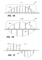
- Figure 1 is a schematic illustration of an array of N coupled emitters wherein, in the particular case shown, N = 10. An array laser with N coupled emitters has N possible coupled array modes or supermodes. A supermode is a cooperative lasing of the N optical emitters or filaments of the array laser. Since there are N emitters, there are N possible supermodes since all these emitters are optically coupled together.
- Each supermode has the property that the 1st and the Nth supermode have the same intensity pattern or envelope, the 2nd and the N-1th have the same intensity envelope, and, in general, the ith and N + 1-ith have the same intensity envelopes.
- Figure 1A shows the supermode
field amplitude pattern 10 andoverall envelope 12 for a ten emitter or element array laser wherein i = 1, i.e. the 1st or fundamental supermode. Also, illustrated in superimposed relation is the uniform and fairly rectangular shapedcharge distribution pattern 14 from current pumping of the laser. The 1st or fundamental supermode has all emitters lasing in phase with an amplitude distribution representative of half a sinusoidal cycle. This is the only supermode pattern that radiates in a single central lobe in the far field pattern because all emitters radiate in phase. - Figure 1B shows the supermode
field amplitude pattern 16 andoverall envelope 18 for the Nth supermode which, for this particular example, is i = 10. Also, illustrated in superimposed relation is the uniform and fairly rectangular shapedcharge distribution pattern 14 from current pumping of the laser. The envelope of the intensity pattern is very similar to the envelope intensity pattern shown for the 1st supermode in Figure 1A except that alternating emitters have alternating phase, i.e. are out of phase by π. As a result, this supermode will radiate in two fairly symmetrical lobes in the far field pattern. - There are eight other supermodes for i = 10. The supermode
field amplitude pattern 20 for the 2nd supermode is shown in Figure 1C wherein theenvelope 22 across the array is sinusoidal comprising one positive half cycle and one negative half cycle. The 2nd supermode will lase in two closely space symmetrical lobes in the far field pattern. - Thus, for a uniformly spaced array of identical emitters, the 1st and Nth supermode intensity envelopes are half a sinusoidal period, the 2nd and the N-1th supermode intensity envelopes are two half sinusoidal periods, etc. The phases of the individual emitters in the 1st and Nth supermodes differ. Specifically, for the 1st supermode, all emitters are in phase and for the Nth supermode, the phases alternate between zero and π. Usually the 1st and Nth supermodes have the lowest current thresholds as compared to all other supermodes because their intensity envelopes do not exhibit nulls near the center of the array where the charge density is greater as a result of current spreading and charge diffusion in the active region of the array laser. However, as previously indicated, the Nth supermode, which radiates in two lobes, has a lower current threshold of operation than the 1st supermode due to the lower gain which naturally occurs between emitting regions.
- The primary reason for supermode instability above threshold is the incomplete utilization of the injected charges with increased pumping. Specifically for a uniformly pumped array, the envelope of the individual modal field amplitudes is sinusoidal for all the supermodes and is a half cycle for the 1st and Nth supermodes as shown in Figures 1A and 1B. An estimation of the sine envelope squared intensity pattern overlap with the fairly rectangular shaped
charge distribution pattern 14 indicates that only about 50% of the injected charges will be stimulated to recombine above threshold by any single supermode. Therefore, at best, with a single supermode lasing, the differential efficiency will be reduced by that factor. More critically, the excess charges will provide excess gain, which will encourage other supermodes to lase, thereby producing a deterioration in the far field radiation pattern. For the reasons mentioned above, it is quite important to design an array laser such that at least one supermode will have an equal amplitude envelope over as much of the array as possible, such as either the 1st and Nth supermodes. - According to this invention there is provided a phased array semiconductor laser favoring emission in the 1st or Nth supermode over other potential supermodes of the laser comprises a plurality of spatially disposed laser elements formed relative to an active region to provide optical cavities for light wave generation and propagation under lasing conditions and wherein the optical field of said laser elements are coupled into the optical cavities of adjacent laser elements to provide a phase locked condition across the array. The position of the outer laser element at each end of the array are spaced closer to its adjacent laser element compared to the spacing provided between the other laser elements such that its coupling is enhanced to produce one or more supermodes with an intensity envelope which for its most part is substantially uniform and rectangular-shaped. It is preferred that the optical coupling coefficient between the outer laser elements and their adjacent laser elements is √2 K where K is the optical coupling coefficient between the other equally spaced laser elements.
- An increase in coupling coefficient between the outermost laser element waveguides at each end of an otherwise uniform array to √2 K, where K is the coupling coefficient between any other waveguides, suffices to cause the envelopes of the 1st and Nth supermodes to be equal in
waveguides 2 through N-1. This result, which is based on nearest neighbor coupling theory, when combined with gain enhancement between the waveguides relative to that within the guides themselves, should favor stable operation of the single 1st supermode. - Other objects and attainments together with a fuller understanding of the invention will become apparent and appreciated by referring to the following description and claims taken in conjunction with the accompanying drawings.
- Figure 1A illustrates the supermode field amplitude pattern and envelope for the fundamental supermode of a ten element array laser.
- Figure 1B illustrates the supermode field amplitude pattern and envelope for the Nth supermode of a ten element array laser.
- Figure 1C illustrates the supermode field amplitude pattern and envelope for the second supermode of a ten element array laser.
- Figure 2 is a schematic plan view of a multi-emitter array laser (N=10) with laser element spacing comprising this invention.
- Figure 3 illustrates the supermode field amplitude pattern and envelope for the 1st supermode(N=10) for the array laser Figure 2.
- Figure 4 illustrates the supermode pattern and envelope for the Nth supermode (N=10) for the array laser of Figure 2.
- Reference is now made to Figure 2 which illustrates the plan view of an
array laser 30 having N=10 laser elements 32-41. The general construction and structure ofarray laser 30 is well known in the art as illustrated in the aforementioned Reissue Patent 31,806 and the above mentioned article of William Streifer et al. Laser elements 33-40 oflaser 30 are mutually separated by a space, D. However, theoutside laser elements array laser 30 are more closely spaced to theiradjacent laser elements outer laser elements laser elements regions regions - As a result, the
envelopes charge distribution pattern 14 in Figure 1. The substantially uniform utilization of charge injection across most of the array will bring about stabilization of either the 1st or Nth supermode array inarray laser 30, i.e. the supermode preferred will be relatively stable with increasing current pumping above lasing threshold. - It has been determined that an increase in coupling coefficient between
outside laser elements laser elements array laser 30. The field strength of laser elements 33-40 will be about the same whereas the field strength of theoutermost laser elements envelopes - It should be noted that the field intensities of the individual laser elements will be approximately equal in all or most of the waveguides of the laser elements with the exception of the outer most waveguides of the outer most laser elements, which are at an inensity of 1/√2 compared to the remaining laser elements. Also, all or most all of the laser elements will be in phase with the exception that in some of the laser elements, the phase may be purposely reversed to shape or otherewise control the far field pattern. One example of this is the 180° phase reversal of
laser elements - Mathematical analysis also supports this result. Consider a phased array laser with N identical single mode parallel laser elements each supporting a mode E₀(y) with propagation constant β.
Laser Elements 2 through N-1 are equally spaced with centers separated by D and their interactions are characterized by a coupling coefficient K. The outermost laser elements numbered 1 and N are located in closer proximity, D, to the adjacent laser elements such that the coupling coefficient is enhanced to become √2 K. - If the individual waveguide modal amplitudes are Ul(Z), l=1,2...N and only nearest neighbor coupling is assumed, the matrix differential equation describing propagation in the array is:


The eigenfunctions and eigenvalues of Eq. (1) are the supermodes and their propagation constants, respectively. To determine these we write:

σν = β + 2K cos[π(ν-1)/(N-1)], ν = 1,2...N, (5)
which strongly resembles the result for the uniform array. The results differ in that the argument of the cosine in Eq. (5) become 0 and π, respectively, at the extreme values for the 1st supermode and the Nth supermode. These solutions do not exist for a uniform array laser.
The supermodes corresponding to the solutions of Eq. (5) are:
U(1) = col(1/√2,1,1...,1,1/√2) (7a)
and
U(N) = col(1/√2,-1,1,-1..., ±1, ∓ 1/√2). (7b)
Thus, for the 1st supermode, all but the outermost laser element modes are equal in amplitude and phase and the 1st and Nth supermodes will more effectively utilize the injected charges both at and above threshold than will the other supermodes of the array, which have unequal amplitudes across the array.
The optical intensity readiation pattern is given by:
- As a consequence of the unequal modal amplitudes of
supermodes 2 through N-1, if the 1st supermode of Eq. (7a) is favored at threshold over the Nth supermode, possibly by virtue of enhanced gain between the laser elements, or by the use of external optical elements, then that supermode will be relatively stable with increased pumping above threshold. Even if the Nth supermode has the lowest threshold, it too should remain stable with increased pumping. Moreover, because of the increased overlap between these equal intensity supermodes and the injected charge distribution, the differential efficiency will substantially exceed that of a uniform array operating in a single supermode. - To summarize, an array of identical laser elements can be designed such that the 1st and Nth supermodes have equal intensities in all but the waveguides in the outermost laser elements.
Laser elements 2 through N-1 are equally spaced and coupled;laser elements 1 and N are placed more closely to their neighboring elements such that their coupling coefficients are greater by a factor of √2. For this waveguide geometry, the 1st and Nth supermodes have uniform field strengths, except in the waveguides of theoutermost laser elements 1 and N wherein the field is weaker by 1/√2. Because these supermodes have maximum overlap with the injected charge distribution, their thresholds are lower than the other supermodes. Furthermore, above threshold, these supermodes more efficiently utilize the injected charges so that other supermodes are not encouraged to begin lasing and the single lasing mode is stable over varied current pumping range. - While the invention has been described in conjunction with a specific embodiment, it is evident to those skilled in the art that many alternatives, modifications and variations will be apparent in light of the foregoing description. Accordingly, the invention is intended to embrace all such alternatives, modifications and variations as fall within the scope of the appended claims.
Claims (4)
Applications Claiming Priority (2)
| Application Number | Priority Date | Filing Date | Title |
|---|---|---|---|
| US843485 | 1986-03-24 | ||
| US06/843,485 US4719630A (en) | 1986-03-24 | 1986-03-24 | Phased array semiconductor lasers with uniform and stable supermode |
Publications (3)
| Publication Number | Publication Date |
|---|---|
| EP0239352A2 true EP0239352A2 (en) | 1987-09-30 |
| EP0239352A3 EP0239352A3 (en) | 1988-09-28 |
| EP0239352B1 EP0239352B1 (en) | 1991-10-02 |
Family
ID=25290127
Family Applications (1)
| Application Number | Title | Priority Date | Filing Date |
|---|---|---|---|
| EP87302498A Expired EP0239352B1 (en) | 1986-03-24 | 1987-03-24 | Phased array semiconductor lasers |
Country Status (4)
| Country | Link |
|---|---|
| US (1) | US4719630A (en) |
| EP (1) | EP0239352B1 (en) |
| JP (1) | JPH0750812B2 (en) |
| DE (1) | DE3773419D1 (en) |
Cited By (2)
| Publication number | Priority date | Publication date | Assignee | Title |
|---|---|---|---|---|
| US5568498A (en) * | 1993-09-10 | 1996-10-22 | Telefonaktiebolaget Lm Ericsson | Laser device with laser structures connected in series in an optical cavity |
| US5781575A (en) * | 1993-09-10 | 1998-07-14 | Telefonaktiebolaget Lm Ericsson | Surface emitting laser device with a vertical cavity |
Families Citing this family (5)
| Publication number | Priority date | Publication date | Assignee | Title |
|---|---|---|---|---|
| JPS63306689A (en) * | 1987-05-22 | 1988-12-14 | シーメンス、アクチエンゲゼルシヤフト | Laterlly coupled laser diode array |
| US4797894A (en) * | 1987-08-21 | 1989-01-10 | Xerox Corporation | Alignment method and arrangement for external optical feedback for semiconductor diode lasers |
| JPH084187B2 (en) * | 1988-02-01 | 1996-01-17 | 三菱電機株式会社 | Semiconductor laser |
| GB2384617B (en) * | 2001-10-15 | 2005-06-22 | Arima Optoelectronic | Semiconductor laser diodes |
| US7532392B1 (en) | 2006-03-29 | 2009-05-12 | Hrl Laboratories | Dark channel array |
Family Cites Families (4)
| Publication number | Priority date | Publication date | Assignee | Title |
|---|---|---|---|---|
| US31806A (en) * | 1861-03-26 | Chukjsr | ||
| USRE31806E (en) | 1978-10-30 | 1985-01-15 | Xerox Corporation | Monolithic multi-emitting laser device |
| US4594719A (en) * | 1984-01-19 | 1986-06-10 | Rca Corporation | Phase-locked laser array having a non-uniform spacing between lasing regions |
| US4624000A (en) * | 1984-11-01 | 1986-11-18 | Xerox Corporation | Phased array semiconductor lasers with preferred emission in a single lobe |
-
1986
- 1986-03-24 US US06/843,485 patent/US4719630A/en not_active Expired - Fee Related
-
1987
- 1987-03-17 JP JP62062335A patent/JPH0750812B2/en not_active Expired - Lifetime
- 1987-03-24 EP EP87302498A patent/EP0239352B1/en not_active Expired
- 1987-03-24 DE DE8787302498T patent/DE3773419D1/en not_active Expired - Fee Related
Non-Patent Citations (3)
| Title |
|---|
| ELECTRONICS LETTERS, vol. 20, no. 17, 16th August 1984, pages 695-697, Staines, Middlesex, GB; D.E. ACKLEY: "Phase-locked injection laser arrays with nonuniform stripe spacing" * |
| LASER FOCUS, vol. 20, no. 6, June 1984, pages 100-102,105-106,108-110, Newton, Massachusetts, US; W. STREIFER et al.: "Phased array diode lasers" * |
| OPTICS LETTERS, vol. 10, no. 4, April 1984, pages 125-127, Optical Society of America, New York, US; E. KAPON et al.: "Supermode analysis of phase-locked arrays of semiconductor lasers" * |
Cited By (2)
| Publication number | Priority date | Publication date | Assignee | Title |
|---|---|---|---|---|
| US5568498A (en) * | 1993-09-10 | 1996-10-22 | Telefonaktiebolaget Lm Ericsson | Laser device with laser structures connected in series in an optical cavity |
| US5781575A (en) * | 1993-09-10 | 1998-07-14 | Telefonaktiebolaget Lm Ericsson | Surface emitting laser device with a vertical cavity |
Also Published As
| Publication number | Publication date |
|---|---|
| EP0239352A3 (en) | 1988-09-28 |
| JPH0750812B2 (en) | 1995-05-31 |
| US4719630A (en) | 1988-01-12 |
| EP0239352B1 (en) | 1991-10-02 |
| JPS62230080A (en) | 1987-10-08 |
| DE3773419D1 (en) | 1991-11-07 |
Similar Documents
| Publication | Publication Date | Title |
|---|---|---|
| EP0363076B1 (en) | Semiconductor laser array having high power and high beam quality | |
| US7978745B2 (en) | Two-dimensional photonic crystal surface-emitting laser | |
| KR0131920B1 (en) | Circular Grating Surface Emission Laser Diode Array | |
| US4694459A (en) | Hybrid gain/index guided semiconductor lasers and array lasers | |
| KR20010079633A (en) | Injection laser | |
| US4751711A (en) | Asymmetric offset stripe laser for emission in a single lobe | |
| US4947401A (en) | Semiconductor laser array | |
| CN101841129A (en) | Monolithic phase-locked surface-emitting distributed feedback semiconductor laser array | |
| JPH0318086A (en) | Emitted-light coupling system of semiconductor radiation element and emitted-light processing array using said system | |
| US4624000A (en) | Phased array semiconductor lasers with preferred emission in a single lobe | |
| EP0239352B1 (en) | Phased array semiconductor lasers | |
| US5159604A (en) | Antiguided semiconductor laser array with edge reflectors | |
| Botez et al. | Phase-locked laser arrays revisited | |
| US4852113A (en) | Laser array with wide-waveguide coupling region | |
| Streifer et al. | Phased‐array lasers with a uniform, stable supermode | |
| EP1012933B1 (en) | Laser device | |
| KR940011107B1 (en) | Semiconductor laser device | |
| Streifer et al. | Analysis of a Y‐junction semiconductor laser array | |
| Botez et al. | Diffraction‐limited‐beam, high‐power operation from X‐junction coupled phase‐locked arrays of AlGaAs/GaAs diode lasers | |
| US4868839A (en) | Semiconductor laser array with nonplanar diffraction region | |
| US4866724A (en) | Wide-waveguide interferometric array with interelement losses | |
| US5050180A (en) | Phase-locked arrays of coupled X-junctions | |
| CN114640020B (en) | Supersymmetric semiconductor lasers and their applications | |
| US4771433A (en) | Semiconductor laser device | |
| Figueroa et al. | Modeling of the optical characteristics for twin-channel laser (TCL) structures |
Legal Events
| Date | Code | Title | Description |
|---|---|---|---|
| PUAI | Public reference made under article 153(3) epc to a published international application that has entered the european phase |
Free format text: ORIGINAL CODE: 0009012 |
|
| AK | Designated contracting states |
Kind code of ref document: A2 Designated state(s): DE FR GB IT |
|
| PUAL | Search report despatched |
Free format text: ORIGINAL CODE: 0009013 |
|
| AK | Designated contracting states |
Kind code of ref document: A3 Designated state(s): DE FR GB IT |
|
| 17P | Request for examination filed |
Effective date: 19890313 |
|
| 17Q | First examination report despatched |
Effective date: 19901203 |
|
| GRAA | (expected) grant |
Free format text: ORIGINAL CODE: 0009210 |
|
| AK | Designated contracting states |
Kind code of ref document: B1 Designated state(s): DE FR GB IT |
|
| REF | Corresponds to: |
Ref document number: 3773419 Country of ref document: DE Date of ref document: 19911107 |
|
| ET | Fr: translation filed | ||
| ITF | It: translation for a ep patent filed | ||
| PLBE | No opposition filed within time limit |
Free format text: ORIGINAL CODE: 0009261 |
|
| STAA | Information on the status of an ep patent application or granted ep patent |
Free format text: STATUS: NO OPPOSITION FILED WITHIN TIME LIMIT |
|
| 26N | No opposition filed | ||
| PGFP | Annual fee paid to national office [announced via postgrant information from national office to epo] |
Ref country code: FR Payment date: 19950309 Year of fee payment: 9 |
|
| PGFP | Annual fee paid to national office [announced via postgrant information from national office to epo] |
Ref country code: GB Payment date: 19950315 Year of fee payment: 9 |
|
| PGFP | Annual fee paid to national office [announced via postgrant information from national office to epo] |
Ref country code: DE Payment date: 19950322 Year of fee payment: 9 |
|
| PG25 | Lapsed in a contracting state [announced via postgrant information from national office to epo] |
Ref country code: GB Effective date: 19960324 |
|
| GBPC | Gb: european patent ceased through non-payment of renewal fee |
Effective date: 19960324 |
|
| PG25 | Lapsed in a contracting state [announced via postgrant information from national office to epo] |
Ref country code: FR Effective date: 19961129 |
|
| PG25 | Lapsed in a contracting state [announced via postgrant information from national office to epo] |
Ref country code: DE Effective date: 19961203 |
|
| REG | Reference to a national code |
Ref country code: FR Ref legal event code: ST |
|
| PG25 | Lapsed in a contracting state [announced via postgrant information from national office to epo] |
Ref country code: IT Free format text: LAPSE BECAUSE OF NON-PAYMENT OF DUE FEES Effective date: 20050324 |