EP0237331A2 - Reduced crosstalk optical switch - Google Patents
Reduced crosstalk optical switch Download PDFInfo
- Publication number
- EP0237331A2 EP0237331A2 EP87302064A EP87302064A EP0237331A2 EP 0237331 A2 EP0237331 A2 EP 0237331A2 EP 87302064 A EP87302064 A EP 87302064A EP 87302064 A EP87302064 A EP 87302064A EP 0237331 A2 EP0237331 A2 EP 0237331A2
- Authority
- EP
- European Patent Office
- Prior art keywords
- refractive index
- optical switch
- liquid crystal
- prisms
- chosen
- Prior art date
- Legal status (The legal status is an assumption and is not a legal conclusion. Google has not performed a legal analysis and makes no representation as to the accuracy of the status listed.)
- Withdrawn
Links
Images
Classifications
-
- G—PHYSICS
- G02—OPTICS
- G02F—OPTICAL DEVICES OR ARRANGEMENTS FOR THE CONTROL OF LIGHT BY MODIFICATION OF THE OPTICAL PROPERTIES OF THE MEDIA OF THE ELEMENTS INVOLVED THEREIN; NON-LINEAR OPTICS; FREQUENCY-CHANGING OF LIGHT; OPTICAL LOGIC ELEMENTS; OPTICAL ANALOGUE/DIGITAL CONVERTERS
- G02F1/00—Devices or arrangements for the control of the intensity, colour, phase, polarisation or direction of light arriving from an independent light source, e.g. switching, gating or modulating; Non-linear optics
- G02F1/29—Devices or arrangements for the control of the intensity, colour, phase, polarisation or direction of light arriving from an independent light source, e.g. switching, gating or modulating; Non-linear optics for the control of the position or the direction of light beams, i.e. deflection
- G02F1/31—Digital deflection, i.e. optical switching
- G02F1/315—Digital deflection, i.e. optical switching based on the use of controlled internal reflection
Definitions
- the present invention concerns optical switches utilising a liquid crystal interface. Such switches are well known.
- the present invention has for one object to provide an optical switch with a low crosstalk factor.
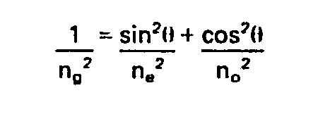
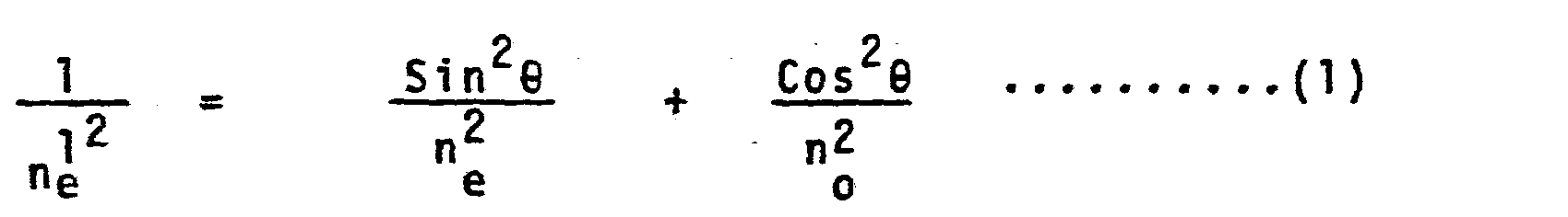
- the present invention consists in an optical switch comprising two glass prisms located on either side of a liquid crystal interface, wherein the liquid crystal is chosen to have a positive dielectric anisotropy with an extraordinary refractive index n e and an ordinary refractive index n o , and wherein the refractive index of the glass prisms, n g is chosen so that and wherein ⁇ is the base angle of the prisms.
- each prism may carry a transparent electrode which is approximately 100 - 150 A thick and each electrode may be covered with a polymer having the same refractive index as the glass prisms.
- an optical switching array incorporating a plurality of optical switches as set out hereinbefore, and including means for applying a switching voltage in the order of 100 volts to the electrodes of each of the switches.
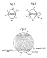
- Figure 1 shows the basic design of an optical switch.
- This comprises two glass prisms 10,11 in the shape of prism trapeziums whose faces are polished to minor flatness.
- One face of each prism is coated with a thin layer of a transparent conducting material such as Indium Tin Oxide which acts as an electrode.
- This layer is covered by another thin layer of a polymer.
- the polymer layer in known optical switches-of this type, is mechanically rubbed in the X direction using a cloth. The rubbing operation introduces microscopic scratches in the polymer whose purpose will be explained later.
- the two prisms 10, 11 are placed together with the double coated faces facing each other and are held spaced apart by a seal 12 which is about 9 microns thick.
- the cavity between the faces is filled with a liquid crystal.
- Such a switch is capable of switching a ray of light incident at A to either B or C.
- the input ray of light is linearly polarised in the x,2 plane and may originate from an optical fibre attached to the side of the prism 10 by means of a focussing lens, or from a gas laser. In any case the incident ray of light A always strikes the face of the prism 10 normally.
- the molecules of the liquid crystal passes positive dielectric anisotropy.
- the refractive index, n of the glass prisms 10, 11 is chosen to be very close to the extraordinary index, net of the liquid crystal.
- the incoming ray of light A "sees" the higher refractive index, n , of the crystal which is very close to that, n e , of the glass, and in the absence of any optical discontinuity passes out of the switch in direction B.
- the liquid crystal molecules align parallel to the adjacent parallel surfaces of the glass prisms 10,11 with their long axes parallel to the microscopic grooves in the polymer layer.
- the ray of light A now sees the lower of the two liquid crystal refractive indices, n , and if ⁇ , the base angle of prism 10 is chosen that Sing n /n , then the light ray undergoes total internal reflection and passes out along C.
- the present invention is concerned with reducing crosstalk to a minimum and it has been discovered that the use of positive dielectric liquid crystals in the presently described embodiment is a factor in reducing crosstalk as they have greater optical anisotropy than negative crystals. They are also more tightly bound at the cell boundaries.
- the refractive index of prisms 10, 11 is selected to satisfy this equation.
- the polymer layer is chosen so that it has a refractive index similar to that of the glass prisms 10, 11.
- the chosen material is polyvinyl carazole.
- the thickness of this layer is defined such that it is substantially the same as the minimum depth of groove required to align the liquid crystal molecules in the OFF state.
- the thickness of the elctrode layer is chosen, in the present embodiment, to be between 100 and 150 Furthermore it has been discovered that when known optical switches are in the ON state there is a region of unswitched liquid crystal very close to the surfaces of the cell which finds a lower potential state by aligning with the microscopic grooves rather than with the applied electric field. In order to reduce effect the liquid crystal layer in the present embodiment is arranged to be switched at 100 volts, substantially in excess of the normal 12 volts. A range of 50 to 125 volts cam be used with higher voltages giving still further improvement.
- the glass for the prisms had a refractive index (n g ) 1.693.
- optical switch which has just been described has in operation extremely low crosstalk and can thus be used in multi-switch structures to handle a plurality of input signals and to switch them between a plurality of outputs.
Abstract
Description
- The present invention concerns optical switches utilising a liquid crystal interface. Such switches are well known.
- However a major problem which has hindered the wider use of liquid crystal switches is the problem of crosstalk, and the present invention has for one object to provide an optical switch with a low crosstalk factor.
- Accordingly from one aspect the present invention consists in an optical switch comprising two glass prisms located on either side of a liquid crystal interface, wherein the liquid crystal is chosen to have a positive dielectric anisotropy with an extraordinary refractive index ne and an ordinary refractive index no, and wherein the refractive index of the glass prisms, ng is chosen so that

- According to a feature of the invention, each prism may carry a transparent electrode which is approximately 100 - 150 A thick and each electrode may be covered with a polymer having the same refractive index as the glass prisms.
- In accordance with a second aspect of the invention there is provided an optical switching array incorporating a plurality of optical switches as set out hereinbefore, and including means for applying a switching voltage in the order of 100 volts to the electrodes of each of the switches.
- In order that the present invention may be more readily understood, an embodiment thereof will now be described by way of example and with reference to the accompanying drawings, in which:
- Figure 1 shows an optical switch incorporating a liquid crystal interface in the OFF condition,
- Figure 2 shows the same switch in the ON condition, and
- Figure 3 is an enlargement of part of Figure 2.
- Referring now to the drawings Figure 1 shows the basic design of an optical switch. This comprises two
glass prisms - The two
prisms seal 12 which is about 9 microns thick. The cavity between the faces is filled with a liquid crystal. - Such a switch is capable of switching a ray of light incident at A to either B or C.
- The input ray of light is linearly polarised in the x,2 plane and may originate from an optical fibre attached to the side of the
prism 10 by means of a focussing lens, or from a gas laser. In any case the incident ray of light A always strikes the face of theprism 10 normally. - In the present embodiment the molecules of the liquid crystal passes positive dielectric anisotropy. Furthermore the refractive index, n , of the
glass prisms - When the electrical potential is removed the liquid crystal molecules align parallel to the adjacent parallel surfaces of the
glass prisms prism 10 is chosen that Sing n /n , then the light ray undergoes total internal reflection and passes out along C. - Previously all known liquid crystal switches have suffered from a major "crosstalk" problem when in the "ON" state. The crosstalk is caused by spurious reflections in the region of the liquid crystal interface. These reflections are due to the false assumption that the light sees no optical discontinuation when passing through the switch in its "ON" state.
- As previously mentioned the present invention is concerned with reducing crosstalk to a minimum and it has been discovered that the use of positive dielectric liquid crystals in the presently described embodiment is a factor in reducing crosstalk as they have greater optical anisotropy than negative crystals. They are also more tightly bound at the cell boundaries.
- In the present embodiment the possibility of optical discontinuities in the ON state is also reduced by appreciating that the incident light in the ON state does not actually see n the extraordinary refractive index of the liquid crystal but a slightly lower index n given by the equation:
- Thus in the present embodiment the refractive index of
prisms glass prisms - The thickness of the elctrode layer is chosen, in the present embodiment, to be between 100 and 150 Furthermore it has been discovered that when known optical switches are in the ON state there is a region of unswitched liquid crystal very close to the surfaces of the cell which finds a lower potential state by aligning with the microscopic grooves rather than with the applied electric field. In order to reduce effect the liquid crystal layer in the present embodiment is arranged to be switched at 100 volts, substantially in excess of the normal 12 volts. A range of 50 to 125 volts cam be used with higher voltages giving still further improvement.
- In the embodiment of the switch being described, the glass for the prisms had a refractive index (ng) 1.693. The liquid crystal was KIS (BDH) for which ne = 1.73 and no = 1.53. From the equation 1 the angle 6 at which the refractive indices are matched is 67.
- The optical switch which has just been described has in operation extremely low crosstalk and can thus be used in multi-switch structures to handle a plurality of input signals and to switch them between a plurality of outputs.
Claims (4)

Applications Claiming Priority (2)
| Application Number | Priority Date | Filing Date | Title |
|---|---|---|---|
| GB8606153 | 1986-03-12 | ||
| GB868606153A GB8606153D0 (en) | 1986-03-12 | 1986-03-12 | Optical switch |
Publications (2)
| Publication Number | Publication Date |
|---|---|
| EP0237331A2 true EP0237331A2 (en) | 1987-09-16 |
| EP0237331A3 EP0237331A3 (en) | 1989-07-12 |
Family
ID=10594492
Family Applications (1)
| Application Number | Title | Priority Date | Filing Date |
|---|---|---|---|
| EP87302064A Withdrawn EP0237331A3 (en) | 1986-03-12 | 1987-03-11 | Reduced crosstalk optical switch |
Country Status (2)
| Country | Link |
|---|---|
| EP (1) | EP0237331A3 (en) |
| GB (2) | GB8606153D0 (en) |
Families Citing this family (1)
| Publication number | Priority date | Publication date | Assignee | Title |
|---|---|---|---|---|
| GB8626966D0 (en) * | 1986-11-12 | 1986-12-10 | Gen Electric Co Plc | Optical switch |
Citations (2)
| Publication number | Priority date | Publication date | Assignee | Title |
|---|---|---|---|---|
| EP0015139A1 (en) * | 1979-02-21 | 1980-09-03 | Sperry Corporation | Electro-optical switching matrix |
| US4516837A (en) * | 1983-02-22 | 1985-05-14 | Sperry Corporation | Electro-optical switch for unpolarized optical signals |
-
1986
- 1986-03-12 GB GB868606153A patent/GB8606153D0/en active Pending
-
1987
- 1987-03-11 EP EP87302064A patent/EP0237331A3/en not_active Withdrawn
- 1987-03-11 GB GB8705705A patent/GB2187860B/en not_active Expired
Patent Citations (2)
| Publication number | Priority date | Publication date | Assignee | Title |
|---|---|---|---|---|
| EP0015139A1 (en) * | 1979-02-21 | 1980-09-03 | Sperry Corporation | Electro-optical switching matrix |
| US4516837A (en) * | 1983-02-22 | 1985-05-14 | Sperry Corporation | Electro-optical switch for unpolarized optical signals |
Non-Patent Citations (2)
| Title |
|---|
| APPLIED OPTICS, vol. 12, no. 10, October 1973, pages 2309-2311; R.A. KASHNOW et al.: "Total-reflection liquid-crystal electrooptic device" * |
| APPLIED OPTICS, vol. 13, no. 8, August 1974, pages 1802-1806; G. LABRUNIE et al.: "Nematic liquid crystal digital light deflector" * |
Also Published As
| Publication number | Publication date |
|---|---|
| GB2187860B (en) | 1989-11-15 |
| GB8705705D0 (en) | 1987-04-15 |
| GB8606153D0 (en) | 1986-04-16 |
| EP0237331A3 (en) | 1989-07-12 |
| GB2187860A (en) | 1987-09-16 |
Similar Documents
| Publication | Publication Date | Title |
|---|---|---|
| US5276747A (en) | Polarization-independent optical switch/attenuator | |
| US4789228A (en) | Electrically controlled optical switching device | |
| EP0029737B1 (en) | Electro-optical switching devices | |
| US4828362A (en) | Optical switch | |
| US6297899B1 (en) | Discrete element light modulating microstructure devices | |
| US4720172A (en) | Liquid crystal optical switching device | |
| US4720171A (en) | Liquid crystal optical switching device having reduced crosstalk | |
| EP0100178B1 (en) | Polarizing elements | |
| US5317429A (en) | Trilayer nematic liquid crystal optical switching device | |
| KR20020010685A (en) | Electrophoretic, high index and phase transition control of total internal reflection in high efficiency variable reflectivity image displays | |
| US4815827A (en) | Optical switch structures | |
| EP0229287B1 (en) | Optical change-over switch | |
| EP0023741A1 (en) | Electrophoretic image display device | |
| US4737019A (en) | Liquid crystal optical switching device having minimized internal light path | |
| EP0015139B1 (en) | Electro-optical switching matrix | |
| EP0237331A2 (en) | Reduced crosstalk optical switch | |
| US6486996B1 (en) | Discrete element light modulating microstructure devices | |
| Skinner et al. | A low crosstalk microoptic liquid crystal switch | |
| US7046425B1 (en) | Multi-stage optical switching device | |
| GB2198255A (en) | Optical switch | |
| US4669831A (en) | Total internal reflection modulator/deflector | |
| JPS62153837A (en) | Optical path switch | |
| US7142268B1 (en) | Enhanced light-scattering display | |
| US3506335A (en) | Light deflecting device | |
| KR100724743B1 (en) | Transparent Type Display Device Using Micro Electro-mechanical System |
Legal Events
| Date | Code | Title | Description |
|---|---|---|---|
| PUAI | Public reference made under article 153(3) epc to a published international application that has entered the european phase |
Free format text: ORIGINAL CODE: 0009012 |
|
| AK | Designated contracting states |
Kind code of ref document: A2 Designated state(s): DE FR |
|
| 17P | Request for examination filed |
Effective date: 19880308 |
|
| PUAL | Search report despatched |
Free format text: ORIGINAL CODE: 0009013 |
|
| AK | Designated contracting states |
Kind code of ref document: A3 Designated state(s): DE FR |
|
| STAA | Information on the status of an ep patent application or granted ep patent |
Free format text: STATUS: THE APPLICATION IS DEEMED TO BE WITHDRAWN |
|
| 18D | Application deemed to be withdrawn |
Effective date: 19900113 |
|
| RIN1 | Information on inventor provided before grant (corrected) |
Inventor name: SKINNER, JEFFREY DAVID |