EP0235734B1 - Reduction-reoxidation type semiconductor ceramic capacitor and method of manufacturing thereof - Google Patents
Reduction-reoxidation type semiconductor ceramic capacitor and method of manufacturing thereof Download PDFInfo
- Publication number
- EP0235734B1 EP0235734B1 EP87102649A EP87102649A EP0235734B1 EP 0235734 B1 EP0235734 B1 EP 0235734B1 EP 87102649 A EP87102649 A EP 87102649A EP 87102649 A EP87102649 A EP 87102649A EP 0235734 B1 EP0235734 B1 EP 0235734B1
- Authority
- EP
- European Patent Office
- Prior art keywords
- semiconductor ceramic
- electrode
- reoxidated
- dielectric layer
- reduction
- Prior art date
- Legal status (The legal status is an assumption and is not a legal conclusion. Google has not performed a legal analysis and makes no representation as to the accuracy of the status listed.)
- Expired - Lifetime
Links
- 239000004065 semiconductor Substances 0.000 title claims description 74
- 238000010405 reoxidation reaction Methods 0.000 title claims description 34
- 239000003985 ceramic capacitor Substances 0.000 title claims description 26
- 238000004519 manufacturing process Methods 0.000 title claims description 8
- 239000000919 ceramic Substances 0.000 claims description 49
- 239000007772 electrode material Substances 0.000 claims description 14
- 229910052751 metal Inorganic materials 0.000 claims description 14
- 239000002184 metal Substances 0.000 claims description 14
- 238000010438 heat treatment Methods 0.000 claims description 13
- 150000002739 metals Chemical class 0.000 claims description 10
- 229910052782 aluminium Inorganic materials 0.000 claims description 6
- 229910052759 nickel Inorganic materials 0.000 claims description 6
- 229910052718 tin Inorganic materials 0.000 claims description 6
- 229910052725 zinc Inorganic materials 0.000 claims description 6
- 150000001875 compounds Chemical class 0.000 claims description 4
- 238000009877 rendering Methods 0.000 claims description 4
- 239000004020 conductor Substances 0.000 claims description 2
- 239000003990 capacitor Substances 0.000 description 19
- 230000000694 effects Effects 0.000 description 8
- 239000000843 powder Substances 0.000 description 7
- 239000002003 electrode paste Substances 0.000 description 6
- 230000004888 barrier function Effects 0.000 description 5
- 239000011521 glass Substances 0.000 description 4
- 239000000463 material Substances 0.000 description 4
- 238000005498 polishing Methods 0.000 description 4
- 230000009471 action Effects 0.000 description 3
- 230000015556 catabolic process Effects 0.000 description 3
- 238000000034 method Methods 0.000 description 3
- 229910020617 PbO—B2O3—SiO2 Inorganic materials 0.000 description 2
- GWEVSGVZZGPLCZ-UHFFFAOYSA-N Titan oxide Chemical compound O=[Ti]=O GWEVSGVZZGPLCZ-UHFFFAOYSA-N 0.000 description 2
- 239000011230 binding agent Substances 0.000 description 2
- 150000002736 metal compounds Chemical class 0.000 description 2
- 239000000203 mixture Substances 0.000 description 2
- 235000011837 pasties Nutrition 0.000 description 2
- 230000001603 reducing effect Effects 0.000 description 2
- 230000009467 reduction Effects 0.000 description 2
- 239000004372 Polyvinyl alcohol Substances 0.000 description 1
- QVGXLLKOCUKJST-UHFFFAOYSA-N atomic oxygen Chemical compound [O] QVGXLLKOCUKJST-UHFFFAOYSA-N 0.000 description 1
- 230000015572 biosynthetic process Effects 0.000 description 1
- 230000008021 deposition Effects 0.000 description 1
- 238000009792 diffusion process Methods 0.000 description 1
- 238000007772 electroless plating Methods 0.000 description 1
- 239000007789 gas Substances 0.000 description 1
- 238000005470 impregnation Methods 0.000 description 1
- 238000009413 insulation Methods 0.000 description 1
- 238000005259 measurement Methods 0.000 description 1
- 238000012986 modification Methods 0.000 description 1
- 230000004048 modification Effects 0.000 description 1
- 239000001301 oxygen Substances 0.000 description 1
- 229910052760 oxygen Inorganic materials 0.000 description 1
- 239000002245 particle Substances 0.000 description 1
- 230000002093 peripheral effect Effects 0.000 description 1
- 229920002451 polyvinyl alcohol Polymers 0.000 description 1
- 230000008569 process Effects 0.000 description 1
- 239000000126 substance Substances 0.000 description 1
- 239000012808 vapor phase Substances 0.000 description 1
Images
Classifications
-
- H—ELECTRICITY
- H01—ELECTRIC ELEMENTS
- H01G—CAPACITORS; CAPACITORS, RECTIFIERS, DETECTORS, SWITCHING DEVICES, LIGHT-SENSITIVE OR TEMPERATURE-SENSITIVE DEVICES OF THE ELECTROLYTIC TYPE
- H01G4/00—Fixed capacitors; Processes of their manufacture
- H01G4/002—Details
- H01G4/018—Dielectrics
- H01G4/06—Solid dielectrics
- H01G4/08—Inorganic dielectrics
- H01G4/12—Ceramic dielectrics
-
- H—ELECTRICITY
- H01—ELECTRIC ELEMENTS
- H01G—CAPACITORS; CAPACITORS, RECTIFIERS, DETECTORS, SWITCHING DEVICES, LIGHT-SENSITIVE OR TEMPERATURE-SENSITIVE DEVICES OF THE ELECTROLYTIC TYPE
- H01G4/00—Fixed capacitors; Processes of their manufacture
- H01G4/002—Details
- H01G4/018—Dielectrics
- H01G4/06—Solid dielectrics
- H01G4/08—Inorganic dielectrics
- H01G4/12—Ceramic dielectrics
- H01G4/1272—Semiconductive ceramic capacitors
-
- A—HUMAN NECESSITIES
- A61—MEDICAL OR VETERINARY SCIENCE; HYGIENE
- A61B—DIAGNOSIS; SURGERY; IDENTIFICATION
- A61B18/00—Surgical instruments, devices or methods for transferring non-mechanical forms of energy to or from the body
- A61B18/18—Surgical instruments, devices or methods for transferring non-mechanical forms of energy to or from the body by applying electromagnetic radiation, e.g. microwaves
- A61B18/20—Surgical instruments, devices or methods for transferring non-mechanical forms of energy to or from the body by applying electromagnetic radiation, e.g. microwaves using laser
- A61B2018/2035—Beam shaping or redirecting; Optical components therefor
- A61B2018/20351—Scanning mechanisms
- A61B2018/20353—Scanning in three dimensions [3D]
-
- Y—GENERAL TAGGING OF NEW TECHNOLOGICAL DEVELOPMENTS; GENERAL TAGGING OF CROSS-SECTIONAL TECHNOLOGIES SPANNING OVER SEVERAL SECTIONS OF THE IPC; TECHNICAL SUBJECTS COVERED BY FORMER USPC CROSS-REFERENCE ART COLLECTIONS [XRACs] AND DIGESTS
- Y10—TECHNICAL SUBJECTS COVERED BY FORMER USPC
- Y10T—TECHNICAL SUBJECTS COVERED BY FORMER US CLASSIFICATION
- Y10T29/00—Metal working
- Y10T29/43—Electric condenser making
- Y10T29/435—Solid dielectric type
Definitions
- the present invention relates to a ceramic capacitor and manufacturing thereof, which profitably employs as a dielectric substance a reoxidated layer formed on the surface of reduced semiconductor ceramic by reoxidating the reduced semiconductor ceramic.
- Prior reduction-reoxidation type semiconductor ceramic capacitors are substantially classified into two types.
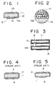
- One is, as illustrated in Fig. 4, adapted to heat-treat semiconductor ceramic 1 to thereby form a reoxidated dielectric layer on the surface of the semiconductor ceramic 1 as a dielectric layer 2, and thereafter dispose a pair of electrodes 3, 4 on the dielectric layer 2 in confronting relation.
- the other is adapted to employ as an electrode material electrode paste containing glass frit without rendering a semiconductor ceramic to a reoxidation treatment, and to diffuse in vapor phase, upon baking the electrode paste, a glass frit component contained in the electrode paste onto the surface of the semiconductor ceramic for forming a barrier layer as a dielectric layer on the surface of the semiconductor surface.
- Such a reduction-reoxidation type semiconductor ceramic capacitor which assured an extremely thin dielectric layer 2, was developed as a capacitor providing large electrostatic capacity.
- the structure shown in Fig. 4 permits the semiconductor layer 1 to be located between the electrodes 3, 4 on both sides thereof and functions as another electrode holding the dielectric layer 2 therebetween. Accordingly, the structure appears as if there exist two capacitors connected in series to each other, and hence is limited in its electrostatic capacity.
- capacitors are considered: one is, as illustrated in Fig. 5, adapted to previously heat-treat a semiconductor ceramic 1 to form on the surface thereof a reoxidation layer as part of a dielectric layer 2, and remove part of the dielectric layer 2 by polishing, and furthermore to place electrodes 3, 4 respectively on the remaining dielectric layer 2 and on the semiconductor ceramic 1 exposed by the above polishing; the other is adapted to employ, upon baking the electrode 4 when forming the same, electrode paste containing metal or a metal compound serving to prevent a barrier layer from being formed on the surface of the semiconductor ceramic 1, and to render the electrode paste to baking together with the other electrode 3.
- the former suffered from problems of, upon increasing the productivity, the increased number of fabrication processes accompanying fine polishing of the semiconductor ceramic 1 as well as increased troubles attendant on the damaged semiconductor ceramic 1.
- a barrier layer can be formed on the surface of the semiconductor ceramic 1 at the temperature of baking of the electrodes 3, 4, but it is difficult in fact to provide a sufficiently thick dielectric layer 2. For this reason there appears such a rectification effect by the action of the barrier layer that the amount of a current flowing therethrough is extremely different depending on the polarities of voltage applied between the electrodes 3, 4.
- a ceramic capacitor according to a first aspect of the invention comprising a semiconductor ceramic 11, a reoxidated dielectric layer 12 formed on the whole surface of said semiconductor ceramic; and at least a pair of electrodes 13, 14 formed on said reoxidated dielectric layer, on at least two opposite surfaces of said semiconductor ceramic is characterized in that one 14 of said electrodes is formed with an electrical conductor containing one kind or more of metals or compounds thereof selected from Zn, Al, Ni, and Sn; and one kind or more of said metals is diffused in extremely small quantities into the interior of a portion of said reoxidated dielectric layer, said portion making contact with said one electrode.
- a method of manufacturing said ceramic capacitor comprises the steps of rendering a semiconductor ceramic to a heat treatment at a temperature in the range of 950 to 1200°C to thereby form a reoxidated dielectric layer on the whole surface of said semiconductor ceramic; providing an electrode material layer containing one kind or more of metals or metal compounds selected from Zn, Al, Ni, and Sn on a portion of the semiconductor ceramic for forming one of at least a pair of electrodes; and baking said electrode material layer so provided at a temperature in the range of 600 to 850°C to thereby form said one electrode 14 and diffuse one kind or more of said metals in extremely small quantities into the interior of a portion of said reoxidated dielectric layer, said portion making contact with said one electrode.
- the semiconductor ceramic 11 are rendered to a heat treatment at temperature of from 950 to 1200 °C to thereby reoxidate the whole surface of the semiconductor ceramic for forming the reoxidated dielectric layer 12 having its thickness of about 10 ⁇ .
- the resulting reduction-reoxidation type ceramic capacitor is adapted to permit the semiconductor ceramic 11 and the electrode 14 to be connected with each other in an electrically conductive manner without interposition of the reoxidated dielectric layer 12. Therefore, the electrodes 13 and 14 are substantially adapted to face each other while holding one layer of the reoxidated dielectric layer 12 therebetween in a sandwiching relation to assure large electrostatic capacitance.
- the temperature of a heat treatment upon rendering the semiconductor ceramic 11 to a reoxidation treatment was limited within the range of from 950 to 1200 °C, the reason of which is as follows: provided the temperature lies below the above temperature range, the surface of the semiconductor ceramic 11 is reoxidated insufficiently to provide satisfactory insulating characteristics. Contrariwise, with the heat treatment temperature exceeding this temperature range, the reoxidation of the semiconductor ceramic 11 is extremely speeded up to result in the thickness of the reoxidated dielectric layer 12 located on the surface of the semiconductor ceramic 11 being increased in excess, and thus large electrostatic capacity is unlikely to be obtained.
- the heat treatment temperature upon baking the electrodes 13, 14 was limited within the range of from 600 to 850°C, the reason of which is as follows: provided the heat treatment temperature lies below this range, reduction on the side of the electrode 14 and diffusion of the metal components into the reoxidated semiconductor layer 12 are difficult to be effected, and hence large electrostatic capacity is unlikely to be obtained.
- the heat treatment temperature exceeding this temperature range the electrode 14 is reoxidated to result in an undesirable increase of electric resistance with the possibility of a function thereof as an electrode being not obtainable.
- material powders were measured to provide 100 mol of BaTio3, 3 mol of Na2O3, 6 mol of TiO2, and 0.5 mol of MnO, and wet blended for 15 hours in a ball mill. These material powders were calcinated for 2 hours at 1150 °C, and again wet blended for 15 hours in a ball mill.
- the material powders so treated were granulated by addition of polyvinyl alcohol, and molded into disks with 8.4 mm diameter and 0.5 mm thickness.
- the resulting molded materials were heat-treated for 3 hours at 1350 °C in the atmosphere and furthermore for 2 hours at 1150 °C in the reducing atmosphere of N2-H2 gas to yield a semiconductor ceramic 11.
- the resulting semiconductor ceramic 11 were heat-treated in the atmosphere for 2 hours respectively at temperatures of from 950 to 1200 °C listed in columns of the embodiments 1 to 6 in Table 1 to reoxidate the surfaces of the semiconductor ceramic for forming reoxidated dielectric layers 12.
- electrodes 13, 14 were formed by applying a pasty electrode material on opposite main surfaces of the semiconductor ceramic 11 from the upper of the reoxidated dielectric layers 12, and heat-treating the semiconductor ceramic 11 for 30 minutes at 800 °C to bake the electrode materials.
- electrically conductive paste was employed as an electrode material for the electrode 13, which comprises 10 parts by weight of glass powder of PbO-B2O3-SiO2 and 20 parts by weight of an organic binder with respect to 100 parts by weight of Ag powder
- electrically conductive paste was likewise employed for the electrode 14, which comprises 10 parts by weight of PbO-B2O3-SiO2 glass powder and 20 parts by weight of an organic binder with respect to 100 parts by weight of Zn powder.
- Figs. 1 and 2 were respectively manufactured one hundred to every embodiments.
- Fig. 1 designated at 12a is a layer, a portion of the reoxidated dielectric layer 12 into which metal is diffused
- Fig. 2 is a schematical view illustrating a state of the same layer 12a, into particle fields of which a metal component is diffused.
- compositions of the electrode materials employed for the formation of the electrodes 13, 14 prepared as described above are first in columns corresponding to sample Nos. 1 to 6 in Table 1 together with the heat treatment temperatures in the respective manufacturing processes of the above capacitors.
- Reduction-reoxidation type semiconductor ceramic capacitors of one hundred to every embodiments were manufactured as embodiments 7 to 11 as listed in Table 1 as sample Nos. 7 to 11 by taking the heat-treatment temperatures of reoxidating the semiconductor ceramic 11 as 1050 °C, changing the baking temperatures of the electrodes to the range of from 600 to 850 °C, and assuming the other requirements to be the same as in the aforementioned embodiments 1 to 6.
- Reduction-reoxidation type semiconductor ceramic capacitors of one hundred to every embodiments were manufactured as embodiments 12 to 15 as listed in Table 1 as sample Nos. 12 to 15 by taking the reoxidation heat-treatment temperatures as 1050 °C, the baking temperatures of the electrodes as 800 °C, changing compositions of electrode materials for use in the electrodes 14, and assuming the other requirements to be the same as in the aforementioned embodiments 1 to 6.
- Reduction-reoxidation type semiconductor ceramic capacitors of one hundred were manufactured as an embodiment 16 as listed in Table as a sample No. 16 by taking the reoxidation treatment temperature as 1050 °C and the electrode baking temperature as 800 °C, employing known ohmic Ag electrode paste containing In-Ga as the electrode materials for forming the electrodes 13, and assuming the other requirements to be the same as in the aforementioned embodiments 1 to 6.
- Reduction-reoxidation type semiconductor ceramic capacitors of one hundred were manufactured as a comparison 1 as listed in Table 1 as sample No. 17 without conducting the reoxidation treatment of the semiconductor ceramic 11, by assuming the other requirements to be the same as in the aforementioned embodiments 1 to 6.
- Reduction-reoxidation type semiconductor ceramic capacitors of one hundred were manufactured as a comparison 2 as listed in Table 1 as the sample No. 18 by taking the reoxidation treatment temperature for the semiconductor ceramic 11 as 900 °C, and assuming the other requirements to be the same as in the aforementioned embodiments 1 to 6.
- Reduction-reoxidation type semiconductor ceramic capacitors of one hundred were manufactured as a comparison 3 as listed in Table 1 as the sample No. 19 by taking the electrode baking temperature for the semiconductor ceramic 11 as 900 °C and assuming the other requirements to be the same as in the aforementioned embodiments 1 to 6.
- the breakdown voltages V BD were 300 V or more in either direction of the voltage application, but in the comparison 2 wherein the heat treatment temperature upon the reoxidation was less than 950 °C, the reoxidation of the surface of the semiconductor ceramic 11 was insufficient, and hence the breakdown voltage V BD particularly in the direction B was extremely low and made impossible to measure.
- the electrode layer 14 to exert a reducing action was oxidated to provide high resistance, and hence demonstrated no function as an electrode.
- the invention it is possible to form, upon manufacturing the reduction-reoxidation type semiconductor ceramic capacitor according to the invention, a sufficiently thick reoxidated dielectric layer on the surface of the semiconductor ceramics 11, and hence no rectification effect, the effect exerting current values extremely different depending on the positive or negative direction of voltage applied between the electrodes 13, 14 is produced for thereby improving reliability.
Landscapes
- Engineering & Computer Science (AREA)
- Power Engineering (AREA)
- Chemical & Material Sciences (AREA)
- Ceramic Engineering (AREA)
- Inorganic Chemistry (AREA)
- Manufacturing & Machinery (AREA)
- Microelectronics & Electronic Packaging (AREA)
- Ceramic Capacitors (AREA)
- Fixed Capacitors And Capacitor Manufacturing Machines (AREA)
Description
- The present invention relates to a ceramic capacitor and manufacturing thereof, which profitably employs as a dielectric substance a reoxidated layer formed on the surface of reduced semiconductor ceramic by reoxidating the reduced semiconductor ceramic.
- Prior reduction-reoxidation type semiconductor ceramic capacitors are substantially classified into two types. One is, as illustrated in Fig. 4, adapted to heat-treat semiconductor ceramic 1 to thereby form a reoxidated dielectric layer on the surface of the semiconductor ceramic 1 as a
dielectric layer 2, and thereafter dispose a pair ofelectrodes dielectric layer 2 in confronting relation. The other is adapted to employ as an electrode material electrode paste containing glass frit without rendering a semiconductor ceramic to a reoxidation treatment, and to diffuse in vapor phase, upon baking the electrode paste, a glass frit component contained in the electrode paste onto the surface of the semiconductor ceramic for forming a barrier layer as a dielectric layer on the surface of the semiconductor surface. - Such a reduction-reoxidation type semiconductor ceramic capacitor, which assured an extremely thin
dielectric layer 2, was developed as a capacitor providing large electrostatic capacity. However, the structure shown in Fig. 4 permits the semiconductor layer 1 to be located between theelectrodes dielectric layer 2 therebetween. Accordingly, the structure appears as if there exist two capacitors connected in series to each other, and hence is limited in its electrostatic capacity. - Against this, many efforts were exerted to investigate other types of reduction-reoxidation type semiconductor ceramic capacitors for the purpose of obtaining further larger electrostatic capacity. For example, there were developed those having the
dielectric layer 2 only on a portion which makes contact with any oneelectrode 4 between a pair ofelectrodes - To be concrete, the following two types of capacitors are considered: one is, as illustrated in Fig. 5, adapted to previously heat-treat a semiconductor ceramic 1 to form on the surface thereof a reoxidation layer as part of a
dielectric layer 2, and remove part of thedielectric layer 2 by polishing, and furthermore to placeelectrodes dielectric layer 2 and on the semiconductor ceramic 1 exposed by the above polishing; the other is adapted to employ, upon baking theelectrode 4 when forming the same, electrode paste containing metal or a metal compound serving to prevent a barrier layer from being formed on the surface of the semiconductor ceramic 1, and to render the electrode paste to baking together with theother electrode 3. - However, the former suffered from problems of, upon increasing the productivity, the increased number of fabrication processes accompanying fine polishing of the semiconductor ceramic 1 as well as increased troubles attendant on the damaged semiconductor ceramic 1. In addition, in the latter case, a barrier layer can be formed on the surface of the semiconductor ceramic 1 at the temperature of baking of the
electrodes dielectric layer 2. For this reason there appears such a rectification effect by the action of the barrier layer that the amount of a current flowing therethrough is extremely different depending on the polarities of voltage applied between theelectrodes - In view of the drawbacks attendant on the conventional reduction-reoxidation type semiconductor ceramic capacitors and the fabrication thereof, it is an object of the present invention to solve these aforementioned problems.
- In what follows, the arrangement of the present invention will be described with reference to Figs. 1 and 2.
- A ceramic capacitor according to a first aspect of the invention comprising a semiconductor ceramic 11, a reoxidated
dielectric layer 12 formed on the whole surface of said semiconductor ceramic; and at least a pair ofelectrodes - According to a second aspect of the invention, a method of manufacturing said ceramic capacitor comprises the steps of rendering a semiconductor ceramic to a heat treatment at a temperature in the range of 950 to 1200°C to thereby form a reoxidated dielectric layer on the whole surface of said semiconductor ceramic; providing an electrode material layer containing one kind or more of metals or metal compounds selected from Zn, Al, Ni, and Sn on a portion of the semiconductor ceramic for forming one of at least a pair of electrodes; and baking said electrode material layer so provided at a temperature in the range of 600 to 850°C to thereby form said one
electrode 14 and diffuse one kind or more of said metals in extremely small quantities into the interior of a portion of said reoxidated dielectric layer, said portion making contact with said one electrode. - According to the invention, the semiconductor ceramic 11 are rendered to a heat treatment at temperature of from 950 to 1200 °C to thereby reoxidate the whole surface of the semiconductor ceramic for forming the reoxidated
dielectric layer 12 having its thickness of about 10 µ. - Thereafter, when the electrode material layer is formed on the reoxidated
semiconductor layer 12, which is in turn baked to form theelectrodes dielectric layer 12 is extracted therefrom by the action of reduction of the one kind or more of those metals or compounds thereof selected from Zn, Al, Ni and Sn contained in the one 14 of the electrode materials. Simultaneously, the one kind or more of those metals in extremely small quantities selected from Zn, Al, Ni, and Sn are diffused into the interior of the semiconductor ceramic 11. Hereby, a reduction-reoxidation type ceramic capacitor according to the invention can be yielded. - The resulting reduction-reoxidation type ceramic capacitor is adapted to permit the semiconductor ceramic 11 and the
electrode 14 to be connected with each other in an electrically conductive manner without interposition of the reoxidateddielectric layer 12. Therefore, theelectrodes dielectric layer 12 therebetween in a sandwiching relation to assure large electrostatic capacitance. - Moreover, in the invention, the temperature of a heat treatment upon rendering the semiconductor ceramic 11 to a reoxidation treatment was limited within the range of from 950 to 1200 °C, the reason of which is as follows: provided the temperature lies below the above temperature range, the surface of the semiconductor ceramic 11 is reoxidated insufficiently to provide satisfactory insulating characteristics. Contrariwise, with the heat treatment temperature exceeding this temperature range, the reoxidation of the semiconductor ceramic 11 is extremely speeded up to result in the thickness of the reoxidated
dielectric layer 12 located on the surface of the semiconductor ceramic 11 being increased in excess, and thus large electrostatic capacity is unlikely to be obtained. - Furthermore, the heat treatment temperature upon baking the
electrodes electrode 14 and diffusion of the metal components into the reoxidatedsemiconductor layer 12 are difficult to be effected, and hence large electrostatic capacity is unlikely to be obtained. By contrast, with the heat treatment temperature exceeding this temperature range, theelectrode 14 is reoxidated to result in an undesirable increase of electric resistance with the possibility of a function thereof as an electrode being not obtainable. - The above and other objects, features and advantages of the present invention will become more apparent from the following description when taken in conjunction with the accompanying drawings in which preferred embodiments of the present invention are shown by way of illustrative example.
- Fig. 1 is a longitudinal cross sectional view of a reduction-reoxidation type semiconductor ceramic capacitor, enlarged in a thickness direction, illustrating an embodiment of the first invention;
- Fig. 2 is an enlarged view of a portion A of Fig. 1;
- Fig. 3 is a longitudinal cross sectional view of a reduction-reoxidation type semiconductor ceramic capacitor illustrating another embodiment of the first invention; and
- Figs. 4 and 5 are longitudinal cross sectional views respectively illustrating prior reoxidation type semiconductor ceramic capacitors.
- In what follows, embodiments of a reduction-reoxidation type semiconductor ceramic capacitor according to the present invention will be described with reference to the accompanying drawings.
- As embodiments of 1 to 6, a reduction-reoxidation type semiconductor ceramic capacitors of one hundred for each embodiment were manufactured in conformity with conditions listed in Table 1 for samples of Nos. 1 to 6 in the following procedures, respectively.
- First, material powders were measured to provide 100 mol of BaTio₃, 3 mol of Na₂O₃, 6 mol of TiO₂, and 0.5 mol of MnO, and wet blended for 15 hours in a ball mill. These material powders were calcinated for 2 hours at 1150 °C, and again wet blended for 15 hours in a ball mill.
- Then, the material powders so treated were granulated by addition of polyvinyl alcohol, and molded into disks with 8.4 mm diameter and 0.5 mm thickness. The resulting molded materials were heat-treated for 3 hours at 1350 °C in the atmosphere and furthermore for 2 hours at 1150 °C in the reducing atmosphere of N₂-H₂ gas to yield a semiconductor ceramic 11.
- In succession, the resulting semiconductor ceramic 11 were heat-treated in the atmosphere for 2 hours respectively at temperatures of from 950 to 1200 °C listed in columns of the embodiments 1 to 6 in Table 1 to reoxidate the surfaces of the semiconductor ceramic for forming reoxidated
dielectric layers 12. - In addition,
electrodes dielectric layers 12, and heat-treating thesemiconductor ceramic 11 for 30 minutes at 800 °C to bake the electrode materials. Thereupon, electrically conductive paste was employed as an electrode material for theelectrode 13, which comprises 10 parts by weight of glass powder of PbO-B₂O₃-SiO₂ and 20 parts by weight of an organic binder with respect to 100 parts by weight of Ag powder, while electrically conductive paste was likewise employed for theelectrode 14, which comprises 10 parts by weight of PbO-B₂O₃-SiO₂ glass powder and 20 parts by weight of an organic binder with respect to 100 parts by weight of Zn powder. - As described above, reduction-reoxidation type semiconductor ceramic capacitors according to the first invention having a structure illustrated in Figs. 1 and 2 were respectively manufactured one hundred to every embodiments. Hereupon, in Fig. 1 designated at 12a is a layer, a portion of the reoxidated
dielectric layer 12 into which metal is diffused, and Fig. 2 is a schematical view illustrating a state of thesame layer 12a, into particle fields of which a metal component is diffused. - Moreover, compositions of the electrode materials employed for the formation of the
electrodes - After every 100 capacitors of the embodiments 1 to 6 were left for 3 hours in a room temperature, AC voltage was applied to the
electrodes electrodes 13. In addition, one hundred of the above capacitors were randomly divided into two sets, and 50V DC voltage was applied, taking the side of theelectrode 13 as a negative potential (direction A) or as a positive potential (direction B), to every 50 capacitors for 20 seconds from each direction for measuring insulating resistances IR [MΩ] thereof. - Successively, these capacitors were heat-treated for 30 minutes in a constant temperature both at 150 °C, and DC voltage was likewise applied to every 50 capacitors at 125 °C from the directions A and B for measuring insulating resistances IR thereafter. Moreover, with DC voltage applied to every capacitors from the directions A and B, breakdown voltages VBD (voltages when a current of 10 mA is conducted through the samples) were measured.
- The mean values of these measurements yielded by these tests are listed in columns of Table 2 corresponding to the sample Nos. 1 to 6.
- Reduction-reoxidation type semiconductor ceramic capacitors of one hundred to every embodiments were manufactured as embodiments 7 to 11 as listed in Table 1 as sample Nos. 7 to 11 by taking the heat-treatment temperatures of reoxidating the semiconductor ceramic 11 as 1050 °C, changing the baking temperatures of the electrodes to the range of from 600 to 850 °C, and assuming the other requirements to be the same as in the aforementioned embodiments 1 to 6.
- Furthermore, these capacitors were tested in the same manner as in the aforementioned embodiment 1. The mean values of the resulting measured values are listed in columns of Table 2 corresponding to the sample Nos. 7 to 11.
- Reduction-reoxidation type semiconductor ceramic capacitors of one hundred to every embodiments were manufactured as
embodiments 12 to 15 as listed in Table 1 as sample Nos. 12 to 15 by taking the reoxidation heat-treatment temperatures as 1050 °C, the baking temperatures of the electrodes as 800 °C, changing compositions of electrode materials for use in theelectrodes 14, and assuming the other requirements to be the same as in the aforementioned embodiments 1 to 6. - In addition, these capacitors were tested in the same manner as in the above embodiment 1. The mean values of the resulting measured values are listed in columns of Table 2 corresponding to the sample Nos. 12 to 15.
- Reduction-reoxidation type semiconductor ceramic capacitors of one hundred were manufactured as an embodiment 16 as listed in Table as a sample No. 16 by taking the reoxidation treatment temperature as 1050 °C and the electrode baking temperature as 800 °C, employing known ohmic Ag electrode paste containing In-Ga as the electrode materials for forming the
electrodes 13, and assuming the other requirements to be the same as in the aforementioned embodiments 1 to 6. - In addition, these capacitors were tested in the same manner as in the aforementioned embodiment 1. The mean values of the resulting measured values are listed in columns of Table 2 corresponding to the sample No. 16.
- Reduction-reoxidation type semiconductor ceramic capacitors of one hundred were manufactured as a comparison 1 as listed in Table 1 as sample No. 17 without conducting the reoxidation treatment of the
semiconductor ceramic 11, by assuming the other requirements to be the same as in the aforementioned embodiments 1 to 6. - In addition, these capacitors were tested in the same manner as in the aforementioned embodiment 1. The mean values of the resulting measured values are listed in the column of the sample No. 17 in Table 2.
- Reduction-reoxidation type semiconductor ceramic capacitors of one hundred were manufactured as a
comparison 2 as listed in Table 1 as the sample No. 18 by taking the reoxidation treatment temperature for thesemiconductor ceramic 11 as 900 °C, and assuming the other requirements to be the same as in the aforementioned embodiments 1 to 6. - Moreover, these capacitors so manufactured were tested in the same manner as in the aforementioned embodiment 1. The mean values of the resulting measured values are listed in the column of the sample No. 18 in Table 2.
- Reduction-reoxidation type semiconductor ceramic capacitors of one hundred were manufactured as a
comparison 3 as listed in Table 1 as the sample No. 19 by taking the electrode baking temperature for thesemiconductor ceramic 11 as 900 °C and assuming the other requirements to be the same as in the aforementioned embodiments 1 to 6. - In addition, these capacitors so manufactured were tested in the same manner as in the aforementioned embodiment 1. The mean values of the resulting measured values are listed in the column of the sample No. 19 in Table 2.
- As evidenced from Table 2, there is found no rectification effect, the effect exerting a current values being extremely different depending on the directions of voltage applied to the
electrodes electrodes semiconductor ceramic 11 without the reoxidation treatment for thesemiconductor ceramic 11, no rectification effect, the effect exerting a current value being sharply different depending on the directions of voltage applied to the electrodes, is found as to insulating characteristics, particularly as to insulation resistance and dielectric strength at high temperature. - In addition, in the embodiments 1 to 16 the breakdown voltages VBD were 300 V or more in either direction of the voltage application, but in the
comparison 2 wherein the heat treatment temperature upon the reoxidation was less than 950 °C, the reoxidation of the surface of thesemiconductor ceramic 11 was insufficient, and hence the breakdown voltage VBD particularly in the direction B was extremely low and made impossible to measure. - Moreover, in the
comparison 3 wherein the heat treatment temperature upon baking of the electrodes was 900 °C, theelectrode layer 14 to exert a reducing action was oxidated to provide high resistance, and hence demonstrated no function as an electrode. - Furthermore, all the aforementioned embodiments employed, as means to form the
electrode 13, means for applying a pasty electrode material on thesemiconductor ceramic 11 and baking it, but another methods to form theelectrode 13 other than this means, for example those of electroless plating, deposition, and vacuum impregnation also assure the same action and effect. Furthermore, it is also possible to employ, as the shape of thesemiconductor ceramic 11, a cylindrical one for example as shown in Fig. 3 in addition to the disk-shaped one shown in Fig. 1 for providing theelectrodes - According to the invention, as described above, large electrostatic capacity and hence large capacity capacitors can be yielded with ease without polishing the
semiconductor ceramic 11. - Furthermore, according to the invention, it is possible to form, upon manufacturing the reduction-reoxidation type semiconductor ceramic capacitor according to the invention, a sufficiently thick reoxidated dielectric layer on the surface of the
semiconductor ceramics 11, and hence no rectification effect, the effect exerting current values extremely different depending on the positive or negative direction of voltage applied between theelectrodes - Although certain preferred embodiments and comparisons have been shown and described, it should be understood that many changes and modifications may be made therein without departing from the scope of the appended claims.

Claims (2)
- A reduction-reoxidation type semiconductor ceramic capacitor comprising:(a) a semiconductor ceramic (11),(b) a reoxidated dielectric layer (12) formed on the whole surface of said semiconductor ceramic (11); and(c) at least a pair of electrodes (13, 14) formed on said reoxidated dielectric layer (12) on at least two opposite surfaces of said semiconductor ceramic,
characterized in that(d) one (14) of said electrodes (13, 14) is formed with an electrical conductor containing one kind or more of metals or compounds thereof selected from Zn, Al, Ni, and Sn; and(e) one kind or more of said metals is diffused in extremely small quantities into the interior of a portion of said reoxidated dielectric layer (12), said portion making contact with said one electrode (14). - A method of manufacturing a reduction-reoxidation type semiconductor ceramic capacitor comprising the steps of:(a) rendering a semiconductor ceramic (11) to a heat treatment at a temperature in the range of 950 to 1200°C to thereby form a reoxidated dielectric layer (12) on the whole surface of said semiconductor ceramic;(b) providing an electrode material layer containing one kind or more of metals or compounds thereof selected from Zn, Al, Ni, and Sn on a portion of the semiconductor ceramic for forming one (14) of at least a pair of electrodes (13, 14); and(c) baking said electrode material layer so provided at a temperature in the range of 600 to 850°C to thereby form said one electrode (14) and diffuse one kind or more of said metals in extremely small quantities into the interior of a portion of said reoxidated dielectric layer (12), said portion making contact with said one electrode (14).
Applications Claiming Priority (2)
| Application Number | Priority Date | Filing Date | Title |
|---|---|---|---|
| JP4251886 | 1986-02-27 | ||
| JP42518/86 | 1986-02-27 |
Publications (3)
| Publication Number | Publication Date |
|---|---|
| EP0235734A2 EP0235734A2 (en) | 1987-09-09 |
| EP0235734A3 EP0235734A3 (en) | 1989-04-19 |
| EP0235734B1 true EP0235734B1 (en) | 1992-09-30 |
Family
ID=12638296
Family Applications (1)
| Application Number | Title | Priority Date | Filing Date |
|---|---|---|---|
| EP87102649A Expired - Lifetime EP0235734B1 (en) | 1986-02-27 | 1987-02-25 | Reduction-reoxidation type semiconductor ceramic capacitor and method of manufacturing thereof |
Country Status (5)
| Country | Link |
|---|---|
| US (1) | US4747014A (en) |
| EP (1) | EP0235734B1 (en) |
| JP (1) | JPH0815128B2 (en) |
| KR (1) | KR900002515B1 (en) |
| DE (1) | DE3781910T2 (en) |
Families Citing this family (5)
| Publication number | Priority date | Publication date | Assignee | Title |
|---|---|---|---|---|
| JPS62292682A (en) * | 1986-06-11 | 1987-12-19 | ティーディーケイ株式会社 | Ceramic surface electrode formation |
| US5347423A (en) * | 1992-08-24 | 1994-09-13 | Murata Erie North America, Inc. | Trimmable composite multilayer capacitor and method |
| US5345361A (en) * | 1992-08-24 | 1994-09-06 | Murata Erie North America, Inc. | Shorted trimmable composite multilayer capacitor and method |
| JPH0745468A (en) * | 1993-06-29 | 1995-02-14 | Murata Mfg Co Ltd | Ceramic capacitor and semiconductor device with ceramic capacitor attached |
| US5720859A (en) * | 1996-06-03 | 1998-02-24 | Raychem Corporation | Method of forming an electrode on a substrate |
Family Cites Families (11)
| Publication number | Priority date | Publication date | Assignee | Title |
|---|---|---|---|---|
| US3243315A (en) * | 1955-01-04 | 1966-03-29 | Sprague Electric Co | Method of making a ceramic capacitor |
| US3124478A (en) * | 1959-07-21 | 1964-03-10 | Ceramic | |
| NL123567C (en) * | 1960-04-29 | |||
| NL283248A (en) * | 1962-09-18 | |||
| NL128146C (en) * | 1963-03-05 | |||
| US3274467A (en) * | 1963-05-17 | 1966-09-20 | Nat Lead Co | Ceramic capacitor |
| DE1288686B (en) * | 1964-01-31 | 1969-02-06 | Int Standard Electric Corp | Method for creating a ceramic capacitor |
| US3264537A (en) * | 1965-06-21 | 1966-08-02 | Ibm | Decoupling capacitor |
| US4097911A (en) * | 1975-10-06 | 1978-06-27 | Erie Technological Products, Inc. | Base metal electrode capacitor and method of making the same |
| US4486813A (en) * | 1981-07-06 | 1984-12-04 | Sprague Electric Company | Ceramic capacitor with nickel terminations |
| US4490318A (en) * | 1981-11-26 | 1984-12-25 | Taiyo Yuden Co., Ltd. | Semiconductive ceramic materials with a voltage-dependent nonlinear resistance, and process for preparation |
-
1987
- 1987-02-09 JP JP62027859A patent/JPH0815128B2/en not_active Expired - Lifetime
- 1987-02-23 KR KR1019870001524A patent/KR900002515B1/en not_active Expired
- 1987-02-25 EP EP87102649A patent/EP0235734B1/en not_active Expired - Lifetime
- 1987-02-25 DE DE8787102649T patent/DE3781910T2/en not_active Expired - Fee Related
- 1987-02-25 US US07/018,893 patent/US4747014A/en not_active Expired - Fee Related
Also Published As
| Publication number | Publication date |
|---|---|
| JPS6399515A (en) | 1988-04-30 |
| US4747014A (en) | 1988-05-24 |
| DE3781910T2 (en) | 1993-02-25 |
| EP0235734A3 (en) | 1989-04-19 |
| KR900002515B1 (en) | 1990-04-16 |
| EP0235734A2 (en) | 1987-09-09 |
| KR870008350A (en) | 1987-09-26 |
| JPH0815128B2 (en) | 1996-02-14 |
| DE3781910D1 (en) | 1992-11-05 |
Similar Documents
| Publication | Publication Date | Title |
|---|---|---|
| EP0415750B1 (en) | Thin-film capacitors and process for manufacturing the same | |
| US9837210B2 (en) | Laminated ceramic capacitor and method for manufacturing laminated ceramic capacitor | |
| EP0964415B1 (en) | Electronic device and method of producing the same | |
| EP0255072B1 (en) | Semiconductive ceramic composition and semiconductive ceramic capacitor | |
| EP0156489B1 (en) | Ceramic glass material, capacitor made therefrom and method of making the same | |
| EP0332255B1 (en) | Ceramic multilayer capacitor | |
| EP0500955A1 (en) | Positive characteristic thermistor and manufacturing method therefor | |
| EP0412167B1 (en) | Laminated type grain boundary insulated semiconductor ceramic capacitor and method of producing the same | |
| JPH0524646B2 (en) | ||
| US4747014A (en) | Reduction-reoxidation type semiconductor ceramic capacitor and method of manufacturing thereof | |
| US5091820A (en) | Ceramic piezoelectric element with electrodes formed by reduction | |
| EP0418394B1 (en) | Process for producing ceramic capacitors having varistor characteristics | |
| US5938797A (en) | Low impedance solid electrolytic capacitor and method for fabricating the same | |
| JP2000216046A (en) | Laminated ceramic electronic component | |
| JPH0616459B2 (en) | Method for manufacturing porcelain capacitor | |
| US4987515A (en) | Ceramic capacitor with electrodes formed by reduction | |
| JPH0421329B2 (en) | ||
| US4942496A (en) | Ceramic capacitor and manufacturing method thereof | |
| EP0486827B1 (en) | Dielectric material and capacitor made from the same | |
| JPS63301511A (en) | Reduction/reoxidation semiconductor porcelain capacitor and manufacture thereof | |
| KR920009172B1 (en) | Semiconductive ceramic composition and semiconductive ceramic capacitor | |
| JPH1012043A (en) | Conductive composition and boundary layer ceramic capacitor | |
| US20260081078A1 (en) | Electronic component | |
| JP2616372B2 (en) | Method for manufacturing semiconductor porcelain element | |
| JP2507951B2 (en) | Barista |
Legal Events
| Date | Code | Title | Description |
|---|---|---|---|
| PUAI | Public reference made under article 153(3) epc to a published international application that has entered the european phase |
Free format text: ORIGINAL CODE: 0009012 |
|
| AK | Designated contracting states |
Kind code of ref document: A2 Designated state(s): DE FR GB |
|
| PUAL | Search report despatched |
Free format text: ORIGINAL CODE: 0009013 |
|
| AK | Designated contracting states |
Kind code of ref document: A3 Designated state(s): DE FR GB |
|
| 17P | Request for examination filed |
Effective date: 19890524 |
|
| 17Q | First examination report despatched |
Effective date: 19910618 |
|
| GRAA | (expected) grant |
Free format text: ORIGINAL CODE: 0009210 |
|
| AK | Designated contracting states |
Kind code of ref document: B1 Designated state(s): DE FR GB |
|
| REF | Corresponds to: |
Ref document number: 3781910 Country of ref document: DE Date of ref document: 19921105 |
|
| ET | Fr: translation filed | ||
| PG25 | Lapsed in a contracting state [announced via postgrant information from national office to epo] |
Ref country code: GB Effective date: 19930225 |
|
| PLBE | No opposition filed within time limit |
Free format text: ORIGINAL CODE: 0009261 |
|
| STAA | Information on the status of an ep patent application or granted ep patent |
Free format text: STATUS: NO OPPOSITION FILED WITHIN TIME LIMIT |
|
| 26N | No opposition filed | ||
| GBPC | Gb: european patent ceased through non-payment of renewal fee |
Effective date: 19930225 |
|
| PG25 | Lapsed in a contracting state [announced via postgrant information from national office to epo] |
Ref country code: FR Effective date: 19931029 |
|
| PG25 | Lapsed in a contracting state [announced via postgrant information from national office to epo] |
Ref country code: DE Effective date: 19931103 |
|
| REG | Reference to a national code |
Ref country code: FR Ref legal event code: ST |