EP0232100A2 - Consecutive image processing system - Google Patents
Consecutive image processing system Download PDFInfo
- Publication number
- EP0232100A2 EP0232100A2 EP87300638A EP87300638A EP0232100A2 EP 0232100 A2 EP0232100 A2 EP 0232100A2 EP 87300638 A EP87300638 A EP 87300638A EP 87300638 A EP87300638 A EP 87300638A EP 0232100 A2 EP0232100 A2 EP 0232100A2
- Authority
- EP
- European Patent Office
- Prior art keywords
- memory
- image
- display
- image data
- memories
- Prior art date
- Legal status (The legal status is an assumption and is not a legal conclusion. Google has not performed a legal analysis and makes no representation as to the accuracy of the status listed.)
- Granted
Links
Images


Classifications
-
- G—PHYSICS
- G09—EDUCATION; CRYPTOGRAPHY; DISPLAY; ADVERTISING; SEALS
- G09G—ARRANGEMENTS OR CIRCUITS FOR CONTROL OF INDICATING DEVICES USING STATIC MEANS TO PRESENT VARIABLE INFORMATION
- G09G5/00—Control arrangements or circuits for visual indicators common to cathode-ray tube indicators and other visual indicators
- G09G5/36—Control arrangements or circuits for visual indicators common to cathode-ray tube indicators and other visual indicators characterised by the display of a graphic pattern, e.g. using an all-points-addressable [APA] memory
- G09G5/39—Control of the bit-mapped memory
- G09G5/399—Control of the bit-mapped memory using two or more bit-mapped memories, the operations of which are switched in time, e.g. ping-pong buffers
-
- G—PHYSICS
- G06—COMPUTING; CALCULATING OR COUNTING
- G06T—IMAGE DATA PROCESSING OR GENERATION, IN GENERAL
- G06T1/00—General purpose image data processing
- G06T1/60—Memory management
-
- G—PHYSICS
- G09—EDUCATION; CRYPTOGRAPHY; DISPLAY; ADVERTISING; SEALS
- G09G—ARRANGEMENTS OR CIRCUITS FOR CONTROL OF INDICATING DEVICES USING STATIC MEANS TO PRESENT VARIABLE INFORMATION
- G09G5/00—Control arrangements or circuits for visual indicators common to cathode-ray tube indicators and other visual indicators
- G09G5/36—Control arrangements or circuits for visual indicators common to cathode-ray tube indicators and other visual indicators characterised by the display of a graphic pattern, e.g. using an all-points-addressable [APA] memory
- G09G5/39—Control of the bit-mapped memory
- G09G5/395—Arrangements specially adapted for transferring the contents of the bit-mapped memory to the screen
Abstract
Description
- The present invention relates to a consecutive image processing system, more particularly, it relates to an improvement of moving images in the consecutive image processing, system.
- Recently, with the greater development of digital techniques, especially of the Very Large Semiconductor Integration (VLSI) technique, many digital processing systems are widely employed in the field of broadcasting. As a result, it is possible to store, process and transmit the moving images at a high speed and with a superior quality and stability, compared with an analog processing method.
- In the case of television (TV) broadcasting, the TV image is, in general, transmitted at thirty frames per second so that clear stable moving images can be obtained on a dislay device at the receiving side. In this case, however, it is difficult to rewrite the image data stored in all memory cells of each image memory at the desired transmission speed of the TV image, i.e., transmission speed of thirty frames per second (this phenomenon is called "real time processing").
- Accordingly, a "loop-movie" technique, one type of consecutive image processing, has been developed to solve the above problem. In the "loop-movie" technique, the number of picture elements per frame is set to as low a'number as possible, digital data corresponding to each frame is transmitted with a corresponding small number of bits, and thus the digital data is consecutively stored in the memories. Following these steps, the data is enlarged and displayed as consecutive images on the display device.
- In general, there are many image processing procedures in the known digital image processing method, i.e., gradation processing, correction, space filtering processing, image moving, border extraction, and transmission band compression.
- In TV broadcasting, the real time processing of moving images is performed by utilizing redundant space in the TV signal and by compressing the transmission band. Conventionally, many algorithms of the transmission band compression have been proposed, and there are two main methods of transmission band compression, i.e., an inner frame method and a frame interval method. The former method compresses the numbers of bit per one picture element in the TV image frame, and the latter method compresses the distance between adjacent frames by utilizing a high coefficient of correlation.
- Other special effects besides the "loop-movie" technique are known in the digital image processing method, i.e., a freeze-frame effect, reduction effect, and enlargement effect.. The freeze-frame effect is used for temporarily freezing (stopping) the moving images by utilizing the function whereby each moving image frame is stored in the form of digital information. The reduction effect is used for inlaying the image to an optional position on the display device, after reducing the image size. The enlargement effect is used for enlarging the image and displaying the enlarged image on the display device, after the image photographed by a camera has been reduced and transmitted to the display device.
- Although it is difficult to perform the above various effects by an analog or optical processing method, it is easily possible to achieve the above effects by a digital processing technique. That is, these special effects can be performed by controlling the read/write addresses to a random access memory (RAM). The control of the read/write addresses is performed by a host computer.
- In the consecutive image processing system utilizing the "loop-movie" technique as one of the above special effects, this technique is used, for example, for a weather forecast display in TV broadcasting. That is, during the weather forecast, changes of cloud position transmitted from a weather satellite are continuously displayed on a predetermined map. These position-change images can be performed by the "loop-movie" technique.
- Conventionally, in the above case, definite image frames are compressed and transmitted from the image memory in the image control apparatus connected to the host computer to the display memories in the image display apparatus, and the transferred image is enlarged and displayed on the display device in the image display apparatus. That is, in the conventional technique, the contents of the image memory in the image control apparatus are transferred to the display memory in the image display apparatus and enlarged and displayed on the display device by corresponding them to a memory size of 1 to 1.
- The various conventional techniques and the problems thereof will be explained in more detail hereinafter.
- It is therefore desirable to provide a consecutive image processing system enabling a high speed, high quality, and high reliability consecutive image transfer and display by controlling the transfer and display of image data based on a command from a host computer.
- According to an embodiment of the present invention, there is provided a consecutive image processing system for smoothly and consecutively processing image data when transferring and displaying the image data stored in image memories and display memories. This system comprises: a host computer; an image control apparatus having at least a plurality of image memories divided into a plurality of memory areas for storing image frames in a display order, the display order being applied in such a manner that it is possible to perform a display based on either a memory switch or address switch operation, and a first microprocessor unit for commanding an enlargement rate, a memory transfer, and a display start based on a command from the host computer; and an image display apparatus having at least a plurality of display memories each divided into a plurality of memory areas corresponding to the image memory for storing image frames to be displayed, each image frame having a display order corresponding to that of the image memory, and a second microprocessor unit for commanding a memory switch and a start address of an enlarged image at an enlargement rate based on a command from said first microprocessor unit.
- Moreover, there is provided a consecutive image processing system for smoothly and consecutively processing image data when transferring and displaying the image data stored in image memories and display memories, the system comprising: a host computer; an image control apparatus having at least an image memory divided into a plurality of memory areas for storing image frames in a display order, a timer for counting a transfer time and a display time, and a first microprocessor unit for commanding a memory transfer and a display start based on a command from the host computer; and an image display.apparatus having at least two display memories, each display memory being alternately " ----displayed, and when one display memory is displayed, the image data in the image memory is transferred to the other display memory, and a second microprocessor unit for commanding a memory switch and a start address based on a command from the first microprocessor unit.
- Furthermore, there is provided a consecutive image processing system for smoothly and consecutively processing image data when transferring and displaying the image data stored in image memories and display memories, the system comprising: a host computer; an image control apparatus having at least an image memory divided into a lower bits portion and an upper bits portion, each portion being divided into a plurality of memory areas, two look-up tables for storing light and shade data of the image data corresponding to the portion, a timer for counting a transfer time and a display time, and a first microprocessor unit for commanding a look-up table transfer and a display start based on a command from the host computer; and an image display apparatus having at least a display memory divided into a lower bits portion and an upper bits portion corresponding to the image memory, each portion being alternately displayed, and when one display memory is displayed, the image data in the image memory is transferred to the other display memory, two look-up tables for storing contents corresponding to look-up tables in the image control apparatus, and a second microprocessor unit for commanding a memory switch and a start address based on a command from the first microprocessor unit.
- Still further, there is provided a consecutive image processing system including a host computer, an image control apparatus and an image display apparatus, characterized in that the image display apparatus comprises at least a plurality of image memories each divided into a plurality of memory areas and each also divided into lower and upper bits portions for smoothly and consecutively processing image data when displaying the image data on a display device.
- In the drawings:
- Fig. 1 shows perspective views of display memories in a prior art, each of the display memories being divided into four memory areas;
- Fig. 2 shows perspective views of an image memory and a display memory in a prior art, including an enlarged display;
- Fig. 3 shows perspective views of an image memory and a display memory in a prior art;
- Fig. 4 is a schematic block diagram of a consecutive image processing system according to an embodiment of the present invention;
- Fig. 5 shows perspective views of the display memories shown in Fig. 4;
- Fig. 6A is a view for explaining a memory switch and address switch of the display memories shown in Fig. 5;
- Fig. 6B is a view for explaining a memory switch and address switch of the display memories shown in Fig. 1;
- Figs. 7A and 7B are flowcharts for explaining the processing for transfer and display in the consecutive image processing system shown in Fig. 4;
- Fig. 8 is a schematic block diagram of a consecutive image processing system according to another . embodiment of the present invention;
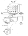
- Fig. 9 shows perspective views of an image memory and display memories shown in Fig. 8;
- Fig. 10 is a flowchart for explaining the procedures for transfer and display in the consecutive image processing system shown in Fig. 8;
- Fig. 11 is a schematic block diagram of a consecutive image processing system according to still another embodiment of the present invention;
- Fig. 12 shows perspective views of an image memory and display memories shown in Fig. 11;
- Fig. 13 is a flowchart of the transfer and display procedure in the consecutive image processing system shown in Fig. 11; and
- Fig. 14 shows display memories according to still another embodiment of the present invention.
- Before describing the preferred embodiments, an explanation will be given of conventional consecutive image processing methods and the problems thereof, for reference.
- In Fig. 1,
reference numbers 11 to 13 represent display memories provided in the image display apparatus. Each memory is divided into four memory areas, and each memory area corresponds to each memory frame in the memory control apparatus. That is, the content of each frame is transferred to the corresponding memory area of the display memory, and the content of the memory area is then displayed on the display device. In this case, the numbering of thememory areas 1 to 12 denotes the order in which the memory areas are displayed. - When the content of the
memory area 1 of thememory 11 is displayed on the display device, a start address of thearea 1 is designated and thememory 11 is selected. After display, thememory area 1 is switched to thememory area 2, in order to display the content of thememory area 2. In this case, only a "memory switch" is performed because the start address is the same in thismemory 11. After display, thememory area 2 is switched to thememory area 3, to display the content of thememory area 3. In this case also, only a "memory switch" is performed. - After displaying the content of the
memory area 3, thememory area 3 is switched to thememory area 4 in thememory 11. In this case, it is necessary to switch the start address to a new start address of thememory area 4, in correspondence with the memory switch. - There are, however, problems in the switching of the memory area and start address. That is, when the start address is switched to the new start address after switching the memory, the content of the
memory area 1, which is now unwanted, is temporarily displayed on the display device. This is because the timing of memory switch is earlier than that of the start address. - In Fig. 2,
reference number 21 represents an image memory in the image control apparatus, 22 a display memory in the image display apparatus, and 23 a display section in the image display apparatus. A display enlargement rate is designated from the image control apparatus side to the image display apparatus side. In this case, the contents of the image memory consisting of 512 x 512 x 8 (bits) are transferred to and stored in the memory area at the same size as that of the frame in the display memory consisting of 1024 x 1280 x 8 (bits). This stored image is enlarged in accordance with the predetermined rate (in this case, x 2) and displayed on the display device. - However, problems occur when the image data is transferred from the control apparatus to the display apparatus. That is, this transfer is performed by only one display memory and by sequential transmission of every picture element. Therefore, as is obvious, a longer transmission time is needed to transfer the image data.
- In Fig. 3,
reference number 31 corresponds to referencenumber - Accordingly, the same problem as in the case of Fig. 2 arises; that the transfer time is too long.
- A consecutive image processing system according to the present invention will be explained in detail hereinafter.
- In Fig. 4, the consecutive image processing system according to an embodiment of the present invention comprises a
host computer 41, animage control apparatus 42, and animage display apparatus 43. - The
image control apparatus 42 comprises animage memory 421 constituted by three random access memories (RAM's) each storing a number of image frames, a first microprocessor unit (MPU) 422 for controlling the data transmission between thehost computer 41 and theimage display apparatus 43, and for controlling read/write operations at theimage memory 421, and a memory transmission unit (MTU) 423 for transferring the content of theimage memory 421 to theimage display apparatus 43. - The
image memory 421 is constituted by threeimage memory units memory units host computer 41 through a bus line B. The bus line B includes a data bus line and address bus line, and accordingly, it is possible to access any memory area from 1 to 12 and read out the data therein based on a control program from thehost computer 41. - The microprocessor unit (MPU) 422 in the
image control apparatus 42 can control the start address of each memory area, can control the transfer of a light and shade signal obtained from each picture element to thehost computer 41 and theimage display apparatus 43, and can control the write-in of the light and shade signal to the memory area of the designated address. For example, the MPU.422 also can control the write-in of a digital image signal input from-an image input apparatus (not shown) by bypassing thehost computer 41 to theimage memory 421 and using a direct memory access (DMA) method. Accordingly, theMPU 422 generates a signal to ensure the data transmission/reception to and at the image input apparatus (not shown) and theimage display apparatus 43. - In the DMA transmission, the
first MPU 422 generates a DMA request signal to thehost computer 41. When thefirst MPU 422 receives a DMA acknowledgement signal, the MPU 422 performs an address counter control and a memory chip enable control for storing the digital signal transferred from the image input apparatus in the memory area in theimage memory 421. Further, thefirst MPU 422 generates a control signal for transmission/ reception to and at asecond MPU 432 in theimage display apparatus 43, to transfer an image data of theimage memory 421 to thecorresponding display memory 431. - For example, the
MPU 422 also generates an initial address for DMA transmission, and performs a control for the acknowledgement signal corresponding to the request signal from theMPU 432 after the content of the memory designated by the address is latched and prepared in thememory transfer unit 423. After this control, theMPU 422 performs the address counter control and the chip enable control (memory switch control) based on the initial address, and transfers the image signal to theimage display apparatus 43 through thememory transfer unit 423. - In this case, the
MPU 432 performs a transfer control and an address control so as to transfer the image data from theimage control apparatus 42 and store it in the corresponding memory area in thedisplay memory 431. Moreover, theMPU 422 performs an address read-out counter control and a memory switch control for various memories in order to transfer the image frame of the image memory 42l.and store it in the corresponding memory area in thedisplay memory 431. Similarly, theMPU 432 performs the chip enable control for a memory switch at the same time as the address counter control. - Provided in the
image display apparatus 43 are thedisplay memory 431, theMPU 432, and thememory switch unit 434. Thedisplay memory 431 is constituted by threedisplay memory units memory switch unit 434 is provided for controlling a memory switch when the data is read out from the image frame. That is, thememory switch unit 434 is connected to thedisplay memory 431 and is controlled by a memory switch control signal sent from theMPU 432. Thememory switch unit 434 is connected to an enlargement processing unit 435. - As explained above, when the image data is transferred from the
image memory 421 to thedisplay memory 431 through thememory transfer unit 423, the size of the image frame is reduced in order to raise the transfer coefficient. Accordingly, the enlargement processing unit 435 is used for enlarging the image frame based on a predetermined enlargement rate, and the output of the enlargement processing unit 435 is applied to adisplay section 436. Thedisplay section 436 includes adisplay processing unit 436a and a display device (CRT) 436b. - The enlargement rate necessary for the enlargement processing unit 435 is sent from the
MPU 432. This enlargement rate is sent from thehost computer 41 to theMPU 432 through theMPU 422. In thisdisplay section 436, a display start command is sent from theMPU 422 to theMPU 432, and when an address for starting the image display is generated in theMPU 432, the image is displayed on the display device 436b through the display processing unit 435a. Moreover, aclock timer 433 is provided in theimage display apparatus 43". Thistimer 433 is used for asynchronously counting the waiting time from a read-out of the image data of thedisplay memory 431 until a display of the image on the display device 436b.. - The operation of the memory switch in the above-explained consecutive image processing system according to one embodiment of the present invention will be explained in detail hereinafter.
- In Fig. 5, three
display memories image memory units image control apparatus 42. Eachdisplay memory display memory display memory unit 431a stores the R picture element, 431b stores the G picture element, and 431c stores the B picture element. In this case, as explained hereinafter, when a look-up table (LUT) is used for the memory switch, the data in the LUT is displayed by a pseudo- color. - As shown in Fig. 5, the
frame 1 is provided in thesame memory 431c as theframe 3, and theframe 7 is provided in thesame memory 431a as theframe 6. Accordingly, it is not necessary to switch thedisplay memory 431c when the content of theframe 4 is displayed after displaying theframe 3. The relationship betweenframes - This operation will be explained in detail with reference to Figs. 5, 6A, and 6B.
- First, the memory area 1 (frame 1) in the
memory 431a is accessed and.displayed on the display device. Next, thememory 431b is designated and a memory switch is made from thememory 431a to thememory 431b, and thememory area 2 is accessed and displayed on the display device. Next, thememory 431c is designated and a memory switch is made from thememory 431b to thememory 431c, and thememory area 3 is accessed and displayed on the display device. - Next, as the feature of the present invention, when the
area 4 is displayed, a memory switch is not necessary. In this case, only the address is switched to the start address of thearea 4, and after the start address is switched, thearea 4 is accessed and displayed on the display device. Next, thememory 431b is designated and a memory switch is made from thememory 431c to thememory 431b, and thearea 5 is accessed and displayed on the display device. Regarding the memory switch and frame switch from thearea 6 to thearea 7 and other frames, the control is carried out by the same procedure. Finally, the display on the display device is ended after thearea 12 in thememory 431a is displayed. - The above-explained procedures are shown in Fig. 6A, and the conventional procedures are shown in Fig. 6B. In these drawings,
reference numbers 1 to 5 denote frame numbers to be displayed, M1 to M5 denote timings of the memory switch, A1 and A2 denote timings of the start address switch, and T1 to T4 denote the ON timing of the timer. In Fig. 6A, when the memory switch M3 is made, theframe 3 is displayed during the time T3. After this time, an address switch is made, and theframe 4 is displayed without a memory switch. In Fig. 6B, when a memory switch M3 is made, theframe 3 is displayed during a time T3. After this time, a memory switch M4 is made. In this case, theframe 1 is temporarily displayed because an address switch has not been made at that time. When an address switch A2 is made, theframe 4 is displayed during a time T4. Consequently, as explained in Fig. 6B, an undesirable display temporarily appears on the display device. - In Figs. 7A and 7B when the operation is started in the consecutive image processing system, the
MPU 422 transfers four.frames corresponding to fourmemory areas memory 421a to theimage display apparatus 43 through the memory transfer unit 423 (step Sl). TheMPU 432 controls the transferred data and writes the image frames into the corresponding memory area in the display memory. In this case, since theMPU 422 controls the address space equal to the frame size from the start address in theimage memory 421a by using only the address counter, it is not necessary to perform a memory switch control. Similarly, in theimage display apparatus 43, theMPU 432 generates the start address corresponding to the memory area, and thus it is not necessary to perform the memory switch control since theMPU unit 432 controls the write operation by sequentially generating addresses from the address space corresponding to each frame. - When the image transmission/reception with regard to the
memory 421a is performed, theMPU 422 switches the image memory from thememory 421a to thememory 421b, and th frames of memory areas in theimage memory 421b are transferred to the image display apparatus (step S2). The content of the memory is then stored in the corresponding memory area in theimage display apparatus 43. The same procedures as described above are performed regarding theimage memory 421c (step S3). - Based on the above-explained procedures, first, the
MPU 422 performs a memory switch after controlling the address counter to four frames, second, theMPU 422 controls the memory area in theimage memory 421b by controlling the address counter, and finally, theMPU 422 controls the memory area in the image memory 42lc by controlling the address counter after the memory switch. The write operations to thedisplay memory 431 are performed in the.same way as the above by theMPU 432. That is, theMPU 432 performs the address control of the memory area in thememory 431a, performs a memory switch to the memory area in thememory 431b, and then controls the address of the memory area, and finally, performs a memory switch to the memory area in the memory 43lc and then controls the address of the memory area. By the above-explained procedures, all contents in thememory areas 1 to 12 shown in Figs. 4 and 5 can-be transferred from theimage memory 421 to thedisplay memory 431. - After these procedures, the
MPU 422 transfers the enlargement rate data to the MPU 432 (step S4), and perform a display designation of thememory 421a. When theMPU 422 performs the display designation of thememory 421a, theMPU 432 designates thedisplay memory 431a and sends a control signal for a memory switch to thememory switch unit 434. Thememory switch unit 434 outputs the frames of thememory area 1 in thememory area 431a and then these outputs are enlarged in the enlargement processing unit 435 (step S6). After enlargement, theMPU 422 commands a display start designation, then theMPU 432 activates thedisplay processing unit 436a, and thus thedisplay processing unit 436a controls the frames of the memory areas in thememory 431a and displays them on thedisplay device 436a (steps S7 and S8). - The
MPU 432 also activates thetimer 25, and waits until thememory area 1 is displayed on the display device 436b. After the desired time has lapsed (step S9), theMPU 432 judges whether or not all frames are displayed (step S10). When thememory area 2 in thememory 431b and thememory area 3 in thememory 431c have not yet been displayed, although thememory area 1 is in thememory 431a, theMPU 432 performs the display designation of the next memory (step Sll) shown by the route A. That is, when theMPU 432 generates the start address designating thememory area 2 of thememory 431b, theMPU 432 performs the display based'on the display start designation signal. After confirming the finish of the timer operation, when thememory area 2 is displayed, theMPU 432 performs a memory switch to thememory 431c and thememory area 3 in the memory:431c is displayed. After passing this route A, theMPU 432 designates the final address of thememory area 3 in thememory 431c. - In the present invention, the MPU's 422 and 432 do not perform a memory switch in the next procedure, and only an address switch is performed from the
memory area 3 to thememory area 4 in thememory 431c. That is, only a start address conversion is performed (step S12). TheMPU 432 judges whether or not the display of thememory area 1 is finished (step S13). At this step, since the display is performed for thememory area 3, the display finish of thememory 431a becomes "NO" ("NO" at step S13). Accordingly, theMPU 422 sends a command for the display start to theMPU 432, and when theMPU 432 activates thedisplay processing unit 436, thememory area 4 of thememory 431c is displayed on the display device. The timer connected to the 432 counts the lapse of time, thenext memory area 2 is designated after the timer operation is finished, and theMPU 432 again judges whether or not the display of thememory 431 is finished (step S14). Since the memory 43la is not accessed, thememory area 5 of the memory 43lb is accessed and displayed after designating the display start and controlling the display process. During this time, thetimer 433 counts the lapse of time, and thememory 431a is accessed after the count by thetimer 433 is finished (step S15). Since the display of thememory 431a is not displayed, theMPU 432 performs the display start designation and thememory area 6 of thememory 431a is displayed. - The
timer 25 counts the lapse time during this time, and theMPU 432 judges whether or not the display of thememory area 1 is finished after the timer count is finished. At this time, since thememory area 6 of thememory 431a is already displayed, "YES" is selected (step S18). Next, the judgement is made of whether or. not the operation is finished. Since the operation is not finished, a next address designation is performed (step S19). That is, the memory switch from thememory 431a to the other memory is not performed, and theMPU 432 performs the address conversion so as to designate thememory area 7 of thememory 431a. That is, the route B is selected. The procedures after displaying thememory area 7 are the same as that for thememory areas 1 to 3. After displaying thememory area 9, only the address switch is performed to thememory area 10 in thememory 431c, and after displaying thememory area 12, the display on the display device can be smoothly finished. - In Fig. 8, the
image control apparatus 82 comprises animage memory 821 consisting of a RAM and divided into fourmemory areas 1 to 4, anMPU 822 for controlling the data transfer between thehost computer 81 and theimage control apparatus 82 and for controlling read/write operations from and to theimage memory 821, a memory transfer unit (MTU) 824 for controlling the transfer of the frames in theimage memory 821 to animage display apparatus 83, and atimer 823. - The
image memory 821 is divided into, for example, sixteenmemory areas 1 to 16, so as to store sixteen frames as shown in Fig. 9. In Fig. 8, only fourframes 1 to 4 are shown in theimage memory 821 to simplify .the explanation thereof. - The
image display apparatus 83 comprises twodisplay memories memory switch unit 833 for selecting the memory area designated by theMPU 832. That is, thememory switch unit 833 is connected to the output of thedisplay memory 831 and is controlled by a memory switch control signal from theMPU 832. The output of thememory switch unit 833 is connected to theenlargement processing unit 834 for enlarging the image data to be displayed. - In this embodiment, the image data in the
image memory 821 is alternately transferred to thedisplay memories MPU 822. Moreover, in this embodiment, it is possible to freely switch the memory size, and it is also possible to smoothly display consecutive images for the "loop-movie" technique by providing a plurality of display memories in the image display apparatus. - In Fig. 9, the
image memory 821 is divided into, for example, sixteen memory areas (frames) 1 to 16. The light and shade signal for each picture element is composed of eight bits. Accordingly, theimage memory 821 is constituted by 2048 x 2048 x 8 (bits) as the memory size. Each memory area comprises 512 x 512 x 8 (bits). In the image display apparatus, thedisplay memory 831 comprises at least twodisplay memory units memory unit 831a and 83lb comprises 1024 x 1280 x 8 (bits) as the memory size. These frames are alternately displayed on the display section after enlargement based on the predetermined enlargement rate. That is, first, theframe 831a is displayed as shown by the solid line, and second, theframe 831b is displayed as shown by the dotted line. - In this embodiment, first, the
image frame 1 of theimage memory 821 is transferred to thedisplay memory 831a as shown by thearrow 1, second, theframe 2 of theimage memory 821 is transferred to thedisplay memory 831b as shown by thearrow 2, third, theframe 831a is displayed on thedisplay section 835, and finally, theframe 831b is displayed on thedisplay section 835. At that time, when theframe 831b is read out and displayed, the next image frame 3-of theimage memory 821 is transferred to thedisplay memory 831a as shown by the dottedarrow 3. When theframe 831a is displayed, thenext image frame 4 of theimage memory 821 is transferred to thedisplay memory 831b as shown by the dottedarrow 4. As is obvious from the above-explanations, the display can be consecutively performed as a "loop-movie" display, since the frames are alternately transferred to the empty display memory side. - For example, when sixteen frames are transferred as shown in Fig. 9, first, the
frame 1 is transferred to thedisplay memory 831a, and then theframe 2 to thememory 831b. After transferring these frames, theframe 831a is enlarged and displayed, and then theframe 831b is also enlarged and displayed. Consequently, it is possible to obtain consecutive images as a "loop-movie" on thedisplay section 835. - In Fig. 10, when the image control apparatus and the image display apparatus are activated, the
MPU 822 transfers the enlargement rate value to the MPU 832 (step Sll). Next, theframe 1 of theimage memory 821 is transferred to thedisplay memory 831a (step S12). TheMPU 822 judges whether or not all transfers of the frames are finished (step S13). When all transfers are not finished, theframe 831a is enlarged and displayed on the display section (steps S14 and S15). During the above step, theeven number frame 2 of theimage memory 821 is transferred to thedisplay memory 831b (step S16). The transfer time is controlled by thetimer 823 and is judged whether or not it is finished (step S17). - When the
frame 2 of theimage memory 821 is transferred to the display memory and finished, theframe 2 of thedisplay memory 831b is enlarged by theenlargement processing unit 834 and is displayed by the display section 835 (steps S18 and S19). Next, theodd number frame 3 of.theimage memory 821 is transferred to thedisplay memory 831a (step S20). The transfer time is also controlled by the timer 823 (step S21). These procedures are repeated until theframe 16 of theimage memory 821 is transferred and displayed on thedisplay section 835. - In Fig. 11, the
image control apparatus 112 comprises animage memory 112a divided into a lower fourbits memory portion 1 and a upper fourbits memory portion 2, anMPU 112b for controlling the data transfer between thehost computer 111 and theimage control apparatus 112 and for read/write operations from and to the image memory l12a, a memory transfer unit (MTU) l12a for controlling the transfer of the frames in the image memory ll2a to animage display apparatus 113, atimer 112c for counting the transfer time, two look-up tables (LUT 1 and LUT 2) 112e and 112f for storing light and shade data of the image, and a look-up table transfer unit (TU) 112g for transferring the contents of the look-up tables 112e and 112f. - The image memory ll2a is divided into, for example, sixteen memory areas so as to store sixteen frames, and is also divided into two groups, i.e., the lower four
bits portion 1 and the upper fourbits portion 2, as shown in Fig. 12. - The
image display apparatus 113 comprises adisplay memory 113a also divided into lower and upper bits portions, anMPU 113b, and a selector unit 113c for selecting either the lower 4 bits portion or the upper 4 bits portion. The selector unit 113c is connected to the output of thedisplay memory 113a and is controlled by a control signal for selection from theMPU 113b. The selector unit 113c is connected to anenlargement processing unit 113d, and the enlargement processing unit l13d is connected to the display section l13e. Moreover, the image display apparatus l13 comprises two look-up tables (LUT 1 and LUT 2) 113f and 113g for storing light and shade data of the image and a look-up table switch unit (SWU) 113h for switching the look-up tables 113f and 113g. - The enlargement rate and memory switch command are sent from the
host computer 111 to theMPU 112b, and then sent from theMPU 112b to theMPU 113b. TheMPU 113b sends the enlargement rate data to theenlargement processing unit 113d. Thetimer 112c is used for asynchronously counting waiting times until the image frame in theimage memory 112a is read out and transferred to the display memory, and then displayed on the display section. - In this embodiment, each frame comprises four bits depth, and overlaps the other four bits frames as shown in Fig. 12. Briefly, the lower 4 bits frame is transferred to the
corresponding display memory 113a, and at the same time, the enlargement rate and LUT command are applied. When the lower 4 bits frame is displayed, the other image frame is transferred to the other display memory. As can be understood, when the lower 4 bits frame is displayed, the upper 4 bits frame is transferred from theimage memory 112a. These steps are alternately performed between the lower frame and upper frame by switching the look-up tables 1 and 2, and consecutive images as a "loop-movie" are obtained from these operations. - In Fig. 12, the
image memory 112a comprises 2048 x 2048 x (4 + 4) (bits) as the memory size. Each image frame is divided into a lower 4 bits portion (front half) and an upper 4 bits portion (rear half). Ac-cordingly, theimage memory 112a comprises substantially thirty-twoframes 1 to 32, and thedisplay memory 113a comprises 1024 x 1280 x (4 + 4) (bits) as the display memory size. In this embodiment, first, the front half portion of theframe 1 is transferred to the lower 4 bits area as shown by arrow① and the rear half portion of theframe 2 is transferred to the upper 4 bits area of thedisplay memory 113a. After transferring these frames, the transferred data is enlarged and displayed. The transfer and display are alternately performed by control of the look-up table (LUT 1 and LUT 2). - In Fig. 13, when the operation starts, the look-up table in the image control apparatus is switched to the LUT2 (step S31). next, the content of the LUT1 and the LUT2 is transferred to the image display apparatus through the
TU 112g (steps S32 and S33). Then the enlargement rate is transferred to the image display apparatus 113 (step S34) and the transfer image is enlarged (step S35). In this step, the transfer image is not displayed. Next, the lower bits memory corresponding to the LUTI is transferred to theimage display apparatus 113. In this step, the image is not displayed since the look-up table is not switched to the LUT1. The look-up table is then switched to the LUT1 (step S37), In this step, the image is displayed on the display device (step S38). They, the upper bits memory is transferred to the image display apparatus (step S39). The timer is then used to determine whether or not the display of the lower bits memory is finished, (step S40). When the timer count is finished the -look-up table is switched to the LUT2 (step S41) and the upper bits memory is displayed on the display device (step S42). Next, it is determined whether or not the display processing is finished (step S43). When the display processing is finished (YES), the procedure is completed (END). When the display processing is not finished, the lower bits memory is transferred (step S44). Next, it is determined whether or not the timer count is finished (step S45). When the timer count is finished, the flow is returned to step S37. - The embodiment shown in Fig. 14 is a combination of the above first and third embodiments. That is, each display memory is divided into, for example, four memory areas, and each of the four memory areas is divided into a lower-bits portion and an upper bits portion. Accordingly, for example, the display memory 141 is divided into a
lower bit portion 141a and anupper bit portion 141b, and each portion comprises four memory areas. The frame numbers indicate the order of display of the frames. - As is obvious, this embodiment include the merits of the above- two embodiments. That is, a memory switch, address switch, and LUT switch are smoothly performed, and thus it is possible to obtain consecutive images as a "loop-movie" in the consecutive image processing system.
Claims (10)
Applications Claiming Priority (6)
| Application Number | Priority Date | Filing Date | Title |
|---|---|---|---|
| JP61014444A JPS62172472A (en) | 1986-01-25 | 1986-01-25 | Successive picture processing system |
| JP61014443A JPH061488B2 (en) | 1986-01-25 | 1986-01-25 | Continuous image processing system |
| JP14443/86 | 1986-01-25 | ||
| JP14444/86 | 1986-01-25 | ||
| JP14442/86 | 1986-01-25 | ||
| JP61014442A JPS62172470A (en) | 1986-01-25 | 1986-01-25 | Successive picture processing system |
Related Child Applications (1)
| Application Number | Title | Priority Date | Filing Date |
|---|---|---|---|
| EP91102181.4 Division-Into | 1987-01-26 |
Publications (3)
| Publication Number | Publication Date |
|---|---|
| EP0232100A2 true EP0232100A2 (en) | 1987-08-12 |
| EP0232100A3 EP0232100A3 (en) | 1988-01-20 |
| EP0232100B1 EP0232100B1 (en) | 1991-12-11 |
Family
ID=27280642
Family Applications (2)
| Application Number | Title | Priority Date | Filing Date |
|---|---|---|---|
| EP19910102181 Withdrawn EP0439201A3 (en) | 1986-01-25 | 1987-01-26 | Consecutive image processing system |
| EP87300638A Expired - Lifetime EP0232100B1 (en) | 1986-01-25 | 1987-01-26 | Consecutive image processing system |
Family Applications Before (1)
| Application Number | Title | Priority Date | Filing Date |
|---|---|---|---|
| EP19910102181 Withdrawn EP0439201A3 (en) | 1986-01-25 | 1987-01-26 | Consecutive image processing system |
Country Status (4)
| Country | Link |
|---|---|
| US (1) | US4928253A (en) |
| EP (2) | EP0439201A3 (en) |
| AU (1) | AU577722B2 (en) |
| DE (1) | DE3775077D1 (en) |
Families Citing this family (27)
| Publication number | Priority date | Publication date | Assignee | Title |
|---|---|---|---|---|
| GB8626594D0 (en) * | 1986-11-07 | 1986-12-10 | Renishaw Plc | Rotary cutting tool |
| JP2933974B2 (en) * | 1990-04-06 | 1999-08-16 | キヤノン株式会社 | Print control apparatus and method |
| US5210825A (en) * | 1990-04-26 | 1993-05-11 | Teknekron Communications Systems, Inc. | Method and an apparatus for displaying graphical data received from a remote computer by a local computer |
| JPH0416996A (en) * | 1990-05-11 | 1992-01-21 | Mitsubishi Electric Corp | Display device |
| US5467444A (en) * | 1990-11-07 | 1995-11-14 | Hitachi, Ltd. | Method of three-dimensional display of object-oriented figure information and system thereof |
| US5293483A (en) * | 1990-11-30 | 1994-03-08 | Matsushita Electric Industrial Co., Ltd. | Combined image and control data image memory device |
| US5594849A (en) * | 1991-08-09 | 1997-01-14 | Yale University | Biomedical magnetism imaging apparatus and method |
| FR2697360B1 (en) * | 1992-10-26 | 1994-12-30 | Jeux Franc | Acquisition and playback system of a sequence of animated video images in real time. |
| US5345543A (en) * | 1992-11-16 | 1994-09-06 | Apple Computer, Inc. | Method for manipulating objects on a computer display |
| US5463739A (en) * | 1992-12-22 | 1995-10-31 | International Business Machines Corporation | Apparatus for vetoing reallocation requests during a data transfer based on data bus latency and the number of received reallocation requests below a threshold |
| US6108001A (en) * | 1993-05-21 | 2000-08-22 | International Business Machines Corporation | Dynamic control of visual and/or audio presentation |
| US6351261B1 (en) * | 1993-08-31 | 2002-02-26 | Sun Microsystems, Inc. | System and method for a virtual reality system having a frame buffer that stores a plurality of view points that can be selected and viewed by the user |
| US5752010A (en) * | 1993-09-10 | 1998-05-12 | At&T Global Information Solutions Company | Dual-mode graphics controller with preemptive video access |
| US5633654A (en) * | 1993-11-12 | 1997-05-27 | Intel Corporation | Computer-implemented process and computer system for raster displaying video data using foreground and background commands |
| US5511195A (en) * | 1993-11-12 | 1996-04-23 | Intel Corporation | Driver, computer-implemented process, and computer system for processing data using loadable microcode running on a programmable processor |
| TR27409A (en) * | 1993-11-26 | 1995-03-27 | Jeux Franc Des | A system for recording and playback of motion video image sequence in real time. |
| US5537156A (en) * | 1994-03-24 | 1996-07-16 | Eastman Kodak Company | Frame buffer address generator for the mulitple format display of multiple format source video |
| US7843497B2 (en) | 1994-05-31 | 2010-11-30 | Conley Gregory J | Array-camera motion picture device, and methods to produce new visual and aural effects |
| US5574798A (en) * | 1994-08-03 | 1996-11-12 | International Business Machines Corporation | Visual presentation system which determines length of time to present each slide or transparency |
| US5608538A (en) * | 1994-08-24 | 1997-03-04 | International Business Machines Corporation | Scan line queuing for high performance image correction |
| US5717468A (en) * | 1994-12-02 | 1998-02-10 | International Business Machines Corporation | System and method for dynamically recording and displaying comments for a video movie |
| US20040139481A1 (en) * | 2002-10-11 | 2004-07-15 | Larry Atlas | Browseable narrative architecture system and method |
| US7904812B2 (en) | 2002-10-11 | 2011-03-08 | Web River Media, Inc. | Browseable narrative architecture system and method |
| WO2004075120A2 (en) * | 2003-02-21 | 2004-09-02 | Koninklijke Philips Electronics N.V. | Caching for volume visualization |
| JP4683384B2 (en) | 2004-09-22 | 2011-05-18 | 株式会社ソニー・コンピュータエンタテインメント | Memory control method, graphic processor, and information processing apparatus |
| US8107116B2 (en) * | 2006-05-18 | 2012-01-31 | Konica Minolta Business Technologies, Inc. | Image forming apparatus |
| CN105739934B (en) * | 2014-12-11 | 2018-09-21 | 华为终端(东莞)有限公司 | Multi-screen splicing display processing method and equipment |
Citations (2)
| Publication number | Priority date | Publication date | Assignee | Title |
|---|---|---|---|---|
| EP0136652A2 (en) * | 1983-09-30 | 1985-04-10 | Kabushiki Kaisha Toshiba | Image processing apparatus with automatic window processing function |
| EP0137481A2 (en) * | 1983-10-11 | 1985-04-17 | Hitachi, Ltd. | Image processing system |
Family Cites Families (9)
| Publication number | Priority date | Publication date | Assignee | Title |
|---|---|---|---|---|
| FR2468264A1 (en) * | 1979-10-18 | 1981-04-30 | Materiel Telephoniqu Thomson C | SYSTEM FOR DIGITIGLY PRODUCING IMAGES PROVIDED WITH IDENTICAL TARGETS FOR ELECTRONIC INCRUSTATION IN A LANDSCAPE IMAGE |
| JPS57190995A (en) * | 1981-05-20 | 1982-11-24 | Mitsubishi Electric Corp | Display indicator |
| JPS58159184A (en) * | 1982-03-17 | 1983-09-21 | Nec Corp | Picture turning device |
| US4723226A (en) * | 1982-09-29 | 1988-02-02 | Texas Instruments Incorporated | Video display system using serial/parallel access memories |
| US4800380A (en) * | 1982-12-21 | 1989-01-24 | Convergent Technologies | Multi-plane page mode video memory controller |
| US4823119A (en) * | 1982-12-22 | 1989-04-18 | Tokyo Shibaura Denki Kabushiki Kaisha | Pattern write control circuit |
| JPS59180871A (en) * | 1983-03-31 | 1984-10-15 | Fujitsu Ltd | Semiconductor memory device |
| US4595917A (en) * | 1983-06-13 | 1986-06-17 | Vectrix Corporation | Data processing technique for computer color graphic system |
| US4755810A (en) * | 1985-04-05 | 1988-07-05 | Tektronix, Inc. | Frame buffer memory |
-
1987
- 1987-01-21 US US07/005,776 patent/US4928253A/en not_active Expired - Fee Related
- 1987-01-23 AU AU67964/87A patent/AU577722B2/en not_active Ceased
- 1987-01-26 DE DE8787300638T patent/DE3775077D1/en not_active Expired - Fee Related
- 1987-01-26 EP EP19910102181 patent/EP0439201A3/en not_active Withdrawn
- 1987-01-26 EP EP87300638A patent/EP0232100B1/en not_active Expired - Lifetime
Patent Citations (2)
| Publication number | Priority date | Publication date | Assignee | Title |
|---|---|---|---|---|
| EP0136652A2 (en) * | 1983-09-30 | 1985-04-10 | Kabushiki Kaisha Toshiba | Image processing apparatus with automatic window processing function |
| EP0137481A2 (en) * | 1983-10-11 | 1985-04-17 | Hitachi, Ltd. | Image processing system |
Non-Patent Citations (1)
| Title |
|---|
| "A Practical Course on Operating Systems", C. J. Theakes and G. R. Borrkes, 1983, Mac Millan, London, pages 37 - 38. * |
Also Published As
| Publication number | Publication date |
|---|---|
| EP0439201A3 (en) | 1993-08-04 |
| DE3775077D1 (en) | 1992-01-23 |
| EP0232100B1 (en) | 1991-12-11 |
| US4928253A (en) | 1990-05-22 |
| AU6796487A (en) | 1987-07-30 |
| EP0232100A3 (en) | 1988-01-20 |
| AU577722B2 (en) | 1988-09-29 |
| EP0439201A2 (en) | 1991-07-31 |
Similar Documents
| Publication | Publication Date | Title |
|---|---|---|
| US4928253A (en) | Consecutive image processing system | |
| US4799053A (en) | Color palette having multiplexed color look up table loading | |
| US4620289A (en) | Video display system | |
| EP0454414B1 (en) | Video signal display | |
| US6049360A (en) | Image composing and displaying method and apparatus | |
| US6157374A (en) | Graphics display system and method for providing internally timed time-varying properties of display attributes | |
| EP0525943A2 (en) | Method and apparatus for merging independently generated internal video signal with external video signal | |
| US6753872B2 (en) | Rendering processing apparatus requiring less storage capacity for memory and method therefor | |
| GB2231245A (en) | Apparatus for selecting mode of output in a computer system | |
| GB2226938A (en) | Video display apparatus | |
| GB2137857A (en) | Computer Graphics System | |
| JPH0876713A (en) | Display controller | |
| JPH06314085A (en) | Image processing system | |
| US5517609A (en) | Graphics display system using tiles of data | |
| US5610630A (en) | Graphic display control system | |
| EP0887768A2 (en) | A graphic processor and a graphic processing method | |
| GB2230924A (en) | Improved apparatus for rapidly clearing the output display of a computer system | |
| US5943102A (en) | Image data decoding method and apparatus comparing decode and display progress | |
| CA2136478A1 (en) | Digital memory for display system using spatial light modulator | |
| JPH0454789A (en) | Television picture display device | |
| US5519413A (en) | Method and apparatus for concurrently scanning and filling a memory | |
| US6897874B1 (en) | Method and apparatus for providing overlay images | |
| EP0474366B1 (en) | Graphics display system including a video random access memory with a split serial register and a run counter | |
| US5646694A (en) | Moving picture decoding apparatus having three line buffers controlled to store and provide picture data of different resolutions | |
| JPS62172470A (en) | Successive picture processing system |
Legal Events
| Date | Code | Title | Description |
|---|---|---|---|
| PUAI | Public reference made under article 153(3) epc to a published international application that has entered the european phase |
Free format text: ORIGINAL CODE: 0009012 |
|
| AK | Designated contracting states |
Kind code of ref document: A2 Designated state(s): DE FR GB |
|
| PUAL | Search report despatched |
Free format text: ORIGINAL CODE: 0009013 |
|
| AK | Designated contracting states |
Kind code of ref document: A3 Designated state(s): DE FR GB |
|
| 17P | Request for examination filed |
Effective date: 19880329 |
|
| 17Q | First examination report despatched |
Effective date: 19890706 |
|
| GRAA | (expected) grant |
Free format text: ORIGINAL CODE: 0009210 |
|
| AK | Designated contracting states |
Kind code of ref document: B1 Designated state(s): DE FR GB |
|
| XX | Miscellaneous (additional remarks) |
Free format text: TEILANMELDUNG 91102181.4 EINGEREICHT AM 26/01/87. |
|
| REF | Corresponds to: |
Ref document number: 3775077 Country of ref document: DE Date of ref document: 19920123 |
|
| ET | Fr: translation filed | ||
| PLBE | No opposition filed within time limit |
Free format text: ORIGINAL CODE: 0009261 |
|
| STAA | Information on the status of an ep patent application or granted ep patent |
Free format text: STATUS: NO OPPOSITION FILED WITHIN TIME LIMIT |
|
| PGFP | Annual fee paid to national office [announced via postgrant information from national office to epo] |
Ref country code: GB Payment date: 19921106 Year of fee payment: 7 |
|
| 26N | No opposition filed | ||
| PGFP | Annual fee paid to national office [announced via postgrant information from national office to epo] |
Ref country code: FR Payment date: 19921222 Year of fee payment: 7 |
|
| PGFP | Annual fee paid to national office [announced via postgrant information from national office to epo] |
Ref country code: DE Payment date: 19930323 Year of fee payment: 7 |
|
| PG25 | Lapsed in a contracting state [announced via postgrant information from national office to epo] |
Ref country code: GB Effective date: 19940126 |
|
| GBPC | Gb: european patent ceased through non-payment of renewal fee |
Effective date: 19940126 |
|
| PG25 | Lapsed in a contracting state [announced via postgrant information from national office to epo] |
Ref country code: FR Effective date: 19940930 |
|
| PG25 | Lapsed in a contracting state [announced via postgrant information from national office to epo] |
Ref country code: DE Effective date: 19941001 |
|
| REG | Reference to a national code |
Ref country code: FR Ref legal event code: ST |