EP0230847B1 - Packet multiplex switching system - Google Patents
Packet multiplex switching system Download PDFInfo
- Publication number
- EP0230847B1 EP0230847B1 EP86460024A EP86460024A EP0230847B1 EP 0230847 B1 EP0230847 B1 EP 0230847B1 EP 86460024 A EP86460024 A EP 86460024A EP 86460024 A EP86460024 A EP 86460024A EP 0230847 B1 EP0230847 B1 EP 0230847B1
- Authority
- EP
- European Patent Office
- Prior art keywords
- inputs
- outputs
- output
- outgoing
- time
- Prior art date
- Legal status (The legal status is an assumption and is not a legal conclusion. Google has not performed a legal analysis and makes no representation as to the accuracy of the status listed.)
- Expired - Lifetime
Links
Images


Classifications
-
- H—ELECTRICITY
- H04—ELECTRIC COMMUNICATION TECHNIQUE
- H04L—TRANSMISSION OF DIGITAL INFORMATION, e.g. TELEGRAPHIC COMMUNICATION
- H04L49/00—Packet switching elements
- H04L49/10—Packet switching elements characterised by the switching fabric construction
- H04L49/103—Packet switching elements characterised by the switching fabric construction using a shared central buffer; using a shared memory
-
- H—ELECTRICITY
- H04—ELECTRIC COMMUNICATION TECHNIQUE
- H04L—TRANSMISSION OF DIGITAL INFORMATION, e.g. TELEGRAPHIC COMMUNICATION
- H04L49/00—Packet switching elements
- H04L49/30—Peripheral units, e.g. input or output ports
- H04L49/3009—Header conversion, routing tables or routing tags
-
- H—ELECTRICITY
- H04—ELECTRIC COMMUNICATION TECHNIQUE
- H04L—TRANSMISSION OF DIGITAL INFORMATION, e.g. TELEGRAPHIC COMMUNICATION
- H04L49/00—Packet switching elements
- H04L49/40—Constructional details, e.g. power supply, mechanical construction or backplane
Definitions
- the present invention relates to a synchronous fixed length packet multiplex switching system.
- a switching system for multiplexing synchronous fixed length packets is already described in document FR-A-2 538 976.
- packets are considered as time slots with explicit addressing, which makes it possible to use them.
- the packet switching function essentially consists in associating with each incoming packet, identified by its multiplex number entering among several and its label, a new identification itself characterized by two attributes of the same type, that is to say a new label and number of the outgoing multiplex among several which will deliver the packet.
- the packet (e, i) is switched where e is the number of the incoming multiplex and the label, into an outgoing packet (s, j), where s is the number of the outgoing multiplex and the new label.
- a first action is taken on the packet (e, i) before its storage in the buffer memory, this action consisting of a "label conversion" which corresponds to a permutation of time interval in switching time of circuits.
- This conversion is carried out by a control memory, which has been programmed during the establishment of packet communication.
- the label ballast is replaced by the label j.
- the packet (e, j) is then stored in the buffer memory at a known address, a function of the writing instant defined by e. This address is stored in a queue associated with the outgoing multiplex.
- the queue associated with the outgoing multiplex s is explored to deliver the address of the next packet that the outgoing multiplex s will have to carry.
- the information forming the packet is stored in the buffer memory.
- Incoming packets first have their bytes converted in parallel, then pass through memories serving as queues which are produced by means of FiFo or "first in - first out" memories.
- the conventional series-to-parallel conversion of parallel byte queues is replaced by a succession of simultaneous permutations of parallel bytes for all of the incoming multiplexes and another succession of simultaneous permutations of parallel bytes for all of the outgoing multiplexes.
- the control logic which includes the only control memory, being able to analyze only one label per byte time, it is expected that the labels of the different packets are linked in a time-shifted manner. This is achieved by ensuring in the input queues a time difference of 1 byte from one queue to the next.
- a rotation matrix makes it possible to perform a controllable rotation on groups of n bytes. The order of rotation progresses by one step at each "byte time".
- the parallel-to-serial converter is itself formed by a cyclically controlled rotation matrix performing the shifts in the opposite direction to the input matrix.
- the number of bytes per packet that is to say per time interval, is equal to a power of 2 and, even more particularly, a number of bytes per packet equal to sixteen.
- Each packet of this type consists of a header, occupying one byte, followed by fifteen bytes of information.
- the number of information bytes is a power of 2.
- An object of the invention consists in providing a multiplex switching system for synchronous fixed-length packets, the number of information bytes of which is equal to a power of 2.
- packets consist of a header, occupying one byte, followed by 24 or sixteen bytes.
- the first conversion means comprise an input circuit with alignment file by incoming junction, the alignment files having their reference inputs connected respectively to the outputs of a demultiplexer whose input is connected to identification stages (e) of the time base counter, the read inputs of the alignment queues being respectively connected to the frame outputs of the time base register.
- the outputs of the input conversion means are, on the one hand, connected to the inputs of a rotation matrix with n no rotation, n outputs and n inputs, and, on the other hand, to the inputs of a multiplexer with n inputs and an output which is connected to address inputs of the control memory, the control input of the multiplexer and of the rotation matrix being connected to the identification stages of the counter of the time base and the multiplexer validation input being connected to the first stage of the counter.
- the data output from the control memory comprises as many wires as bits per header and n wires respectively connected to the write inputs of n address queues corresponding respectively to the n outgoing junctions, the inputs data of the address queues being connected to the stages of the counter.
- the output of the first elementary memory of the buffer memory is connected to a demultiplexer whose outputs connected to the first inputs of n multiplexers whose second inputs are connected to the outputs of a rotation matrix with n no rotation , n outputs and n inputs, the inputs of which are connected to the outputs of the last elementary memories of the buffer memory, the control inputs of the demultiplexer and of the rotation matrix being connected by inverters to the identification stages of the base counter of time, the control inputs of the n multiplexers being connected to the second stage of the counter and their outputs respectively connected to the data inputs of n queues whose write inputs are respectively connected to the frame outputs of the base register time, the n queues having their outputs respectively connected to the output junctions.
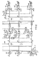
- FIG. 1 and 2 shows an exemplary embodiment of a switching matrix forming a basic element of a packet time switch according to the invention.
- Packets arriving on channels E1 to E16 are to be switched to be transmitted on channels S1 to S16.
- Each input channel E1 to E16, transmitting a bit stream is connected to the input of an input circuit CE1 to CE16.
- Each input circuit CE1 to CE16 consists of a serial-parallel converter operating byte by byte and a queue organized like the input circuit shown in FIG. 2 of document FR-A-2,538,976. We will therefore not give further details on these input circuits in the following.
- circuits CE1 to CE16 therefore serve to "align" the multiplexes.
- Each queue must have a size greater than seventeen nine-bit words, since we consider packets of seventeen eight-bit words and, in the queue, one bit is reserved to indicate the start of a packet .
- the circuits CE1 to CE16 constitute time-shifting means for the incoming multiplexes E1 to E16, so that the headers of the various multiplexes leaving the circuits CE1 to CE16 are delivered sequentially, in a diagonal alignment.
- each output f3.1 to f3.16 imposes the moment of reading of the first packet byte in the corresponding queue, that is to say the moment of reading of the label.
- the switching matrix also includes a time base BT, a circuit for switching and converting the label ACE, an input rotation matrix MRE, buffers MO and M1 to M16, an output rotation matrix MRS , output queues MS1 to MS16, parallel / serial converters p / s1 to p / s16, and ancillary addressing and switching circuits, which will appear in the following description.
- the BT time base is in particular provided for distributing the read clock signals HL1 to HL16 to the queues of the input circuits CE1 to CE16.
- the BT time base includes a ten-stage CTS binary counter at the input of which a clock signal of frequency 4H is applied, it being understood that 1 / H represents a byte time for each of the incoming or outgoing multiplexes.
- the first output 2H delivers a signal at the frequency 2H
- the second output H delivers a signal at the frequency byte H
- the next four outputs are grouped to form an e link
- the last four outputs, plus those of the e link are grouped together to form the K bond.
- the data outputs of circuits CE1 to CE16 are respectively connected to the inputs C1 to C16 of the input rotation matrix MRE, FIG. 2.
- the input rotation matrix MRE like the output rotation matrix MRS, can be constituted by circuits known in English terminology under the names of "Rotate matrix” or “Shift matrix” marketed in ECL technology 1 OOK under n ° 100158. These matrices can be produced with a command associated with inputs or associated with outputs. In document FR-A-2 238 976, the matrices are of the type controlled by the input.
- the input matrix is of the command type associated with the inputs, which explains that, for a series of addresses increasing regularly, a data output is successively connected to the inputs, for each input l 'index being that of the increasing address.
- the outputs D1 to D16 of the matrix MRE are respectively connected to the inputs of the buffer memories M1 to M16.
- the outputs of the input circuits CE1 to CE16 are still respectively connected to the inputs of a MET multiplexer with sixteen inputs, FIG. 1.
- the eight-wire output of the MET multiplexer is connected, via an RMA buffer register, to the first eight address inputs of a random access memory MC located in the routing and conversion circuit d 'ACE label.
- the function of the RMA register is to present the data applied to its entries for a longer period of time. Its role will appear more clearly below.
- the four-wire harness e leaving the CTS counter of the BT time base, transmits four bits and is connected to the control input of the AIG switch having the sixteen outputs f3.1 to f3.16.
- the rotation of the CTS counter results in the circulation, at frequency H, of a "1" on the outputs f3.1 to f3.16.
- the successive signals applied to the wires f3.1 to f3.16 as a function of the output of the counter CTS cause the read activations of the input circuits CE1 to CE16 to be sequential.
- the beam e is also connected to the control input of the MET multiplexer so that bytes of the packets leaving the input circuits can be transmitted sequentially to the memory MC.
- Four second memory address entries re MC are also connected to the beam e, via the buffer register RMA.
- the harness e is also connected to the control input CDE ensuring the shifts in the input rotation matrix MRE.
- the eight-wire link K is connected, on the one hand, to the inputs E of two multiplexers MXO and MX1, on the other hand, to the output address queue data inputs FS1 to FS16 and, finally, at the input of a +1 adder, which adds 1 to the address sent to it.
- the output of the adder +1 is connected, in parallel, by eight-wire links, to the inputs E of multiplexers MX2 to MX16. Note that the +1 adder is not essential. However, it makes it possible to maintain the oblique configuration of the packets in the memories M1 to M16, by compensating for the byte period which is used to analyze a label in the ACE circuit, FIG. 1.
- the output of the memory MC is connected by 24 wires to its output register R, the first eight outputs of which are connected by a link to the input of the buffer memory MO and the other 16 outputs of which are individually connected to the control inputs d of files FS1 to FS16.
- the clock input of register R is connected to the clock output H.
- the output of the memory MO is connected to the input of a demultiplexer DET, FIG. 2, via a CTRO transfer circuit, FIG. 1.
- the outputs of memories M1 to M16 are connected to transfer circuits CTR1 to CTR16, the outputs of which are respectively connected to the inputs F1 to F16 of the output rotation matrix MRS.
- the CTRO transfer circuit which can be identical to the transfer circuit shown in Fig. 9 of document FR-A-2,538,976, comprises a multiplexer with two groups of eight inputs, the first of which is connected to the output of the memory MO and the second of which is connected to a group of potentials corresponding to a predetermined binary word.
- the output of the multiplexer which is the output of the CTRO transfer circuit is connected to the input of the DET demultiplexer.
- the transfer circuit CRT1 can be identical to the transfer circuit shown in FIG. 10 0 of the aforementioned document. Its output is connected to the F1 input.
- the transfer circuits CTR2 to CTR16 have the same structure as the transfer circuit CTR1.
- the control inputs of the circuits CTRO to CTR16 are respectively connected to the corresponding outputs of a register RGV of sixteen bits, the circuits CTRO and CTR1 having their control inputs connected to a common output of RGV.
- the data input of the RGV register is connected to the output of an MGS multiplexer and its clock input receives the H clock.
- the MGS multiplexer has sixteen inputs which are respectively connected to the "File empty" output wires of the queues FS1 to FS16.
- the MGS control input is connected to the inverted e link.
- the outputs G1 to G16 of the MRS matrix are respectively connected to the first inputs of multiplexers MXS1 to MXS16 whose second inputs are respectively connected to the sixteen outputs of the DET demultiplexer and whose control inputs receive the signal at frequency H.
- the outputs of multiplexers MXS1 to MXS16 are respectively connected to the output junctions S1 to S16, by queues MS1 to MS16 and converters p / s1 to p / s16, in each case a queue being in series with a converter.
- the write clock inputs HE1 to HE16 of the queues MS1 to MS16 are respectively connected to the outputs HL1 to HL16 of the time base BT.
- the shift control input CDE of the MRS matrix receives the information of the link e after inversion of each of the bits in (four) inverters INV.
- the output of inverters INV is also connected, on the one hand, to a demultiplexer TR and, on the other hand, to the control input of an MFS multiplexer.
- the demultiplexer TR has sixteen individual outputs connected by individual wires to the read control inputs of the queues FS1 to FS16.
- the demultiplexer TR performs the decoding of the complement of the binary number transmitted by e into a read order delivered on the appropriate wire to trigger the reading of an address in one of the queues FSI to FS16.
- the data outputs of address queues FS1 to FS16 are connected by sixteen links LS1 to LS16, with eight wires each, to the corresponding inputs of the MFS multiplexer.
- the eight-wire output of the MFS multiplexer is connected to the input of an ADL1 register counter.
- the eight-wire output of the counter-register ADL1 is connected, on the one hand, in parallel to the inputs L of the multiplexers MXO and MX1 and, on the other hand, to the input of a counter-register ADL2.
- the eight-wire output of the ADL2 register counter is connected, on the one hand, to the input L of the multiplexer MX2 and, on the other hand, to the input of a register counter according to ADL3, and so on. up to an ADL16 register counter.
- the register-counters ADL1 to ADL16 each have their counting or loading function selection input linked to the clock output H and their activation input of the selected function connected to the clock output 2H.
- the eight-wire outputs of the multiplexers MXO to MX16 are respectively connected to the address inputs of the memories MO to M16.
- the write / read E / L control inputs of the multiplexers MXO to MX16 are connected to the clock output H, making it possible to choose between the group associated with the input E, carrying write addresses, and the group associated with input L, carrying the reading addresses.
- the control input of the demultiplexer DET is connected to the link e by the inverters INV.
- the DET demultiplexer has sixteen eight-wire outputs which are respectively connected to the second inputs of the multiplexers MXS1 to MXS16, their selection being a function of the signal applied to the control input of the DET demultiplexer.
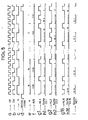
- the diagram in FIG. 5a represents the clock signal at the frequency 4H, which is transmitted by the clock circuit bearing the reference 4H.
- Diagrams 5b and 5c represent the output signals of the first two outputs of the CTS counter, i.e. say the signals whose frequencies are 2H and H, respectively.
- the diagram in FIG. 5d represents the output signal from the DECOD decoder.
- FIG. 5th the succession of numbers transmitted by the four-wire connection e.
- Fig. 5f we mentioned the succession of signals on the output wires of the AIG switch which are activated according to the numbers transmitted by the link e.
- Figs. 5g i , 5g 2 , ..., and 5g 16 represent the other output signals of the BT time base.
- the HL1 read clock signal is applied to the queue of the input circuit CE1.
- the packets leaving the circuit CE1 are shown, the order of the words being mentioned.
- the HL2 read clock signal applied to the queue of the input circuit CE2 is shown.
- the packets leaving the cirucit CE2 are shown, the word order being mentioned.
- the HL16 read clock signal applied to the queue of the input circuit CE16 is shown.
- Fig. 5:16 the packets leaving the circuit CE16 are shown, the order of the words being mentioned.
- each reading clock cycle is derived from a cycle with sixty-four elementary beats of which only seventeen are used.
- there are two instants of reading separated by an elementary time while then the instants of reading are separated by three elementary times.
- the cycles are successively shifted by four elementary times.
- Examination of Figs. 5h 1 to 5h 16 shows that with such read cycles, the structure of the packets delivered by the input circuits CE1 to CE16, is a diagonal structure similar to that which is shown in FIG. 5 of document FR-A-2 538 976 already mentioned.
- the MET multiplexer has its inputs successively activated by the numbers transmitted by the link e. Furthermore, the instants for writing to the memory register are shown in FIG. 5i. It appears that these times are chosen so that the MET multiplexer successively transmits the labels of channels 1 to 16 to the RMA register.
- the other circuits of the switch and label conversion unit ACE operating with a clock H with sixteen elementary times, each having a duration double of the clocks for reading the input circuits.
- the memory register RMA successively receives the labels and presents them to the memory MC for the entire duration of an elementary time of the clock H.
- the rotation addresses of the input rotation matrix MRE are determined by the beam e and allow the writing of the words of the packets, but not of the labels.
- the outputs D1 to D16 will respectively deliver the words 1 to 16 from the packets according to the configuration shown in FIG. 7.
- the output D1 applies to the memory M1 all the words 1
- the output D2 applies to the memory M2 all the words 2, etc.
- the memories M1 to M16, intended to record 16 ⁇ 16 packet fields are addressed on eight wires.
- the memory MC When the memory register RMA presents the label j at its output, the memory MC also receives the rank of the input junction concerned by the link e.
- the memory MC addressed by e and i, if i call a current label delivered by the multiplexer MET, delivers the new label and the identification of one or more suitable output junctions among the output junctions S1 to S16.
- the counter CTS delivers a number among 2 B , which represents the address Adi to which the label j must be written in the memory M0.
- this address Adi is introduced into each queue FS1 to FS16 which is designated by the value s of the output of the register R of the memory MC.
- the label is written in the memory MO.
- the beam K is also connected to the input E of the multiplexer MX1 used to address the memory M1, that is to say the address at which the first word of the packet following a label must be written in the memory M1.
- the writing takes place at the same time.
- the role of the +1 adder has already been described.
- Bytes 2 to 15 of the new label packet i are then successively written in the corresponding memories M2 to M16, the oblique configuration of FIG. 7 being respected.
- the memories MO to M16 are provided for recording 16 ⁇ 16 packets, which explains their addressing on eight wires.
- the time base Via the link e and the demultiplexer TR, the time base cyclically explores the sixteen queues FS1 to FS16.
- the information on the link e is also used to select the input of the MFS multiplexer which is connected to the queue selected by the demultiplexer TR.
- the inverters INV located upstream, on the one hand, of the input CDE of the output rotation matrix MRS and, on the other hand, of the control input of the demultiplexer DET, are intended to ensure a operation of this matrix in the opposite direction to the input matrix MRE, on the one hand, and to the multiplexer MET, on the other hand.
- the address Adi of the label of a packet is transmitted to the counter-register ADL1 whose output addresses, by MXO and MX1 respectively, the memories MO and M1 in reading.
- the content of the ADL1 register is incremented by 1.
- the ADL1 register counter transmits its content to the ADL2 register counter and receives from MFS a new address found in the queue. next. Therefore, at this instant, the content of the register ADL2 is capable, during the first half of the byte time, of addressing the memory M2 for reading, through MX2, that is to say of reading the second byte of the packet.
- the ADL2 register counter is incremented by 1, which will allow ADL3 to read byte 3 at the next time, etc. It therefore appears that the bytes of a packet are read simultaneously in the memories MO and M1, then in succession in the memories M2 to M16 where they occupy addresses varying from Adi to Ad (i + 15). Furthermore, the control information of the output rotation matrix MRS varying at each oc time tet, bytes "1" to "16" of a packet are successively delivered on the output Gs corresponding to the queue selected by the demultiplexer TR.
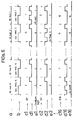
- Fig. 6a shows the series of translated labels delivered by the memory MO and respectively intended for the output channels S1 to S16.
- the translated label n ° 1 is intended for a packet applied to the channel S1, etc.
- Fig. 6b shows the frequency signal H which is applied to the control inputs of the multiplexers MXS1 to MXS16.
- Fig. 6 0 shows the sequence of words delivered by the G1 output of the MRS matrix. Since the control signal of the MXS1 multiplexer is the signal of FIG. 6b, it is understood that at each byte time, the multiplexer MXS1 lets pass, for half a time, the word applied by DET and in the other half time the word leaving G1. So in the time indicated by "Label translated 1" in FIG.
- FIG. 6di shows the write signal in the MS1 queue. It appears that all the words, plus the label are written in the queue as shown in Fig. 6th1.
- the operation which has just been described applies to the writes to the other queues MS2 to MS16, as shown in FIGS. 6c 2 , 6d 2 , 6th 2 , ..., 6C 16 , 6d 16 and 6th 16 .
- the signals of Figs. 6d 1 to 6d 16 are obviously supplied by the register REG of the time base BT.
- the control memory MC is a random access memory RAM 4Kx24 programmed from the outside by a control unit UCC. As we have seen, it assigns to each logical channel of an incoming multiplex a new label corresponding to the outgoing multiplex or outgoing multiplexes in which the queue or files FSi will be activated in writing in parallel according to the state of the 16 wires of control memory output.
- the address of the first byte of the packet in question, pointed to by the time base BT by the link K, is stored in the activated queue (s). It thus appears that the switching matrix of the invention can not only transmit point to point packets, but also makes it possible to broadcast them.
- the queues FS1 to FS16 When empty, the queues FS1 to FS16 have the value 0 at the data output. This means that no packet should be sent to the corresponding multiplex or what amounts to the same as the transmitted packet must have a null label, if it is desired, as mentioned in the preamble, to use the synchronization mode described in document EP-A-0 108 028.
- the "empty file” output wire of an Fsi file, validated by the demultiplexer TR is at "1" indicating that the queue is empty, the signal "1" appears at the output of the MGS multiplexer so that the first output wire of the RGV register is at 1 directing the CTRO multiplexer towards the potential bit "0".
- CTRO delivers a zero byte to the input of the DET demultiplexer.
- the first output wire of the register RGV at 1 directs the multiplexer of CTR1 towards alternating potentials of bits “1" and “0".
- the circuit CTR1 then delivers a byte of "1” and "0" to the input F1.
- the bit "1" of RGV progressed by one step and directs the multiplexers of the circuit CTR2, respectively to the potentials of bits “1” “and” 0 ". It delivers a byte of "1” “and” 0 "alternated at input F2, and so on at the following clock times up to the transfer circuit CTR16.
- switching matrices such as those which have just been described can be used to constitute switching stages or concentrators, as described in the document FR-A-2 538 976.
Description
La présente invention concerne un système de commutation de multiplex de paquets de longueur fixe synchrones.The present invention relates to a synchronous fixed length packet multiplex switching system.
A titre d'exemple, un multiplex de paquets de longueur fixe synchrones est décrit dans le document EP-A-0 108 028.By way of example, a multiplex of synchronous fixed length packets is described in document EP-A-0 108 028.
Un système de commutation de multiplex de paquets de longueur fixe synchrones est déjà décrit dans le document FR-A-2 538 976. Dans ce système les paquets sont considérés comme des intervalles de temps à adressage explicite, ce qui permet d'y utiliser des fonctions existantes dans les commutateurs temporels de circuits à commande par la sortie. La fonction commutation de paquets consiste essentiellement à associer à chaque paquet entrant, identifié par son numéro de multiplex entrant parmi plusieurs et son étiquette, une nouvelle identification elle-même caractérisée par deux attributs de même type, c'est-à-dire une nouvelle étiquette et le numéro du multiplex sortant parmi plusieurs qui va délivrer le paquet. Sous une autre forme, on commute le paquet (e, i) où e est le numéro du multiplex entrant et l'étiquette, en un paquet sortant (s, j), où s est le numéro du multiplex sortant et la nouvelle étiquette.A switching system for multiplexing synchronous fixed length packets is already described in document FR-A-2 538 976. In this system packets are considered as time slots with explicit addressing, which makes it possible to use them. existing functions in time switches of output-controlled circuits. The packet switching function essentially consists in associating with each incoming packet, identified by its multiplex number entering among several and its label, a new identification itself characterized by two attributes of the same type, that is to say a new label and number of the outgoing multiplex among several which will deliver the packet. In another form, the packet (e, i) is switched where e is the number of the incoming multiplex and the label, into an outgoing packet (s, j), where s is the number of the outgoing multiplex and the new label.
Dans cette commutation de paquets, une première action est entreprise sur le paquet (e, i) avant son rangement dans la mémoire tampon, cette action consistant en une "conversion d'étiquette" qui correspond à une permutation d'intervalle de temps en commutation temporelle de circuits. Cette conversion est effectuée par une mémoire de commande, qui a été programmée lors de l'établissement de la communication par paquets. Ainsi, l'étiquette lest remplacée par l'étiquette j. Le paquet (e, j) est alors rangé dans la mémoire tampon à une adresse connue, fonction de l'instant d'écriture défini par e. Cette adresse est stockée dans une file d'attente associée au multiplex sortants. Comme le système est commandé par la sortie, au cours du cycle d'exploration des multiplex sortant, la file d'attente associée au multiplex sortant s est explorée pour délivrer l'adresse du prochain paquet que le multiplex sortant s aura à porter. Comme en commutation temporelle de circuits, l'information formant le paquet est rangée dans la mémoire tampon.In this packet switching, a first action is taken on the packet (e, i) before its storage in the buffer memory, this action consisting of a "label conversion" which corresponds to a permutation of time interval in switching time of circuits. This conversion is carried out by a control memory, which has been programmed during the establishment of packet communication. Thus, the label ballast is replaced by the label j. The packet (e, j) is then stored in the buffer memory at a known address, a function of the writing instant defined by e. This address is stored in a queue associated with the outgoing multiplex. As the system is controlled by the output, during the exploration cycle of the outgoing multiplexes, the queue associated with the outgoing multiplex s is explored to deliver the address of the next packet that the outgoing multiplex s will have to carry. As in time circuit switching, the information forming the packet is stored in the buffer memory.
Plus particulièrement, dans ce système, la mise en parallèle de chaque paquet complet est effectuée avant l'écriture en mémoire tampon. Les paquets entrant ont d'abord leurs octets convertis en parallèle, puis transitent dans des mémoires servant de files d'attente qui sont réalisées au moyen de mémoires FiFo ou "premier entré - premier sorti.More particularly, in this system, the parallelization of each complete packet is carried out before writing into the buffer memory. Incoming packets first have their bytes converted in parallel, then pass through memories serving as queues which are produced by means of FiFo or "first in - first out" memories.
La conversion classique série-parallèle des files d'octets parallèles est remplacée par une succession de permutations simultanées d'octets parallèles pour l'ensemble des multiplex entrants et une autre succession de permutations simultanées d'octets parallèles pour l'ensemble des multiplex sortants. La logique de commande, qui comprend la seule mémoire de commande, n'étant capable d'analyser qu'une seule étiquette par temps d'octet, il est prévu que les étiquettes des différents paquets s'enchaînent de manière temporellement décalée. Ceci est obtenu en assurant dans les files d'attente d'entrée un déphasage temporel de 1 octet d'une file à la suivante. Une matrice de rotation permet d'effectuer une rotation commandable sur des groupes de n octets. L'ordre de la rotation progresse d'un pas à chaque "temps d'octet". En sortie de la matrice de rotation, les informations se présentent sous une forme dite "parallèle-diagonale". Les informations sont rangées sous cette forme dans la mémoire tampon. Le convertisseur parallèle-série est lui-même formé d'une matrice de rotation à commande cyclique effectuant les décalages dans le sens inverse de la matrice d'entrée.The conventional series-to-parallel conversion of parallel byte queues is replaced by a succession of simultaneous permutations of parallel bytes for all of the incoming multiplexes and another succession of simultaneous permutations of parallel bytes for all of the outgoing multiplexes. The control logic, which includes the only control memory, being able to analyze only one label per byte time, it is expected that the labels of the different packets are linked in a time-shifted manner. This is achieved by ensuring in the input queues a time difference of 1 byte from one queue to the next. A rotation matrix makes it possible to perform a controllable rotation on groups of n bytes. The order of rotation progresses by one step at each "byte time". At the output of the rotation matrix, the information is presented in a so-called "parallel-diagonal" form. The information is stored in this form in the buffer memory. The parallel-to-serial converter is itself formed by a cyclically controlled rotation matrix performing the shifts in the opposite direction to the input matrix.
Dans les exemples de réalisation du système de commutation décrit ci-dessus, on a, plus particulièrement, considéré le cas où le nombre d'octets par paquet, c'est-à-dire par intervalle de temps, est égal à une puissance de 2 et, encore plus particulièrement, un nombre d'octets par paquet égal à seize. Chaque paquet de ce type est constitué d'un en-tête, occupant un octet, suivi de quinze octets d'information. Or, dans certaines utilisations, il est préférable que le nombre des octets d'information soit une puissance de 2.In the exemplary embodiments of the switching system described above, we have more particularly considered the case where the number of bytes per packet, that is to say per time interval, is equal to a power of 2 and, even more particularly, a number of bytes per packet equal to sixteen. Each packet of this type consists of a header, occupying one byte, followed by fifteen bytes of information. However, in certain uses, it is preferable that the number of information bytes is a power of 2.
Un objet de l'invention consiste à prévoir un système de commutation de multiplex de paquets de longueur fixe synchrones, dont le nombre de multiplets d'information est égal à une puissance de 2. En pratique, bien que cet exemple ne soit pas limitatif, les paquets sont constitués d'un en-tête, occupant un octet, suivi de 24 ou seize octets.An object of the invention consists in providing a multiplex switching system for synchronous fixed-length packets, the number of information bytes of which is equal to a power of 2. In practice, although this example is not limiting, packets consist of a header, occupying one byte, followed by 24 or sixteen bytes.
Suivant une caractéristique de l'invention, il est prévu un système de commutation de multiplex à intervalles de temps contenant des paquets de longueur fixe provenant d'une pluralité de n jonctions entrantes vers une pluralité de n jonctions sortantes, chaque paquet entrant ou sortant comportant un en-tête plus n mots, le système comprenant:
- - des premiers moyens de conversion transformant les paquets série d'une pluralité de multiplex entrants, en paquets parallèles,
- - des moyens pour transmettre, aux entrées d'adresse d'une mémoire de commande, programmable à accès aléatoire, l'en-tête et l'identification de la jonction entrante d'origine de chaque paquet entrant, la sortie de données de ladite mémoire de commande délivrant un nouvel en-tête traduit affecté au paquet entrant parallèle en substitution de l'en-tête d'origine de manière à former, avec les n mots restants du paquet entrant, le paquet parallèle sortant,
- - une mémoire tampon activée cycliquement en écriture, pour mémoriser les paquets sortants,
- - des seconds moyens de conversion transformant chaque paquet parallèle sortant, lu dans la mémoire tampon, en un paquet série affecté au(x) multiplex destinataire(s),
- - une pluralité de moyens pour mémoriser les adresses des paquets qui sont présents dans la mémoire tampon, lesdits moyens étant validés sélectivement en écriture, en fonction d'une information fournie également par d'autres sorties de données de la mémoire de commande, chacun des moyens de mémorisation étant affecté de manière univoque à une jonction sortante, et
- - des moyens sensibles à un signal indiquant l'activation d'une quelconque des jonctions sortantes pour lire l'adresse contenue dans le moyen de mémorisation correspondant, de manière à retrouver, dans la mémoire tampon, le paquet sortant destiné à ladite jonction, le système comprenant encore:
- - une base de temps fonctionnant à un rythme double du débit mot des multiplex et délivrant n trames cycliques de 2n intervalles de temps chacune, chaque trame étant décalée de deux intervalles de temps par rapport à la précédente, chaque jonction entrante étant associée à une trame cyclique parmi n et chaque jonction sortante étant associée à une trame cyclique parmi n, le premier temps de chaque trame validant les moyens pour transmettre l'en-tête de la jonction entrante associée aux entrées d'adresse de la mémoire de commande dont la sortie de données est reliée à la première mémoire élémentaire de la mémoire tampon, les intervalles de temps suivants de rangs pairs validant successivement les entrées des n dernières mémoires élémentaires de la mémoire tampon, le premier intervalle de temps d'une trame validant la liaison entre la sortie de la première mémoire élémentaire et les seconds moyens de conversion vers la jonction sortante associée à ladite trame et les intervalles de temps suivants de rangs pairs validant les liaisons entre les sorties des n dernières mémoires et les seconds moyens de conversion vers ladite jonction sortante associée.
- first conversion means transforming the serial packets of a plurality of incoming multiplexes into parallel packets,
- means for transmitting, to the address inputs of a programmable control random access memory, the header and the identification of the original incoming junction of each incoming packet, the data output of said control memory delivering a new translated header assigned to the parallel incoming packet in substitution for the original header so as to form, with the n remaining words of the incoming packet, the outgoing parallel packet,
- - a buffer memory activated cyclically in writing, for memorizing outgoing packets,
- second conversion means transforming each outgoing parallel packet, read in the buffer memory, into a serial packet assigned to the recipient multiplex (s),
- a plurality of means for memorizing the addresses of the packets which are present in the buffer memory, said means being validated selectively in writing, as a function of information also supplied by other data outputs from the control memory, each of the memory means sation being unequivocally assigned to an outgoing junction, and
- means sensitive to a signal indicating the activation of any of the outgoing junctions to read the address contained in the corresponding storage means, so as to find, in the buffer memory, the outgoing packet intended for said junction, the system further comprising:
- - a time base operating at a rate double the word rate of the multiplexes and delivering n cyclic frames of 2n time intervals each, each frame being shifted by two time intervals compared to the previous one, each incoming junction being associated with a frame cyclic among n and each outgoing junction being associated with a cyclic frame among n, the first time of each frame validating the means for transmitting the header of the incoming junction associated with the address inputs of the control memory whose output of data is connected to the first elementary memory of the buffer memory, the following time intervals of even ranks successively validating the entries of the n last elementary memories of the buffer memory, the first time interval of a frame validating the connection between the output of the first elementary memory and the second conversion means to the outgoing junction associated with the adite frame and the following time intervals of even ranks validating the links between the outputs of the n last memories and the second conversion means to said associated outgoing junction.
Suivant une autre caractéristique, la base de temps est formée d'un compteur binaire cyclique à (K + 2) étages, où 2K représente les adresses de paquets de la mémoire tampon et où k est supérieur au logarithme du nombre de jonctions entrantes ou sortantes (e = log2 n), l'entrée d'horloge du compteur étant reliée à une horloge fonctionnant à quatre fois le rythme de débit mot des multiplex, les deux premiers étages délivrant les fréquences à la fréquence double du rythme mot et à la fréquence du rythme mot, les e étages suivants délivrant successivement les identifications des jonctions entrantes et sortantes, les sorties des (e+2) premiers étages étant reliés aux entrées d'un décodeur de valeur nulle dont la sortie est reliée à l'entrée d'initialisation d'un registre à décalage dont l'entrée d'horloge est reliée à l'horloge dont les entrées de chargement sont reliées à une série de potentiels logiques représentant la séquence binaire 1010100-010001...01000, la sortie du dernier étage du registre étant reliée à l'entrée de signal du premier, et les sorties des étages de rangs multiples de quatre délivrant les trames décalées.According to another characteristic, the time base is formed by a cyclic binary counter with (K + 2) stages, where 2K represents the addresses of packets of the buffer memory and where k is greater than the logarithm of the number of incoming or outgoing junctions (e = log 2 n), the clock input of the counter being connected to a clock operating at four times the word rate rhythm of the multiplexes, the first two stages delivering the frequencies at twice the frequency of the word rhythm and at frequency of the word rhythm, the following e stages successively delivering the identifications of the incoming and outgoing junctions, the outputs of the (e + 2) first stages being connected to the inputs of a decoder of zero value whose output is connected to the input d initialization of a shift register whose clock input is linked to the clock whose load inputs are linked to a series of logic potentials representing the binary sequence 1010100- 010001 ... 01000, the output of the last stage of the register being connected to the signal input of the first, and the outputs of the stages of multiple rows of four delivering the offset frames.
Suivant une autre caractéristique, les premiers moyens de conversion comprennent une circuit d'entrée à file d'alignement par jonction entrante, les files d'alignement ayant leurs entrées de référence reliées respectivement aux sorties d'un démultiplexeur dont l'entrée est reliée aux étages d'identification (e) du compteur de la base de temps, les entrées de lecture des files d'alignement étant respectivement reliées aux sorties de trame du registre de la base de temps.According to another characteristic, the first conversion means comprise an input circuit with alignment file by incoming junction, the alignment files having their reference inputs connected respectively to the outputs of a demultiplexer whose input is connected to identification stages (e) of the time base counter, the read inputs of the alignment queues being respectively connected to the frame outputs of the time base register.
Suivant une autre caractéristique, les sorties des moyens de conversion d'entrée sont, d'une part, reliées aux entrées d'une matrice de rotation à n pas de rotation, n sorties et n entrées, et, d'autre part, aux entrées d'un multiplexeur à n entrées et une sortie qui est reliée à des entrées d'adresse de la mémoire de commande, l'entrée de commande du multiplexeur et de la matrice de rotation étant reliées aux étages d'identification du compteur de la base de temps et l'entrée de validation du multiplexeur étant reliée au premier étage du compteur.According to another characteristic, the outputs of the input conversion means are, on the one hand, connected to the inputs of a rotation matrix with n no rotation, n outputs and n inputs, and, on the other hand, to the inputs of a multiplexer with n inputs and an output which is connected to address inputs of the control memory, the control input of the multiplexer and of the rotation matrix being connected to the identification stages of the counter of the time base and the multiplexer validation input being connected to the first stage of the counter.
Suivant une autre caractéristique, la sortie de données de la mémoire de commande comporte autant de fils que de bits par en-tête et n fils respectivement reliés aux entrées d'écriture de n files d'adresses correspondant respectivement aux n jonctions sortantes, les entrées de données des files d'adresses étant reliées aux étages du compteur.According to another characteristic, the data output from the control memory comprises as many wires as bits per header and n wires respectively connected to the write inputs of n address queues corresponding respectively to the n outgoing junctions, the inputs data of the address queues being connected to the stages of the counter.
Suivant une autre caractéristique, la sortie de la première mémoire élémentaire de la mémoire tampon est reliée à un démultiplexeur dont les sorties reliées aux premières entrées de n multiplexeurs dont les secondes entrées sont reliées aux sorties d'une matrice de rotation à n pas de rotation, n sorties et n entrées, dont les entrées sont reliées aux sorties des dernières mémoires élémentaires de la mémoire tampon, les entrées de commande du démultiplexeur et de la matrice de rotation étant reliées par des inverseurs aux étages d'identification du compteur de la base de temps, les entrées de commande des n multiplexeurs étant reliées au second étage du compteur et leurs sorties respectivement reliées aux entrées de données de n files d'attente dont les entrées d'écritures sont respectivement reliées aux sorties de trames du registre de la base de temps, les n files d'attente ayant leurs sorties respectivement reliées aux jonctions de sortie.According to another characteristic, the output of the first elementary memory of the buffer memory is connected to a demultiplexer whose outputs connected to the first inputs of n multiplexers whose second inputs are connected to the outputs of a rotation matrix with n no rotation , n outputs and n inputs, the inputs of which are connected to the outputs of the last elementary memories of the buffer memory, the control inputs of the demultiplexer and of the rotation matrix being connected by inverters to the identification stages of the base counter of time, the control inputs of the n multiplexers being connected to the second stage of the counter and their outputs respectively connected to the data inputs of n queues whose write inputs are respectively connected to the frame outputs of the base register time, the n queues having their outputs respectively connected to the output junctions.
Les caractéristiques de l'invention mentionnées ci-dessus, ainsi que d'autres, apparaîtront plus clairement à la lecture de la description suivante d'exemples de réalisation, ladite description étant faite en relation avec les dessins joints, parmi lesquels:
- les Figs. 1 et 2, assemblées comme l'indique la Fig. 3, forment le schéma d'une matrice de commutation suivant l'invention,
- la Fig. 4 est le schéma de la base de temps utilisée dans la matrice de commutation de la Fig. 1,
- les Figs. 5a à 5i sont des diagrammes temporels illustrant les lectures des paquets dans les circuits d'entrée de la matrice de commutation,
- les Figs. 6a à 6e sont des diagrammes temporels illustrant les écritures des paquets dans les files de sortie de la matrice de commutation, et
- la Fig. 7 est un diagramme illustrant la position des multiplex, sans leurs étiquettes, après passage dans la matrice de rotation d'entrée.
- Figs. 1 and 2, assembled as shown in Fig. 3, form the diagram of a switching matrix according to the invention,
- Fig. 4 is the diagram of the time base used in the switching matrix of FIG. 1,
- Figs. 5a to 5i are time diagrams illustrating the readings of the packets in the input circuits of the switching matrix,
- Figs. 6a to 6e are time diagrams illustrating the writes of the packets in the output queues of the switching matrix, and
- Fig. 7 is a diagram illustrating the position of the multiplexes, without their labels, after passing through the input rotation matrix.
Le bloc-diagramme des Figs. 1 et 2 montre un exemple de réalisation d'une matrice de commutation formant un élément de base d'un commutateur temporel de paquets suivant l'invention. Les paquets arrivant sur les canaux E1 à E16 sont à commuter pour être transmis sur les canaux S1 à S16. Chaque canal d'entrée E1 à E16, transmettant un train binaire, est relié à l'entrée d'un circuit d'entrée CE1 à CE16. Chaque circuit d'entrée CE1 à CE16 se compose d'un convertisseur série-parallèle fonctionnant octet par octet et d'une file d'attente organisés comme le circuit d'entrée montré à la Fig. 2 du document FR-A-2 538 976. On ne donnera donc pas, dans la suite, plus de détails sur ces circuits d'entrée.The block diagram of Figs. 1 and 2 shows an exemplary embodiment of a switching matrix forming a basic element of a packet time switch according to the invention. Packets arriving on channels E1 to E16 are to be switched to be transmitted on channels S1 to S16. Each input channel E1 to E16, transmitting a bit stream, is connected to the input of an input circuit CE1 to CE16. Each input circuit CE1 to CE16 consists of a serial-parallel converter operating byte by byte and a queue organized like the input circuit shown in FIG. 2 of document FR-A-2,538,976. We will therefore not give further details on these input circuits in the following.
Comme les jonctions E1 à E16, Fig. 2, sont reliées à des points d'origine différents, a priori non synchronisés, les étiquettes des paquets qu'elles transportent entrent à des temps d'octets différents dans les files d'attente des circuits d'entrée CE1 à CE16. Donc, initialement, les étiquettes des paquets n'ont aucune raison d'être lues dans un ordre prédéterminé aux sorties de ces files.Like the junctions E1 to E16, Fig. 2, are connected to different points of origin, a priori not synchronized, the labels of the packets which they transport enter at different byte times in the queues of the input circuits CE1 to CE16. Therefore, initially, the labels of the packets have no reason to be read in a predetermined order at the exits of these queues.
L'ensemble des files des circuits CE1 à CE16 sert donc à "aligner" les multiplex. Chaque file doit avoir une taille supérieure à dix-sept mots de neuf bits, puisque l'on considère des paquets de dix-sept mots de huit bits et que, dans la file, un bit est réservé pour indiquer le début d'un paquet. En pratique, les circuits CE1 à CE16 constituent des moyens de décalage dans le temps des multiplex entrants E1 à E16, de façon à ce que les en-têtes des différents multiplex sortant des circuits CE1 à CE16 soient délivrés séquentiellement, suivant un alignement diagonal.All the queues of circuits CE1 to CE16 therefore serve to "align" the multiplexes. Each queue must have a size greater than seventeen nine-bit words, since we consider packets of seventeen eight-bit words and, in the queue, one bit is reserved to indicate the start of a packet . In practice, the circuits CE1 to CE16 constitute time-shifting means for the incoming multiplexes E1 to E16, so that the headers of the various multiplexes leaving the circuits CE1 to CE16 are delivered sequentially, in a diagonal alignment.
En pratique, l'alignement diagonal des lectures dans les files est obtenu en utilisant des signaux de référence externes délivrés sur les fils f3.1 à f3.16 à partir d'un circuit d'aiguillage AIG. En ce qui concerne l'action de chaque signal de référence externe sur la file du circuit d'entrée correspondant, on se reportera à la Fig. 2 du document FR-A-2 538 976 et au texte qui l'a décrite. On retiendra que chaque sortie f3.1 à f3.16 impose le moment de lecture du premier octet de paquet dans la file correspondante, c'est-à-dire le moment de lecture de l'étiquette.In practice, the diagonal alignment of the readings in the queues is obtained by using external reference signals delivered on the wires f3.1 to f3.16 from an AIG switching circuit. With regard to the action of each external reference signal on the queue of the corresponding input circuit, reference is made to FIG. 2 of document FR-A-2 538 976 and the text which described it. It will be noted that each output f3.1 to f3.16 imposes the moment of reading of the first packet byte in the corresponding queue, that is to say the moment of reading of the label.
La matrice de commutation comprend encore une base de temps BT, un circuit d'aiguillage et de conversion d'étiquette ACE, une matrice de rotation d'entrée MRE, des mémoires tampons MO et M1 à M16, une matrice de rotation de sortie MRS, des files de sorties MS1 à MS16, des convertisseurs pa- rallèle/série p/s1 à p/s16, et des circuits annexes d'adressage et de commutation, qui apparaîtront dans la suite de la description.The switching matrix also includes a time base BT, a circuit for switching and converting the label ACE, an input rotation matrix MRE, buffers MO and M1 to M16, an output rotation matrix MRS , output queues MS1 to MS16, parallel / serial converters p / s1 to p / s16, and ancillary addressing and switching circuits, which will appear in the following description.
La base de temps BT, dont le schéma est montré à la Fig. 4, est notamment prévue pour distribuer les signaux d'horloge de lecture HL1 à HL16 aux files des circuits d'entrée CE1 à CE16. La base de temps BT, Fig. 2, comprend un compteur binaire CTS à dix étages à l'entrée duquel est appliqué un signal d'horloge de fréquence 4H, étant entendu que 1/H représente un temps d'octet pour chacun des multiplex entrants ou sortants. La première sortie 2H délivre un signal à la fréquence 2H, la seconde sortie H délivre un signal à la fréquence octet H, les quatre sorties suivantes sont groupées pour former une liaison e, les quatre dernières sorties, plus celles de la liaison e, sont groupées pour former la liaison K.The BT time base, the diagram of which is shown in FIG. 4, is in particular provided for distributing the read clock signals HL1 to HL16 to the queues of the input circuits CE1 to CE16. The BT time base, Fig. 2, includes a ten-stage CTS binary counter at the input of which a clock signal of
Les sorties 2H, H et e, c'est-à-dire les sorties transmettant le six bits de poids faiblè du compteur CTS, sont reliées aux entrées correspondantes d'un décodeur DECOD capable de décoder le mot 000000. La sortie du décodeur DECOD est reliée à l'entrée de validation de chargement L d'un registre à décalage REG à soixante-quatre bits. Le registre REG est rebouclé sur lui-même et a son entrée d'horloge de décalage qui reçoit le signal à la fréquence 4H. Aux entrées de chargement parallèle du registre REG, sont affectées les soixante-quatre valeurs binaires suivantes:
- 1010100010001000100010001000100010001000100 010001000100010001000
- Le registre a seize sorties parallèles HL16 à HL1 qui sortent respectivement des étages 4x1, 4x2, ... , 4x16 et qui sont respectivement reliées aux entrées de lecture des circuits d'entrées CE1 à CE16.
- 1010100010001000100010001000100010001000100 010001000100010001000
- The register has sixteen parallel outputs HL16 to HL1 which respectively exit from the stages 4x1, 4x2, ..., 4x16 and which are respectively connected to the reading inputs of the input circuits CE1 to CE16.
Les sorties de données des circuits CE1 à CE16 sont respectivement reliées aux entrées C1 à C16 de la matrice de rotation d'entrée MRE, Fig. 2. La matrice de rotation d'entrée MRE, comme la matrice de rotation de sortie MRS, peut être constituée par des circuits connus en terminologie anglo-saxonne sous les noms de "Rotate matrix" ou "Shift matrix" commercialisées en technologie ECL 1 OOK sous le n° 100158. Ces matrices peuvent être réalisées avec une commande associée aux entrées ou associée aux sorties. Dans le document FR-A-2 238 976, les matrices sont du type commandé par l'entrée. Dans le présent exemple de réalisation, la matrice d'entrée est du type à commande associée aux entrées, ce qui explique que, pour une suite d'adresses croissant régulièrement, une sortie de données se trouve reliée successivement aux entrées, pour chaque entrée l'indice étant celui de l'adresse croissante. Les sorties D1 à D16 de la matrice MRE sont respectivement reliées aux entrées des mémoires tampons M1 à M16.The data outputs of circuits CE1 to CE16 are respectively connected to the inputs C1 to C16 of the input rotation matrix MRE, FIG. 2. The input rotation matrix MRE, like the output rotation matrix MRS, can be constituted by circuits known in English terminology under the names of "Rotate matrix" or "Shift matrix" marketed in
Les sorties des circuits d'entrée CE1 à CE16 sont encore respectivement reliées aux entrées d'un multiplexeur MET à seize entrées, Fig. 1. La sortie à huit fils du multiplexeur MET est reliée, par l'intermédiaire d'un registre tampon RMA, aux huit premières entrées d'adresse d'une mémoire à accès aléatoire MC située dans le circuit d'aiguillage et de conversion d'étiquette ACE. Le registre RMA a pour fonction de présenter plus longtemps les données qui sont appliquées à ses entrées. Son rôle apparaîtra plus clairement dans la suite.The outputs of the input circuits CE1 to CE16 are still respectively connected to the inputs of a MET multiplexer with sixteen inputs, FIG. 1. The eight-wire output of the MET multiplexer is connected, via an RMA buffer register, to the first eight address inputs of a random access memory MC located in the routing and conversion circuit d 'ACE label. The function of the RMA register is to present the data applied to its entries for a longer period of time. Its role will appear more clearly below.
Le faisceau e à quatre fils, sortant du compteur CTS de la base de temps BT, transmet quatre bits et est relié à l'entrée de commande de l'aiguilleur AIG comportant les seize sorties f3.1 à f3.16. La rotation du compteur CTS se traduit par la circulation, à la fréquence H, d'un "1" sur les sorties f3.1 à f3.16. Les signaux successifs appliqués aux fils f3.1 à f3.16 en fonction de la sortie du compteur CTS font que les activations en lecture des circuits d'entrée CE1 à CE16 sont séquentielles. Le faisceau e est également relié à l'entrée de commande du multiplexeur MET si bien que des octets des paquets sortant des circuits d'entrée peuvent être transmis séquentiellement à la mémoire MC.The four-wire harness e, leaving the CTS counter of the BT time base, transmits four bits and is connected to the control input of the AIG switch having the sixteen outputs f3.1 to f3.16. The rotation of the CTS counter results in the circulation, at frequency H, of a "1" on the outputs f3.1 to f3.16. The successive signals applied to the wires f3.1 to f3.16 as a function of the output of the counter CTS cause the read activations of the input circuits CE1 to CE16 to be sequential. The beam e is also connected to the control input of the MET multiplexer so that bytes of the packets leaving the input circuits can be transmitted sequentially to the memory MC.
Quatre secondes entrées d'adresse de la mémoire MC sont également reliées au faisceau e, par l'intermédiaire du registre tampon RMA. Le faisceau e est encore relié à l'entrée de commande CDE assurant les décalages dans la matrice de rotation d'entrée MRE.Four second memory address entries re MC are also connected to the beam e, via the buffer register RMA. The harness e is also connected to the control input CDE ensuring the shifts in the input rotation matrix MRE.
La liaison K à huit fils est reliée, d'une part, aux entrées E de deux multiplexeurs MXO et MX1, d'autre part, aux entrées de données de files d'attente d'adresse de sortie FS1 à FS16 et, enfin, à l'entrée d'un additionneur +1, qui ajoute 1 à l'adresse qui lui est transmise. La sortie de l'additionneur +1 est reliée, en parallèle, par des liaisons à huit fils, aux entrées E de multiplexers MX2 à MX16. A noter que l'additionneur +1 n'est pas indispensable. Toutefois, il permet de maintenir la configuration oblique des paquets dans les mémoires M1 à M16, en compensant la période d'octet qui est utilisée pour analyser une étiquette dans le circuit ACE, Fig. 1.The eight-wire link K is connected, on the one hand, to the inputs E of two multiplexers MXO and MX1, on the other hand, to the output address queue data inputs FS1 to FS16 and, finally, at the input of a +1 adder, which adds 1 to the address sent to it. The output of the adder +1 is connected, in parallel, by eight-wire links, to the inputs E of multiplexers MX2 to MX16. Note that the +1 adder is not essential. However, it makes it possible to maintain the oblique configuration of the packets in the memories M1 to M16, by compensating for the byte period which is used to analyze a label in the ACE circuit, FIG. 1.
La sortie de la mémoire MC est reliée par 24 fils à son registre de sortie R dont les huits premières sorties sont reliées par un liaison à l'entrée de la mémoire tampon MO et dont les 16 autres sorties sont reliées individuellement aux entrées de commande d'écritures des files FS1 à FS16. L'entrée d'horloge du registre R est reliée à la sortie d'horloge H.The output of the memory MC is connected by 24 wires to its output register R, the first eight outputs of which are connected by a link to the input of the buffer memory MO and the other 16 outputs of which are individually connected to the control inputs d of files FS1 to FS16. The clock input of register R is connected to the clock output H.
La sortie de la mémoire MO est reliée à l'entrée d'un démultiplexeur DET, Fig. 2, par l'intermédiaire d'un circuit de transfert CTRO, Fig. 1. Les sorties des mémoires M1 à M16 sont reliées à des circuits de transfert CTR1 à CTR16 dont les sorties sont respectivement reliées aux entrées F1 à F16 de la matrice de rotation de sortie MRS.The output of the memory MO is connected to the input of a demultiplexer DET, FIG. 2, via a CTRO transfer circuit, FIG. 1. The outputs of memories M1 to M16 are connected to transfer circuits CTR1 to CTR16, the outputs of which are respectively connected to the inputs F1 to F16 of the output rotation matrix MRS.
Le circuit de transfert CTRO, qui peut être identique au circuit de transfert montré à la Fig. 9 du document FR-A-2 538 976, comprend un multiplexeur à deux groupes de huit entrées dont le premier est relié à la sortie de la mémoire MO et dont le second est relié à un groupe de potentiels correspondant à un mot binaire prédéterminé. La sortie du multiplexeur qui est la sortie du circuit de transfert CTRO est reliée à l'entrée du démultiplexeur DET.The CTRO transfer circuit, which can be identical to the transfer circuit shown in Fig. 9 of document FR-A-2,538,976, comprises a multiplexer with two groups of eight inputs, the first of which is connected to the output of the memory MO and the second of which is connected to a group of potentials corresponding to a predetermined binary word. The output of the multiplexer which is the output of the CTRO transfer circuit is connected to the input of the DET demultiplexer.
De même, le circuit de transfert CRT1 peut être identique au circuit de transfert montré à la Fig. 10 0 du document précité. Sa sortie est reliée à l'entrée F1. Les circuits de transfert CTR2 à CTR16 ont la même structure que le circuit de transfert CTR1.Likewise, the transfer circuit CRT1 can be identical to the transfer circuit shown in FIG. 10 0 of the aforementioned document. Its output is connected to the F1 input. The transfer circuits CTR2 to CTR16 have the same structure as the transfer circuit CTR1.
Les entrées de commandes des circuits CTRO à CTR16 sont respectivement reliées aux sorties correspondantes d'un registre RGV de seize bits, les circuits CTRO et CTR1 ayant leurs entrées de commande reliée à une sortie commune de RGV. L'entrée de données du registre RGV est reliée à la sortie d'un multiplexeur MGS et son entrée d'horloge reçoit l'horloge H. Le multiplexeur MGS a seize entrées qui sont respectivement reliées aux fils de sortie "File vide" des files FS1 à FS16. L'entrée de commande de MGS est reliée à la liaison e inversée.The control inputs of the circuits CTRO to CTR16 are respectively connected to the corresponding outputs of a register RGV of sixteen bits, the circuits CTRO and CTR1 having their control inputs connected to a common output of RGV. The data input of the RGV register is connected to the output of an MGS multiplexer and its clock input receives the H clock. The MGS multiplexer has sixteen inputs which are respectively connected to the "File empty" output wires of the queues FS1 to FS16. The MGS control input is connected to the inverted e link.
Les sorties G1 à G16 de la matrice MRS sont respectivement reliées aux premières entrées de multiplexeurs MXS1 à MXS16 dont les secondes entrées sont respectivement reliées aux seize sorties du démultiplexeur DET et dont les entrées de commande reçoivent le signal à la fréquence H. Les sorties des multiplexeurs MXS1 à MXS16 sont respectivement reliées aux jonctions de sortie S1 à S16, par des files MS1 à MS16 et des convertisseurs p/s1 à p/s16, dans chaque cas une file étant en série avec un convertisseur. Les entrées d'horloge d'écriture HE1 à HE16 des files MS1 à MS16 sont respectivement reliées aux sorties HL1 à HL16 de la base de temps BT.The outputs G1 to G16 of the MRS matrix are respectively connected to the first inputs of multiplexers MXS1 to MXS16 whose second inputs are respectively connected to the sixteen outputs of the DET demultiplexer and whose control inputs receive the signal at frequency H. The outputs of multiplexers MXS1 to MXS16 are respectively connected to the output junctions S1 to S16, by queues MS1 to MS16 and converters p / s1 to p / s16, in each case a queue being in series with a converter. The write clock inputs HE1 to HE16 of the queues MS1 to MS16 are respectively connected to the outputs HL1 to HL16 of the time base BT.
L'entrée de commande de décalage CDE de la matrice MRS reçoit l'information de la liaison e après inversion de chacun des bits dans des (quatre) inverseurs INV. La sortie des inverseurs INV est aussi reliée, d'une part, à un démultiplexeur TR et, d'autre part, à l'entrée de commande d'un multiplexeur MFS. Le démultiplexeur TR a seize sorties individuelles reliées par des fils individuels aux entrées de commande de lecture des files FS1 à FS16. Le démultiplexeur TR effectue le décodage du complément du nombre binaire transmis par e en un ordre de lecture délivré sur le fil approprié pour déclencher la lecture d'une adresse dans une des files FSI à FS16.The shift control input CDE of the MRS matrix receives the information of the link e after inversion of each of the bits in (four) inverters INV. The output of inverters INV is also connected, on the one hand, to a demultiplexer TR and, on the other hand, to the control input of an MFS multiplexer. The demultiplexer TR has sixteen individual outputs connected by individual wires to the read control inputs of the queues FS1 to FS16. The demultiplexer TR performs the decoding of the complement of the binary number transmitted by e into a read order delivered on the appropriate wire to trigger the reading of an address in one of the queues FSI to FS16.
Les sorties de données des files d'adresses FS1 à FS16, sont reliées par seize liaisons LS1 à LS16, à huit fils chacune, aux entrées correspondantes du multiplexeur MFS. La sortie à huit fils du multiplexeur MFS est reliée à l'entrée d'un compteur-registre ADL1. La sortie à huit fils du compteur-registre ADL1 est reliée, d'une part, en parallèle aux entrées L des multiplexeurs MXO et MX1 et, d'autre part, à l'entrée d'un compteur-registre ADL2. La sortie à huit fils du compteur-registre ADL2 est reliée, d'une part, à l'entrée L du multiplexeur MX2 et, d'autre part, à l'entrée d'un compteur-registre suivant ADL3, et ainsi de suite jusqu'à un compteur-registre ADL16.The data outputs of address queues FS1 to FS16 are connected by sixteen links LS1 to LS16, with eight wires each, to the corresponding inputs of the MFS multiplexer. The eight-wire output of the MFS multiplexer is connected to the input of an ADL1 register counter. The eight-wire output of the counter-register ADL1 is connected, on the one hand, in parallel to the inputs L of the multiplexers MXO and MX1 and, on the other hand, to the input of a counter-register ADL2. The eight-wire output of the ADL2 register counter is connected, on the one hand, to the input L of the multiplexer MX2 and, on the other hand, to the input of a register counter according to ADL3, and so on. up to an ADL16 register counter.
Les compteurs-registres ADL1 à ADL16 ont chacun leur entrée de sélection de fonction comptage ou chargement reliée à la sortie d'horloge H et leur entrée d'activation de la fonction sélectionnée reliée à la sortie d'horloge 2H.The register-counters ADL1 to ADL16 each have their counting or loading function selection input linked to the clock output H and their activation input of the selected function connected to the
Les sorties à huit fils des multiplexeurs MXO à MX16 sont respectivement reliées aux entrées d'adresse des mémoires MO à M16. Les entrées de commande écriture-lecture E/L des multiplexeurs MXO à MX16 sont reliées à la sortie d'horloge H, permettant de choisir entre le groupe associé à l'entrée E, porteur des adresses d'écriture, et le groupe associé à l'entrée L, porteur des adresses de lecture.The eight-wire outputs of the multiplexers MXO to MX16 are respectively connected to the address inputs of the memories MO to M16. The write / read E / L control inputs of the multiplexers MXO to MX16 are connected to the clock output H, making it possible to choose between the group associated with the input E, carrying write addresses, and the group associated with input L, carrying the reading addresses.
Enfin, l'entrée de commande du démultiplexeur DET est reliée à la liaison e par les inverseurs INV. Le démultiplexeur DET comporte seize sorties à huit fils qui sont respectivement reliées aux secondes entrées des multiplexeurs MXS1 à MXS16, leur sélection étant fonction du signal appliqué à l'entrée de commande du démultiplexeur DET.Finally, the control input of the demultiplexer DET is connected to the link e by the inverters INV. The DET demultiplexer has sixteen eight-wire outputs which are respectively connected to the second inputs of the multiplexers MXS1 to MXS16, their selection being a function of the signal applied to the control input of the DET demultiplexer.
On va maintenant décrire le fonctionnement du système de commutation des Figs. 1 et 2, sachant que le rôle de chacun des circuits d'entrée CE1 à CE16 a déjà été décrit.We will now describe the operation of the switching system of Figs. 1 and 2, knowing that the role of each of the input circuits CE1 to CE16 has already been described.
Le diagramme de la Fig. 5a représente le signal d'horloge à la fréquence 4H, qui est émis par le circuit d'horloge portant la référence 4H. Les diagrammes 5b et 5c représentent les signaux de sortie des deux premières sorties du compteur CTS, c'est-à-dire les signaux dont les fréquences sont 2H et H, respectivement. Le diagramme de la Fig. 5d représente le signal de sortie du décodeur DECOD.The diagram in FIG. 5a represents the clock signal at the
On a représenté à la Fig. 5e la succession des nombres transmis par la liaison à quatre fils e. A la Fig. 5f, on a mentionné la succession des signaux sur les fils de sortie de l'aiguilleur AIG qui sont activés en fonction des nombres transmis par la liaison e.There is shown in FIG. 5th the succession of numbers transmitted by the four-wire connection e. In Fig. 5f, we mentioned the succession of signals on the output wires of the AIG switch which are activated according to the numbers transmitted by the link e.
Les Figs. 5gi, 5g2, ... , et 5g16 représentent les autres signaux de sortie de la base de temps BT. A la Fig. 5gi, on a représenté le signal d'horloge de lecture HL1 appliqué à la file du circuit d'entrée CE1. A la Fig. 5hi, on a représenté les paquets sortant du circuit CE1, l'ordre des mots étant mentionné. A la Fig. 5g2, on a représenté le signal d'horloge de lecture HL2 appliqué à la file du circuit d'entrée CE2. A la Fig. 5h2, on a représenté les paquets sortant du cirucit CE2, l'ordre des mots étant mentionné. A la Fig. 5g16, on a représenté le signal d'horloge de lecture HL16 appliqué à la file du circuit d'entrée CE16. A la Fig. 5h16, on représenté les paquets sortant du circuit CE16, l'ordre des mots étant mentionné.Figs. 5g i , 5g 2 , ..., and 5g 16 represent the other output signals of the BT time base. In Fig. 5gi, the HL1 read clock signal is applied to the queue of the input circuit CE1. In Fig. 5h i , the packets leaving the circuit CE1 are shown, the order of the words being mentioned. In Fig. 5g 2 , the HL2 read clock signal applied to the queue of the input circuit CE2 is shown. In Fig. 5h 2 , the packets leaving the cirucit CE2 are shown, the word order being mentioned. In Fig. 5g16, the HL16 read clock signal applied to the queue of the input circuit CE16 is shown. In Fig. 5:16, the packets leaving the circuit CE16 are shown, the order of the words being mentioned.
Il apparaît que chaque cycle d'horloge de lecture est dérivé d'un cycle à soixante-quatre temps élémentaires dont seuls dix-sept sont utilisés. En pratique, au début de chaque sortie de paquet, on a deux instants de lecture séparés par un temps élémentaire tandis qu'ensuite les instants de lecture sont séparés par trois temps élémentaires. Par ailleurs, les cycles sont successivement décalés de quatre temps élémentaires. L'examen des Figs. 5h1 à 5h16 montre qu'avec de tels cycles de lecture, la structure des paquets délivrés par les circuits d'entrée CE1 à CE16, est une structure diagonale analogue à celle qui est montrée à la Fig. 5 du document FR-A-2 538 976 déjà mentionné.It appears that each reading clock cycle is derived from a cycle with sixty-four elementary beats of which only seventeen are used. In practice, at the start of each packet output, there are two instants of reading separated by an elementary time while then the instants of reading are separated by three elementary times. In addition, the cycles are successively shifted by four elementary times. Examination of Figs. 5h 1 to 5h 16 shows that with such read cycles, the structure of the packets delivered by the input circuits CE1 to CE16, is a diagonal structure similar to that which is shown in FIG. 5 of document FR-A-2 538 976 already mentioned.
Le multiplexeur MET a ses entrées successivement activées par les nombres transmis par la liaison e. Par ailleurs, les instants d'écriture dans le registre mémoire sont représentés à la Fig. 5i. Il apparaît que ces instants sont choisis pour que le multiplexeur MET transmette successivement les étiquettes des voies 1 à 16 vers le registre RMA. Les autres circuits de l'ensemble d'aiguillage et de conversion d'étiquette ACE fonctionnant avec une horloge H à seize temps élémentaires, chacun ayant une durée double des horloges de lecture des circuits d'entrée. Le registre mémoire RMA reçoit successivement les étiquettes et les présente à la mémoire MC pendant la durée complète d'un temps élémentaire de l'horloge H.The MET multiplexer has its inputs successively activated by the numbers transmitted by the link e. Furthermore, the instants for writing to the memory register are shown in FIG. 5i. It appears that these times are chosen so that the MET multiplexer successively transmits the labels of
Les adresses de rotation de la matrice de rotation d'entrée MRE sont déterminées par le faisceau e et permettent les écritures des mots des paquets, mais non des étiquettes. Une fois décalées, les sorties D1 à D16 vont respectivement délivrer les mots 1 à 16 des paquets suivant la configuration montrée à la Fig. 7. Ainsi, la sortie D1 applique à la mémoire M1 tous les mots 1, la sortie D2 applique à la mémoire M2 tous les mots 2, etc. Les mémoires M1 à M16, prévues pour enregister 16x16 champs de paquet sont adressées sur huit fils.The rotation addresses of the input rotation matrix MRE are determined by the beam e and allow the writing of the words of the packets, but not of the labels. Once shifted, the outputs D1 to D16 will respectively deliver the
Quand le registre mémoire RMA présente à sa sortie l'étiquette j, la mémoire MC reçoit également le rang de la jonction d'entrée concernée par la liaison e.When the memory register RMA presents the label j at its output, the memory MC also receives the rank of the input junction concerned by the link e.
La mémoire MC, adressée par e et i, si l'on appelle i une étiquette courante délivrée par le multiplexeur MET, délivre la nouvelle étiquette et l'identification d'une ou de plusieurs jonctions de sortie adéquates parmi les jonctions de sortie S1 à S16. Au même instant, le compteur CTS délivre un nombre parmi 2B, qui représente l'adresse Adi à laquelle l'étiquette j doit être écrite dans la mémoire M0. Ega- lement, au même instant, cette adresse Adi est introduite dans chaque file FS1 à FS16 qui est désignée par la valeur s de la sortie du registre R de la mémoire MC. Encore, au même instant, l'étiquette est écrite dans la mémoire MO.The memory MC, addressed by e and i, if i call a current label delivered by the multiplexer MET, delivers the new label and the identification of one or more suitable output junctions among the output junctions S1 to S16. At the same instant, the counter CTS delivers a number among 2 B , which represents the address Adi to which the label j must be written in the memory M0. Also, at the same instant, this address Adi is introduced into each queue FS1 to FS16 which is designated by the value s of the output of the register R of the memory MC. Again, at the same instant, the label is written in the memory MO.
Par ailleurs, le faisceau K est également relié à l'entrée E du multiplexeur MX1 servant à adresser la mémoire M1, c'est-à-dire l'adresse à laquelle le premier mot du paquet suivant une étiquette doit être écrit dans la mémoire M1. L'écriture a lieu dans le même temps. Le rôle de l'additionneur +1 a déjà été décrit. Les octets 2 à 15 du paquet de nouvelle étiquette i sont ensuite successivement écrits dans les mémoires correspondantes M2 à M16, la configuration oblique de la Fig. 7 étant respectée.Furthermore, the beam K is also connected to the input E of the multiplexer MX1 used to address the memory M1, that is to say the address at which the first word of the packet following a label must be written in the memory M1. The writing takes place at the same time. The role of the +1 adder has already been described.
Il faut noter que les mémoires MO à M16 sont prévues pour enregistrer 16x16 paquets ce qui explique leur adressage sur huit fils.It should be noted that the memories MO to M16 are provided for recording 16 × 16 packets, which explains their addressing on eight wires.
Par l'intermédiaire de la liaison e et du démultiplexeur TR, la base de temps explore cycliquement les seize files FS1 à FS16. L'information sur la liaison e sert également à sélecter l'entrée du multiplexeur MFS qui est reliée a la file d'attente sélectée par le démultiplexeur TR. Les inverseurs INV, situés en amont, d'une part, de l'entrée CDE de la matrice de rotation de sortie MRS et, d'autre part, de l'entrée de commande du démultiplexeur DET, ont pour but d'assurer un fonctionnement de cette matrice en sens inverse de la matrice d'entrée MRE, d'une part, et du multiplexeur MET, d'autre part.Via the link e and the demultiplexer TR, the time base cyclically explores the sixteen queues FS1 to FS16. The information on the link e is also used to select the input of the MFS multiplexer which is connected to the queue selected by the demultiplexer TR. The inverters INV, located upstream, on the one hand, of the input CDE of the output rotation matrix MRS and, on the other hand, of the control input of the demultiplexer DET, are intended to ensure a operation of this matrix in the opposite direction to the input matrix MRE, on the one hand, and to the multiplexer MET, on the other hand.
Pendant la première moitié du temps octet, l'adresse Adi de l'étiquette d'un paquet est transmise au compteur-registre ADL1 dont la sortie adresse, par MXO et MX1 respectivement, les mémoires MO et M1 en lecture. Pendant la seconde moitié du temps octet, le contenu du registre ADL1 est incrémenté de 1. Au temps octet suivant, le compteur-registre ADL1 transmet son contenu au compteur-registre ADL2 et reçoit de MFS une nouvelle adresse trouvée dans la file d'attente suivante. Donc, à cet instant, le contenu du registre ADL2 est capable, pendant la première moitié du temps octet, d'adresser la mémoire M2 en lecture, à travers MX2, c'est-à-dire de lire le second octet du paquet. Pendant la seconde moitié du temps octet, le compteur-registre ADL2 est incrémenté de 1, ce qui va permettre par ADL3 de lire l'octet 3 au temps suivant, etc. Il apparaît donc que les octets d'un paquet sont lus simultanément dans les mémoires MO et M1, puis en succession dans les mémoires M2 à M16 où ils occupent des adresses variant de Adi à Ad(i+15). Par ailleurs, l'information de commande de la matrice de rotation de sortie MRS variant à chaque temps d'octet, les octets "1" à "16" d'un paquet sont successivement délivrés sur la sortie Gs correspondant à la file sélectionnée par le démultiplexeur TR.During the first half of the byte time, the address Adi of the label of a packet is transmitted to the counter-register ADL1 whose output addresses, by MXO and MX1 respectively, the memories MO and M1 in reading. During the second half of the byte time, the content of the ADL1 register is incremented by 1. At the next byte time, the ADL1 register counter transmits its content to the ADL2 register counter and receives from MFS a new address found in the queue. next. Therefore, at this instant, the content of the register ADL2 is capable, during the first half of the byte time, of addressing the memory M2 for reading, through MX2, that is to say of reading the second byte of the packet. During the second half of the byte time, the ADL2 register counter is incremented by 1, which will allow ADL3 to read
On va maintenant décrire, en relation avec les Figs. 6a à 6e, comment l'étiquette sortant du démultiplexeur DET et les octets suivants du paquet sont écrits dans la file de mémoire MSs parmi les files MS1 à MS16, par l'intermédiaire des multiplexeurs MXS1 à MXS16.We will now describe, in relation to Figs. 6a to 6e, how the label leaving the demultiplexer DET and the following bytes of the packet are written in the memory queue MSs among the queues MS1 to MS16, via the multiplexers MXS1 to MXS16.
La Fig. 6a montre la suite des étiquettes traduites délivrées par la mémoire MO et respectivement destinées aux canaux de sortie S1 à S16. Ainsi, l'étiquette traduite n° 1 est destinée à un paquet appliqué au canal S1, etc. La Fig. 6b montre le signal de fréquence H qui est appliqué aux entrées de commande des multiplexeurs MXS1 à MXS16. La Fig. 60; montre la suite des mots délivrés par la sortie G1 de la matrice MRS. Etant donné que le signal de commande du multiplexeur MXS1 est le signal de la Fig. 6b, on comprend qu'à chaque temps d'octet, le multiplexeur MXS1 laisse passer, pendant un demi-temps le mot appliqué par DET et dans l'autre demi-temps le mot sortant de G1. Donc dans le temp indiqué par "Etiquette traduite 1" à la Fig. 6a, MXS1 laisse passer cette étiquette vers la file MS1, puis le mot 1 provenant de G1. Dans les temps suivants, seuls les mots provenant de G1 sont appliqués pendant les second demi-temps à la file MS1. Par ailleurs, la Fig. 6di montre le signal d'écriture dans la file MS1. Il apparaît que tous les mots, plus l'étiquette sont écrits dans la file comme le montre la Fig. 6e1. Le fonctionnement qui vient d'être décrit vaut pour les écritures dans les autres files MS2 à MS16, comme le montrent les Figs. 6c2, 6d2, 6e2, ... , 6C16, 6d16 et 6e16.Fig. 6a shows the series of translated labels delivered by the memory MO and respectively intended for the output channels S1 to S16. Thus, the translated label n ° 1 is intended for a packet applied to the channel S1, etc. Fig. 6b shows the frequency signal H which is applied to the control inputs of the multiplexers MXS1 to MXS16. Fig. 6 0 ; shows the sequence of words delivered by the G1 output of the MRS matrix. Since the control signal of the MXS1 multiplexer is the signal of FIG. 6b, it is understood that at each byte time, the multiplexer MXS1 lets pass, for half a time, the word applied by DET and in the other half time the word leaving G1. So in the time indicated by "Label translated 1" in FIG. 6a, MXS1 lets this label pass to the queue MS1, then
Les signaux des Figs. 6d1 à 6d16 sont évidemment fournis par le registre REG de la base de temps BT. La mémoire MC de commande est une mémoire à accès aléatoire RAM 4Kx24 programmée par l'extérieur par une unité de commande UCC. Comme on l'a vu, elle affecte à chaque voie logique d'un multiplex entrant une nouvelle étiquette correspondant au multiplex sortant ou aux multiplex sortants dont la ou les files FSi seront parallèlement activées en écriture en fonction de l'état des 16 fils de sortie de la mémoire de commande. L'adresse du premier octet du paquet en cause, pointé par la base de temps BT par la liaison K, est rangée dans la ou les files Fi activées. Il apparaît ainsi que la matrice de commutation de l'invention peut, non seulement transmettre point à point des paquets, mais encore permet de les diffuser.The signals of Figs. 6d 1 to 6d 16 are obviously supplied by the register REG of the time base BT. The control memory MC is a random access memory RAM 4Kx24 programmed from the outside by a control unit UCC. As we have seen, it assigns to each logical channel of an incoming multiplex a new label corresponding to the outgoing multiplex or outgoing multiplexes in which the queue or files FSi will be activated in writing in parallel according to the state of the 16 wires of control memory output. The address of the first byte of the packet in question, pointed to by the time base BT by the link K, is stored in the activated queue (s). It thus appears that the switching matrix of the invention can not only transmit point to point packets, but also makes it possible to broadcast them.
Lorsqu'elles sont vides, les files FS1 à FS16 présentent en sortie de données la valeur 0. Cela signifie qu'aucun paquet ne devra être envoyé sur le multiplex correspondant ou ce qui revient au même que le paquet transmis devra avoir une étiquette nulle, si l'on désire, comme on l'a mentionné dans le préambule, utiliser le mode de synchronisation décrit dans le document EP-A-0 108 028. Quand le fil de sortie "file vide" d'une file Fsi, validée par le démultiplexeur TR, est à "1" indiquant que la file est vide, le signal "1" apparaît à la sortie du multiplexeur MGS si bien que le premier fil de sortie du registre RGV est à 1 orientant le multiplexeur de CTRO vers le potentiel de bit "0". Ainsi, CTRO délivre un octet nul à l'entrée du démultiplexeur DET. Par ailleurs, le premier fil de sortie du registre RGV à 1 oriente le multiplexeur de CTR1 vers des potentiels alternés de bits "1" et "0". Le circuit CTR1 délivre alors un octet de "1" et "0" à l'entrée F1. Au temps suivant de l'horloge H, le bit "1" de RGV a progressé d'un pas et oriente les multiplexeurs du circuit CTR2, respectivement vers les potentiels de bits "1" " et "0". Il délivre un octet de "1" " et de "0" alternés à l'entrée F2, et ainsi de suite aux temps d'horloge suivants jusqu'au circuit de transfert CTR16. Ainsi se trouve constitué un paquet à étiquette nulle, suivie d'une alternance de "1" " et de "0".When empty, the queues FS1 to FS16 have the
Il doit être bien entendu que l'étiquette et le contenu d'un paquet vide peuvent avoit une autre structure que celle qui vient d'être utilisée, à titre d'exemple, pour illustrer le fonctionnement de la matrice de commutation.It should be understood that the label and the contents of an empty packet may have a different structure than that which has just been used, for example, to illustrate the operation of the switching matrix.
Il doit être également entendu que plusieurs matrices de commutation, telles que celles qui viennent d'être décrites peuvent être utilisées pour constituer des étages de commutation ou des concentra- teurs, comme on l'a décrit dans le document FR-A-2 538 976.It should also be understood that several switching matrices, such as those which have just been described can be used to constitute switching stages or concentrators, as described in the document FR-A-2 538 976.
Claims (6)
Applications Claiming Priority (2)
| Application Number | Priority Date | Filing Date | Title |
|---|---|---|---|
| FR8519453A FR2592540B1 (en) | 1985-12-27 | 1985-12-27 | MULTIPLEX PACKET SWITCHING SYSTEM. |
| FR8519453 | 1985-12-27 |
Publications (2)
| Publication Number | Publication Date |
|---|---|
| EP0230847A1 EP0230847A1 (en) | 1987-08-05 |
| EP0230847B1 true EP0230847B1 (en) | 1990-09-05 |
Family
ID=9326337
Family Applications (1)
| Application Number | Title | Priority Date | Filing Date |
|---|---|---|---|
| EP86460024A Expired - Lifetime EP0230847B1 (en) | 1985-12-27 | 1986-12-09 | Packet multiplex switching system |
Country Status (3)
| Country | Link |
|---|---|
| EP (1) | EP0230847B1 (en) |
| DE (1) | DE3673980D1 (en) |
| FR (1) | FR2592540B1 (en) |
Families Citing this family (1)
| Publication number | Priority date | Publication date | Assignee | Title |
|---|---|---|---|---|
| FR2623954B1 (en) * | 1987-11-27 | 1993-11-19 | Alcatel Cit | ELEMENT FOR SWITCHING DATA TRANSMITTED BY ASYNCHRONOUS TIME MULTIPLEXING |
Family Cites Families (4)
| Publication number | Priority date | Publication date | Assignee | Title |
|---|---|---|---|---|
| US3979733A (en) * | 1975-05-09 | 1976-09-07 | Bell Telephone Laboratories, Incorporated | Digital data communications system packet switch |
| US4218756A (en) * | 1978-06-19 | 1980-08-19 | Bell Telephone Laboratories, Incorporated | Control circuit for modifying contents of packet switch random access memory |
| FR2447652A1 (en) * | 1979-01-24 | 1980-08-22 | Materiel Telephonique | OPERATOR FOR PACKET DIGITAL DATA SWITCHING NETWORK |
| FR2538976A1 (en) * | 1982-12-29 | 1984-07-06 | Servel Michel | SYSTEM FOR SWITCHING SYNCHRONOUS PACKETS OF FIXED LENGTH |
-
1985
- 1985-12-27 FR FR8519453A patent/FR2592540B1/en not_active Expired
-
1986
- 1986-12-09 EP EP86460024A patent/EP0230847B1/en not_active Expired - Lifetime
- 1986-12-09 DE DE8686460024T patent/DE3673980D1/en not_active Expired - Lifetime
Also Published As
| Publication number | Publication date |
|---|---|
| FR2592540A1 (en) | 1987-07-03 |
| FR2592540B1 (en) | 1988-02-12 |
| DE3673980D1 (en) | 1990-10-11 |
| EP0230847A1 (en) | 1987-08-05 |
Similar Documents
| Publication | Publication Date | Title |
|---|---|---|
| EP0113639B1 (en) | Switching system for fixed-length synchronous packets | |
| EP0300876B1 (en) | Hybrid time-division multiplex switching system with an optimized buffer memory | |
| EP0609137B1 (en) | Device for cross-mapping between synchronous and asynchronous transmission formats | |
| EP0104991B1 (en) | Local hybrid communication network in circuit and packet modes with a time-multiplex loop | |
| EP0433154B1 (en) | Synchronous-asynchronous converter | |
| EP0475161B1 (en) | Temporary data storage system having a buffer memory for holding data blocks of fixed or variable length | |
| EP0300941B1 (en) | Switching system for informations with priorities | |
| EP0574864B1 (en) | Optical switch for fast cell switching networks | |
| EP0323310A1 (en) | Management circuit of buffer files write pointers, especially for a time-division switching system with self-routing packets | |
| FR2703540A1 (en) | Information multiplexing device for network A.T.M .. | |
| FR2694671A1 (en) | Device for rearranging virtual circuit rates in asynchronous time division multiplex transmission. | |
| EP0041001A1 (en) | Bit-by-bit time-division digital switching networks | |
| CH621658A5 (en) | Installation for multipoint digital transmission | |
| EP0112425B1 (en) | Tst switching network using a closed-loop connection | |
| FR2594615A1 (en) | DEVICE FOR DEMULTIPLEXING PACKETS OF A MAC / PACKET TYPE BROADCAST SIGNAL | |
| FR2618279A1 (en) | SYSTEM FOR SWITCHING DATA PACKETS WITH PRIORITIES. | |
| EP0230847B1 (en) | Packet multiplex switching system | |
| FR2939992A1 (en) | METHOD FOR BALANCING LATENCY IN A COMMUNICATION SHAFT, DEVICE, COMPUTER PROGRAM PRODUCT, AND CORRESPONDING STORAGE MEDIUM | |
| EP0035926B1 (en) | Signalling switching system in a time-division switching network and a time-division switching network comprising such a system | |
| US5228031A (en) | Interconnection element for an asynchronous time-division multiplex transmission system | |
| EP0270471B1 (en) | Packet switching system | |
| FR2721416A1 (en) | Device for routing asynchronous transfer mode data cells. | |
| EP0275743B1 (en) | Equipment for digital multiplexing and demultiplexing of packets with different lengths | |
| EP0652662A1 (en) | Waiting queues arrangement to be used at the input stage of a non-blocking space-switching matrix | |
| FR2465377A1 (en) | INTERFACE FOR CHANGING A TRANSMISSION LINK IN "PACKET" MODE FROM A DIGITAL TRANSMISSION LINK IN ANOTHER MODE |
Legal Events
| Date | Code | Title | Description |
|---|---|---|---|
| PUAI | Public reference made under article 153(3) epc to a published international application that has entered the european phase |
Free format text: ORIGINAL CODE: 0009012 |
|
| AK | Designated contracting states |
Kind code of ref document: A1 Designated state(s): DE GB IT |
|
| 17P | Request for examination filed |
Effective date: 19880108 |
|
| 17Q | First examination report despatched |
Effective date: 19900201 |
|
| GRAA | (expected) grant |
Free format text: ORIGINAL CODE: 0009210 |
|
| AK | Designated contracting states |
Kind code of ref document: B1 Designated state(s): DE GB IT |
|
| ITF | It: translation for a ep patent filed |
Owner name: BARZANO' E ZANARDO MILANO S.P.A. |
|
| GBT | Gb: translation of ep patent filed (gb section 77(6)(a)/1977) | ||
| REF | Corresponds to: |
Ref document number: 3673980 Country of ref document: DE Date of ref document: 19901011 |
|
| PLBE | No opposition filed within time limit |
Free format text: ORIGINAL CODE: 0009261 |
|
| STAA | Information on the status of an ep patent application or granted ep patent |
Free format text: STATUS: NO OPPOSITION FILED WITHIN TIME LIMIT |
|
| 26N | No opposition filed | ||
| ITTA | It: last paid annual fee | ||
| REG | Reference to a national code |
Ref country code: GB Ref legal event code: IF02 |
|
| PGFP | Annual fee paid to national office [announced via postgrant information from national office to epo] |
Ref country code: GB Payment date: 20051125 Year of fee payment: 20 |
|
| PGFP | Annual fee paid to national office [announced via postgrant information from national office to epo] |
Ref country code: DE Payment date: 20051130 Year of fee payment: 20 |
|
| PGFP | Annual fee paid to national office [announced via postgrant information from national office to epo] |
Ref country code: IT Payment date: 20051227 Year of fee payment: 20 |
|
| PG25 | Lapsed in a contracting state [announced via postgrant information from national office to epo] |
Ref country code: GB Free format text: LAPSE BECAUSE OF EXPIRATION OF PROTECTION Effective date: 20061208 |
|
| REG | Reference to a national code |
Ref country code: GB Ref legal event code: PE20 |