EP0228528B1 - Apparatus for implementing a code with a small digital sum variation in a fast digital transmission, and coding method using such an apparatus - Google Patents
Apparatus for implementing a code with a small digital sum variation in a fast digital transmission, and coding method using such an apparatus Download PDFInfo
- Publication number
- EP0228528B1 EP0228528B1 EP86115074A EP86115074A EP0228528B1 EP 0228528 B1 EP0228528 B1 EP 0228528B1 EP 86115074 A EP86115074 A EP 86115074A EP 86115074 A EP86115074 A EP 86115074A EP 0228528 B1 EP0228528 B1 EP 0228528B1
- Authority
- EP
- European Patent Office
- Prior art keywords
- circuit
- calculating
- word
- unit
- bits
- Prior art date
- Legal status (The legal status is an assumption and is not a legal conclusion. Google has not performed a legal analysis and makes no representation as to the accuracy of the status listed.)
- Expired - Lifetime
Links
Images


Classifications
-
- H—ELECTRICITY
- H03—ELECTRONIC CIRCUITRY
- H03M—CODING; DECODING; CODE CONVERSION IN GENERAL
- H03M5/00—Conversion of the form of the representation of individual digits
- H03M5/02—Conversion to or from representation by pulses
- H03M5/04—Conversion to or from representation by pulses the pulses having two levels
- H03M5/14—Code representation, e.g. transition, for a given bit cell depending on the information in one or more adjacent bit cells, e.g. delay modulation code, double density code
- H03M5/145—Conversion to or from block codes or representations thereof
Definitions
- the present invention relates to a device for implementing a low disparity code accumulated in high speed digital transmission, for example at 8 times 140 megabits / second and to a coding method using such a device.
- each train of binary pulses, 0 or 1 which constitutes a signal has no DC component and has a low spectral energy density in the low frequency range.
- the transmission and reception optical heads used have a low-frequency cutoff.
- the invention has the great advantage of allowing digital transmission at high speed, for example 8 times 140 megabits / second.
- the invention relates to a device characterized in that the digital transmission takes place over several channels in parallel, a word then being formed from all of the information which arrives simultaneously on these channels.
- the coding device of the invention comprises two sets 8 and 9 arranged in parallel: on the one hand a calculation loop 8 of the accumulated disparity ⁇ n and on the other hand a coding circuit 9 of the words to be transmitted.
- This Sn 11 calculation circuit also makes it possible to calculate - Sn.
- a comparison circuit 22 of the signs of En- 1 and Sn has a first input 23 connected to the output of the calculation circuit 11 of Sn corresponding to the sign of Sn and a second input 24 connected to the input of one of the two circuits adders 12 or 13 which corresponds to the sign of En- 1 .
- An output 25 of this comparison circuit 22 is connected directly to a reset input of the first sampler 18 and indirectly through an inverter circuit 26 to a reset input of the second sampler 19.
- the second set 9 comprises a delay circuit 30 which receives the x input channels 10 in parallel with the Sn computation circuit 11.
- the x outputs 31 of this delay circuit 30 are connected to a coding circuit 32 of the information conveyed on the x channels, which allows the latter to be inverted or not.
- a third sampling circuit 33 is connected to the outputs 34 of this circuit 32.
- the validation input 35 of this coding circuit 32 is connected to the output 25 of the comparator circuit 22 of the signs of ⁇ n-1 and Sn; this output 25 is also connected to the third sampler 33 to form an x + 1 of the output channels 36 thereof.
- a clock circuit 37 delivers different clock signals Hi, of the same frequency but phase shifted with respect to each other, to the calculation circuit 11 of Sn and - Sn and to the different samplers 18, 19 and 33, the input H of FIG. 1 corresponding to the inputs Hs, H 4 and Hs in FIG. 2.
- the information arrives at the input in the form of parallel trains of binary pulses; a word being formed from all of the information which simultaneously attacks the device of the invention.
- the output signal of the comparison circuit allows when the signs of ⁇ n-1 and Sn are different, the resetting of the second sampler 19, and when they are equal, the resetting of the first sampler 18 and the inversion 32 of all the digits of the word of rank n, the (x + 1) th digit introduced at the output of the third sampler 33; which is then of level "1" allowing to know that an inversion of the word of rank did not take place.
- the delay circuit 30 makes it possible to take into account and compare the signs of l n - 1 and Sn with possible sending of a validation signal of the inversion of all the digits of the word of rank n at input 35 of circuit 32 before this word of rank n arrives at input 31 of the same circuit 32.
- the device of the invention therefore makes it possible to code each word of the information train so that the disparity accumulated in remains low.
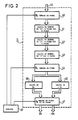
- the calculation circuit 11 of Sn and of -Sn is detailed in FIG. 2.
- the signals conveyed by the 8 channels are, first of all, entered into at least one fitness circuit 40.
- a first calculation circuit 41 then makes it possible to obtain the number N1 of "1" binaries present in a word of rank n, two paths by two paths, in a manner known to those skilled in the art. Indeed if we consider two channels V1 and V2, the most significant of this number is equal to V1.V2 and its least significant is V1 + V2. This number N1 is then calculated, using adder circuits 42 and 43, for 2 times 4 channels and finally for the set of 8 channels always for the same word of rank n. These circuits are followed by a fitness circuit 44.
- a fitness and phase 47 circuit then acts on these Sn and-Sn signals.
- the two sampler circuits 18 and 19 allow a reshaping and in phase of En of and z ' n .
- the circuit for inverting the digits of the word of rank n can be produced using "or exclusive" circuits, one of the inputs of which is connected to the output of the comparator circuit 22, the third sampler 33 then allowing a reset form of the 8 channels to which is joined a 9th channel on which the output signal of said comparator circuit 22 is sent.
- phase shift of H 4 compared to H 3 is explained by the delay of 1.7 periods at 140 Mb / s (12ns) introduced by circuits 40, 41, 42, 43.
- the delay of H s with respect to H 4 results from the propagation time introduced by the circuits 44 and 45 (or 46), which is around 1.1 periods (i.e. 7.5ns).
- H 2 is in synchronism with Hs taking into account the propagation times of the circuits included in the calculation loop (1 period).
- phase shift of Hi with respect to H 3 results from the propagation time introduced by circuits 30 and 32, which is of the order of 3.9 periods at 140 Mb / s, or approximately 27.5ns.
- the binary pulse trains can be transmitted on a serial channel, at a frequency equal to x times the base frequency and be demultiplexed at the input of the device in the form of x parallel information trains.
Description
La présente invention se rapporte à un dispositif de mise en oeuvre d'un code à faible disparité accumulée en transmission numérique à haut débit, par exemple à 8 fois 140 mégabits/seconde et à un procédé de codage utilisant un tel dispositif.The present invention relates to a device for implementing a low disparity code accumulated in high speed digital transmission, for example at 8 times 140 megabits / second and to a coding method using such a device.
Dans le domaine des transmissions numériques telles que ci-dessus définies, il est souhaitable que chaque train d'impulsions binaires, 0 ou 1, qui constitue un signal n'ait pas de composante continue et présente une faible densité d'énergie spectrale dans le domaine des basses-fréquences. En effet les têtes optiques d'émission et de réception utilisées présentent une coupure en basse-fréquence. De plus il est nécessaire de transmettre en basse-fréquence à la fois des informations de service et des informations de télésurveillance qui risquent alors de se brouiller entre elles.In the field of digital transmissions as defined above, it is desirable that each train of binary pulses, 0 or 1, which constitutes a signal has no DC component and has a low spectral energy density in the low frequency range. In fact, the transmission and reception optical heads used have a low-frequency cutoff. In addition, it is necessary to transmit at low frequency both service information and telemonitoring information which may then interfere with each other.
Pour réaliser cette propriété, il est connu, par exemple du document US-A-3.405.235, de découper le train numérique, se propageant en parallèle sur plusieurs voies, en mots transmis en parallèle auxquels on applique un code de bloc conçu pour que la disparité accumulée :
Le procédé de codage à disparité accumulée faible tel que décrit dans le document US-A-3.405.235 précité, est le suivant :
- - si Zn-1 et Sn sont de mêmes signes, le mot, de somme Sn, est inversé, c'est-à-dire que les "0" sont transformés en "1" et vice-versa,
- - si Σn-1 et Sn sont de signes contraires, le mot, de somme Sn, est transmis tel quel.
- - if Zn-1 and Sn are of the same signs, the word, of sum Sn, is inverted, that is to say that the "0" are transformed into "1" and vice versa,
- - if Σn-1 and Sn are of opposite signs, the word, of sum Sn, is transmitted as it is.
Les réalisations antérieures de ce code à faible disparité accumulée mettaient en oeuvre soit des mémoires programmables, inutilisables à l'heure actuelle à haut débit en raison de leurs temps d'accès trop élevés, soit un ou plusieurs additionneurs, dont la fréquence limite est trop faible et le temps de propagation trop élevé pour pouvoir être utilisés dans les mêmes conditions à un débit élevé, de l'ordre de 140 mégabits seconde par exemple.The previous embodiments of this low disparity accumulated code implemented either programmable memories, unusable at present at high speed because of their too long access times, or one or more adders, whose frequency limit is too low and the propagation time too long to be able to be used under the same conditions at a high speed, of the order of 140 megabits per second for example.
Pour pallier ces différents inconvénients, l'invention a pour objet l'utilisation de deux unités de calcul de En = En-1 + Sn et Σ'n = Sn-1 - Sn fonctionnant simultanément et en parallèle.To overcome these various drawbacks, the invention relates to the use of two calculation units of En = En- 1 + Sn and Σ'n = S n - 1 - Sn operating simultaneously and in parallel.
La présente invention présente à cet effet un dispositif de mise en oeuvre d'un code à faible disparité accumulée en transmission numérique, à haut débit, d'informations groupées sous la forme de mots binaires de x digits, un mot de rang n ayant une somme Sn égale à la demi-différence entre le nombre de "1" et nombre de "0" de ce mot, ledit dispositif comprenant un circuit de calcul de cette somme Sn, une unité de calcul de la disparité accumulée
un circuit de comparaison des signes de Σn-1 et de Sn, un circuit de codage de ce mot de rang n, un circuit délivrant des signaux d'horloge, caractérisé en ce que l'unité de calcul de la disparité accumulée comprend une première unité de calcul de la somme Σn = Σn-1 + Sn et une deuxième unité de calcul de la différence 2' n = En-1 - Sn disposée en parallèle, sur la première le circuit de comparaison de signes de Xn-1 et de Sn ayant une sortie reliée directement à une entrée de remise à zéro de la première unité de calcul, à une entrée de validation du circuit de codage, et à une entrée de ce même circuit de codage pour former en sortie un x+1 e digit de ce mot, et indirectement, à travers un inverseur, à une entrée de remise à zéro de la deuxième unité de calcul.The present invention therefore presents a device for implementing a low disparity code accumulated in digital transmission, at high speed, of information grouped in the form of binary words of x digits, a word of rank n having a sum Sn equal to the half-difference between the number of "1" and number of "0" of this word, said device comprising a circuit for calculating this sum Sn, a unit for calculating the accumulated disparity
a circuit for comparing the signs of Σn-1 and Sn, a circuit for coding this word of rank n, a circuit delivering clock signals, characterized in that the unit for calculating the accumulated disparity comprises a first unit for calculating the sum Σn = Σn-1 + Sn and a second unit for calculating the difference 2 'n = En-1 - Sn arranged in parallel, on the first the circuit for comparing the signs of Xn-1 and Sn having an output directly connected to a reset input of the first calculation unit, to a validation input of the coding circuit, and to an input of this same coding circuit to form an x + 1 th digit output of this word, and indirectly, through an inverter, to a reset input of the second calculation unit.
L'invention présente le grand avantage de permettre une transmission numérique à débit élevé, par exemple 8 fois 140 mégabits/seconde.The invention has the great advantage of allowing digital transmission at high speed, for example 8 times 140 megabits / second.
Plus particulièrement l'invention se rapporte à un dispositif caractérisé en ce que la transmission numérique se fait sur plusieurs voies en parallèle, un mot étant alors formé de l'ensemble des informations qui arrivent simultanément sur ces voies.More particularly the invention relates to a device characterized in that the digital transmission takes place over several channels in parallel, a word then being formed from all of the information which arrives simultaneously on these channels.
Les caractéristiques et avantages de l'invention ressortiront d'ailleurs de la description qui va suivre en références aux figures annexées sur lesquelles :
- - la figure 1 est une représentation schématique du dispositif de codage de l'invention,
- . - la figure 2 est une représentation schématique plus détaillée d'une partie du dispositif de l'invention.
- - la figure 3 est un diagramme représentant la phase relative des horloges par rapport à la phase des trains affluents.
- FIG. 1 is a schematic representation of the coding device of the invention,
- . - Figure 2 is a more detailed schematic representation of part of the device of the invention.
- - Figure 3 is a diagram showing the relative phase of the clocks with respect to the phase of the tributary trains.
Le dispositif de codage de l'invention comprend deux ensembles 8 et 9 disposés en parallèle : d'une part une boucle de calcul 8 de la disparité accumulée Σn et d'autre part un circuit de codage 9 des mots à transmettre.The coding device of the invention comprises two
En entrée arrivent un ensemble 10 de x voies parallèles qui attaquent ces deux ensembles 8 et 9.At the entrance comes a
Le premier ensemble 8 comporte un circuit de calcul 11 d'une somme Sn telle que 2 Sn = nombre de "1" binaires - nombre de "0" binaires d'un mot "de rang n" qui est formé de l'ensemble des informations qui entrent en parallèle dans ledit circuit 11.The
Ce circuit de calcul de Sn 11 permet de calculer également - Sn.This
Un premier et un second circuits additionneurs 12 et 13, dont deux premières séries d'entrées 14 et 15 reliées aux sorties Sn et -Sn du premier circuit 11 permettent de calculer respectivement Σn-1 + Sn et ln-1 - Sn ; la disparité accumulée En-1 étant telle que:
Un circuit de comparaison 22 des signes de En-1 et Sn a une première entrée 23 reliée à la sortie du circuit de calcul 11 de Sn correspondant au signe de Sn et une deuxième entrée 24 reliée à l'entrée d'un des deux circuits additionneurs 12 ou 13 qui correspond au signe de En-1 . Une sortie 25 de ce circuit de comparaison 22 est reliée directement à une entrée de remise à zéro du premier échantillonneur 18 et indirectement à travers un circuit inverseur 26 à une entrée de remise à zéro du deuxième échantillonneur 19.A
Le deuxième ensemble 9 comprend un circuit retardateur 30 qui reçoit les x voies 10 d'entrée en parallèle avec le circuit de calcul de Sn 11.The second set 9 comprises a
Les x sorties 31 de ce circuit retardateur 30 sont reliées à un circuit de codage 32 des informations véhiculées sur les x voies, qui permet l'inversion ou non de celles-ci.The
Un troisième circuit d'échantillonnage 33 est relié aux sorties 34 de ce circuit 32.A
L'entrée de validation 35 de ce circuit de codage 32 est reliée à la sortie 25 du circuit comparateur 22 des signes de Σn-1 et de Sn ; cette sortie 25 étant également reliée au troisième échantillonneur 33 pour former une x + 1 des voies de sortie 36 de celui-ci.The
Un circuit horloge 37 délivre différents signaux horloge Hi, de même fréquence mais déphasés les uns par rapport aux autres, au circuit de calcul 11 de Sn et de - Sn et aux différents échantillonneurs 18, 19 et 33, l'entrée H de la figure 1 correspondant aux entrées Hs, H4 et Hs de la figure 2.A
En fonctionnement les informations arrivent en entrée sous la forme de trains parallèles d'impulsions binaires ; un mot étant formé de l'ensemble des informations qui attaquent simultanément le dispositif de l'invention. Celui-ci permet après obtention de Sn et- Sn, de calculer simultanément à l'aide des deux circuits additionneurs 12 et 13 qui présentent un temps de propagation faible ; Σn = Σn-1 + Sn et Σ'n = Σn-1 - Sn pendant que se calcule l'information de comparaison des signes de Σn-1 et de Sn.In operation, the information arrives at the input in the form of parallel trains of binary pulses; a word being formed from all of the information which simultaneously attacks the device of the invention. This makes it possible, after obtaining Sn and Sn, to calculate simultaneously using the two
Le signal de sortie du circuit de comparaison permet lorsque les signes de Σn-1 et de Sn sont différents, la remise à zéro du deuxième échantillonneur 19, et lorsqu'ils sont égaux, la remise à zéro du premier échantillonneur 18 et l'inversion 32 de tous les digits du mot de rang n, le (x + 1)e digit introduit en sortie du troisième échantillonneur 33; qui est alors du niveau "1" permettant de savoir qu'une inversion du mot de rang n a eu lieu.The output signal of the comparison circuit allows when the signs of Σ n-1 and Sn are different, the resetting of the
Le circuit retardateur 30 permet la prise en compte et la comparaison des signes de ln-1 et de Sn avec envoi éventuel d'un signal de validation de l'inversion de tous les digits du mot de rang n en entrée 35 du circuit 32 avant que ce mot de rang n n'arrive en entrée 31 du même circuit 32.The
Le dispositif de l'invention permet donc coder chaque mot du train d'information de telle sorte que la disparité accumulée in reste faible.The device of the invention therefore makes it possible to code each word of the information train so that the disparity accumulated in remains low.
Dans un exemple particulier de réalisation on considère le dispositif de l'invention muni de 8 voies d'entrée.In a particular embodiment, we consider the device of the invention provided with 8 input channels.
Le circuit de calcul 11 de Sn et de -Sn est détaillé à la figure 2.The
Les signaux véhiculés par les 8 voies sont, tout d'abord, entrés dans au moins un circuit de remise en forme 40.The signals conveyed by the 8 channels are, first of all, entered into at least one
Un premier circuit de calcul 41 permet ensuite d'obtenir le nombre N1 de "1" binaires présents dans un mot de rang n, deux voies par deux voies, de manière connue de l'homme de l'art. En effet si l'on considère deux voies V1 et V2, le poids fort de ce nombre est égal à V1.V2 et son poids faible à V1 + V2. Ce nombre N1 est ensuite calculé, à l'aide de circuits additionneurs 42 et 43, pour 2 fois 4 voies et enfin pour l'ensemble de 8 voies toujours pour un même mot de rang n. Ces circuits sont suivis d'un circuit de remise en forme 44.A first calculation circuit 41 then makes it possible to obtain the number N1 of "1" binaries present in a word of rank n, two paths by two paths, in a manner known to those skilled in the art. Indeed if we consider two channels V1 and V2, the most significant of this number is equal to V1.V2 and its least significant is V1 + V2. This number N1 is then calculated, using
Si l'on écrit les tables de vérité de Sn et de N1, pour 8 voies, l'on trouve, de manière connue de l'homme de l'art que Sn = N1-4 et donc que - Sn = 4 - N1 = N1 + 5, en valeur complétée à 2. Les circuits 45 et 46 connus de l'homme de l'art permettent d'obtenir ces valeurs Sn et-Sn.If we write the truth tables of Sn and N1, for 8 channels, we find, in a manner known to those skilled in the art that Sn = N1-4 and therefore that - Sn = 4 - N1 = N1 + 5, in value completed with 2. The
Un circuit de remise en forme et en phase 47 agit alors sur ces signaux Sn et-Sn.A fitness and
Après calcul de Σn = Σn-1 + Sn et Σ'n = ln-1 - Sn, les deux circuits échantillonneurs 18 et 19 permettent une remise en forme et en phase de En de et z'n.After calculating Σ n = Σ n-1 + Sn and Σ'n = ln-1 - Sn, the two
La sélection de la valeur de Σn en Σ'n s'effectue en fonction de la comparaison des signes de En-1 et de Sn.The selection of the value of Σ n in Σ ' n is carried out as a function of the comparison of the signs of En- 1 and Sn.
La remise à zéro de l'une de ces deux valeurs permet, grâce à des "ou câblé" par exemple, d'obtenir la valeur de la disparité accumulée En qui sera alors utilisé pour le calcul de Σn+1 = En ± Sn.The reset to zero of one of these two values allows, thanks to "or wired" for example, to obtain the value of the accumulated disparity En which will then be used for the calculation of Σ n + 1 = En ± Sn .
Le circuit d'inversion des digits du mot de rang n peut être réalisé à l'aide de circuits "ou exclusif" dont l'une des entrées est reliée à la sortie du circuit comparateur 22, le troisième échantillonneur 33 permettant alors une remise en forme des 8 voies auxquelles est jointe une 9è voie sur laquelle est envoyée le signal de sortie dudit circuit comparateur 22.The circuit for inverting the digits of the word of rank n can be produced using "or exclusive" circuits, one of the inputs of which is connected to the output of the
Le diagramme des temps représenté à la figure 3 correspond à un exemple de réalisation du dispositif de codage de l'invention en technologie ECL 100.000, pour un débit des trains affluents en 10 (TA) de 140 Mb/s (période = 7,2ns).The time diagram represented in FIG. 3 corresponds to an exemplary embodiment of the coding device of the invention in ECL 100,000 technology, for a flow of the tributary trains in 10 (TA) of 140 Mb / s (period = 7.2 ns ).
Le déphasage de H4 par rapport à H3 s'explique par le retard de 1,7 période à 140 Mb/s (12ns) introduit par les circuits 40, 41, 42, 43.The phase shift of H 4 compared to H 3 is explained by the delay of 1.7 periods at 140 Mb / s (12ns) introduced by
Le retard de Hs par rapport à H4 résulte du temps de propagation introduit par les circuits 44 et 45 (ou 46), qui est de l'ordre de 1,1 période (soit 7,5ns).The delay of H s with respect to H 4 results from the propagation time introduced by the
H2 se trouve en synchronisme avec Hs compte tenu des temps de propagation des circuits compris dans la boucle de calcul (1 période).H 2 is in synchronism with Hs taking into account the propagation times of the circuits included in the calculation loop (1 period).
Le déphasage de Hi par rapport à H3 résulte du temps de propagation introduit par les circuits 30 et 32, qui est de l'ordre de 3,9 périodes à 140 Mb/s, soit 27,5ns environ.The phase shift of Hi with respect to H 3 results from the propagation time introduced by
Les trains d'impulsions binaires peuvent être transmis sur une voie en série, à une fréquence égale à x fois la fréquence de base et être démulti- plexés en entrée du dispositif sous la forme de x trains d'informations parallèles.The binary pulse trains can be transmitted on a serial channel, at a frequency equal to x times the base frequency and be demultiplexed at the input of the device in the form of x parallel information trains.
Claims (8)

Applications Claiming Priority (2)
| Application Number | Priority Date | Filing Date | Title |
|---|---|---|---|
| FR8516372A FR2589653B1 (en) | 1985-11-05 | 1985-11-05 | DEVICE FOR IMPLEMENTING AN ACCUMULATED LOW DISPARITY CODE IN HIGH-SPEED DIGITAL TRANSMISSION AND CODING METHOD USING SUCH A DEVICE |
| FR8516372 | 1985-11-05 |
Publications (2)
| Publication Number | Publication Date |
|---|---|
| EP0228528A1 EP0228528A1 (en) | 1987-07-15 |
| EP0228528B1 true EP0228528B1 (en) | 1990-07-11 |
Family
ID=9324510
Family Applications (1)
| Application Number | Title | Priority Date | Filing Date |
|---|---|---|---|
| EP86115074A Expired - Lifetime EP0228528B1 (en) | 1985-11-05 | 1986-10-30 | Apparatus for implementing a code with a small digital sum variation in a fast digital transmission, and coding method using such an apparatus |
Country Status (4)
| Country | Link |
|---|---|
| US (1) | US4731797A (en) |
| EP (1) | EP0228528B1 (en) |
| DE (1) | DE3672588D1 (en) |
| FR (1) | FR2589653B1 (en) |
Families Citing this family (12)
| Publication number | Priority date | Publication date | Assignee | Title |
|---|---|---|---|---|
| JPH0244583A (en) * | 1988-08-05 | 1990-02-14 | Toshiba Corp | Data transmission equipment |
| US5341134A (en) * | 1992-12-30 | 1994-08-23 | Datatape Incorporated | Simple coding scheme for DC free channel codes of form M/N, where M=N-1 and M and N are positive integers |
| US5450443A (en) * | 1993-09-01 | 1995-09-12 | International Business Machines Corporation | Method and apparatus for constructing asymptotically optimal second order DC-free channel codes |
| US5644601A (en) | 1994-10-31 | 1997-07-01 | Symbol Technologies, Inc. | Method and apparatus for bias suppression in a VCO based FM transmission system |
| US5691931A (en) * | 1995-06-07 | 1997-11-25 | Hitachi America, Ltd. | Low power adder for accumulation |
| US5898394A (en) * | 1996-07-31 | 1999-04-27 | Matsushita Electric Industrial Co., Ltd. | Code conversion method and apparatus, code recording medium, code recording apparatus and code reproducing apparatus |
| USRE39771E1 (en) * | 1996-07-31 | 2007-08-14 | Matsushita Electric Industrial Co., Ltd. | Code conversion method and apparatus, code recording medium, code recording apparatus and code reproducing apparatus |
| GB2334188A (en) * | 1998-02-05 | 1999-08-11 | Motorola Gmbh | Direct current (dc) balancing in an ac coupled system |
| KR100296787B1 (en) | 1998-11-06 | 2001-10-26 | 구본준, 론 위라하디락사 | Preventing Circuit of Rush Current for Liquid Crystal Dispaly |
| KR100313243B1 (en) | 1998-12-31 | 2002-06-20 | 구본준, 론 위라하디락사 | Device for transmitting Data and Method thereof |
| KR100669095B1 (en) | 1999-12-28 | 2007-01-16 | 엘지.필립스 엘시디 주식회사 | Data Transmitting/Receiving Method and Apparatus, and Liquid Crystal Display and Driving Method thereof |
| DE10033130A1 (en) * | 2000-07-07 | 2002-01-31 | Infineon Technologies Ag | Method and device for digitally coding binary data with a specific transmission signal spectrum |
Family Cites Families (6)
| Publication number | Priority date | Publication date | Assignee | Title |
|---|---|---|---|---|
| NL136990C (en) * | 1968-07-12 | |||
| GB1540617A (en) * | 1968-12-13 | 1979-02-14 | Post Office | Transformation of binary coded signals into a form having lower disparity |
| US4027335A (en) * | 1976-03-19 | 1977-05-31 | Ampex Corporation | DC free encoding for data transmission system |
| JPS5665314A (en) * | 1979-11-02 | 1981-06-03 | Sony Corp | Encoder for binary signal |
| JPH0683271B2 (en) * | 1983-10-27 | 1994-10-19 | ソニー株式会社 | Information conversion method |
| NL8402444A (en) * | 1984-01-20 | 1986-03-03 | Philips Nv | METHOD FOR TRANSFERRING INFORMATION, CODER FOR APPLICATION IN THE METHOD AND DECODER FOR APPLICATION IN THE METHOD |
-
1985
- 1985-11-05 FR FR8516372A patent/FR2589653B1/en not_active Expired - Fee Related
-
1986
- 1986-10-30 EP EP86115074A patent/EP0228528B1/en not_active Expired - Lifetime
- 1986-10-30 DE DE8686115074T patent/DE3672588D1/en not_active Expired - Fee Related
- 1986-11-05 US US06/927,198 patent/US4731797A/en not_active Expired - Fee Related
Also Published As
| Publication number | Publication date |
|---|---|
| DE3672588D1 (en) | 1990-08-16 |
| FR2589653A1 (en) | 1987-05-07 |
| US4731797A (en) | 1988-03-15 |
| FR2589653B1 (en) | 1990-03-23 |
| EP0228528A1 (en) | 1987-07-15 |
Similar Documents
| Publication | Publication Date | Title |
|---|---|---|
| EP0228528B1 (en) | Apparatus for implementing a code with a small digital sum variation in a fast digital transmission, and coding method using such an apparatus | |
| EP0419337B1 (en) | Digital signal encoding method, encoder and decoder for carrying out the method, regeneration method and regenerator therefore | |
| FR2463996A1 (en) | DIGITAL SIGNAL TRANSMISSION SYSTEM | |
| EP0162442B1 (en) | Synchronous data transmission method and device for carrying it out | |
| EP0246701A1 (en) | DPCM coder and associated decoder | |
| EP0112953A1 (en) | Method of dynamic assignment of speeds in a multiplex transmission system | |
| EP0026699B1 (en) | Method and device for coding digital data, device for decoding digital data and a transmission system comprising such a device | |
| EP0018242B1 (en) | Method and device for stochastic demodulation of phase-shift keyed signals working in time division on several channels | |
| FR2531588A1 (en) | DIGITAL MULTIPLEX SYSTEM OF THE FOURTH ORDER FOR TRANSMITTING A NUMBER OF DIGITAL SIGNALS AT A NOMINAL BIT RATE OF 44.736 KBITS / SEC. | |
| CH640678A5 (en) | METHOD AND INSTALLATION FOR THE SIMULTANEOUS TRANSMISSION OF A LOW FREQUENCY WAVE AND A MIC DIGITAL SIGNAL. | |
| CH661624A5 (en) | METHOD AND APPARATUS FOR CONVERTING DIGITAL DATA. | |
| FR2467516A1 (en) | CIRCUIT ARRANGEMENT CAPABLE OF RECOGNIZING THE ALIGNMENT SPEECH APPLYING PARTICULARLY TO THE RECEPTOR SECTION OF A DIGITAL SIGNAL MULTIPLEXER | |
| EP0130899A2 (en) | Programmable series/parallel converter circuit for a digital signal, and its use in a receiver for digital video signals | |
| FR2493646A1 (en) | Synchroniser for analogue modulation transmitted data - operates on digital information samples rectified analogue signals at rate varied according to summation of various sample group amplitudes | |
| EP0227521B1 (en) | Method for the cmi coding of digital information arranged in frames, apparatus for carrying it out and its use in consumer information for very fast digital networks | |
| EP0396461B1 (en) | Device for synchronising a pseudo-binary signal with a phase-hopped regenerated clock signal | |
| FR2643524A1 (en) | METHOD AND DEVICE FOR BIT SYNCHRONIZATION IN A DIGITAL DATA TRANSMISSION RECEIVER | |
| EP0165122A1 (en) | Synchronisation circuit in a multiplexer of plesiochronic digital signals | |
| EP0229738B1 (en) | Method and device for the regeneration of the integrity of the binary throughput in a pleisiochronous network | |
| FR2501937A1 (en) | DEVICE FOR SWITCHING DATA TRANSMISSION PATHWAYS | |
| EP0196979A1 (en) | Method and device for inserting a digital signal into a higher rate channel | |
| EP0288353B1 (en) | Method for switching asyschronous digital signals, and device for carrying out this method | |
| FR2643481A1 (en) | METHOD AND DEVICE FOR TRANSMITTING INFORMATION BETWEEN STATIONS IN A COMMUNICATION NETWORK, IN PARTICULAR FOR A MOTOR VEHICLE | |
| FR2488089A1 (en) | INFORMATION TRANSCODING METHOD AND TRANSMISSION SYSTEM USING SUCH A METHOD | |
| EP0184953B1 (en) | Method and device for digital information transmission using differential frequency shift keying |
Legal Events
| Date | Code | Title | Description |
|---|---|---|---|
| PUAI | Public reference made under article 153(3) epc to a published international application that has entered the european phase |
Free format text: ORIGINAL CODE: 0009012 |
|
| AK | Designated contracting states |
Kind code of ref document: A1 Designated state(s): BE DE FR GB IT LU NL SE |
|
| 17P | Request for examination filed |
Effective date: 19880111 |
|
| 17Q | First examination report despatched |
Effective date: 19890823 |
|
| RAP1 | Party data changed (applicant data changed or rights of an application transferred) |
Owner name: ALCATEL CIT |
|
| GRAA | (expected) grant |
Free format text: ORIGINAL CODE: 0009210 |
|
| AK | Designated contracting states |
Kind code of ref document: B1 Designated state(s): BE DE FR GB IT LU NL SE |
|
| REF | Corresponds to: |
Ref document number: 3672588 Country of ref document: DE Date of ref document: 19900816 |
|
| GBT | Gb: translation of ep patent filed (gb section 77(6)(a)/1977) | ||
| ITF | It: translation for a ep patent filed |
Owner name: JACOBACCI & PERANI S.P.A. |
|
| PLBE | No opposition filed within time limit |
Free format text: ORIGINAL CODE: 0009261 |
|
| STAA | Information on the status of an ep patent application or granted ep patent |
Free format text: STATUS: NO OPPOSITION FILED WITHIN TIME LIMIT |
|
| 26N | No opposition filed | ||
| PGFP | Annual fee paid to national office [announced via postgrant information from national office to epo] |
Ref country code: LU Payment date: 19911015 Year of fee payment: 6 |
|
| EPTA | Lu: last paid annual fee | ||
| PG25 | Lapsed in a contracting state [announced via postgrant information from national office to epo] |
Ref country code: LU Free format text: LAPSE BECAUSE OF NON-PAYMENT OF DUE FEES Effective date: 19921030 |
|
| PGFP | Annual fee paid to national office [announced via postgrant information from national office to epo] |
Ref country code: GB Payment date: 19930825 Year of fee payment: 8 |
|
| PGFP | Annual fee paid to national office [announced via postgrant information from national office to epo] |
Ref country code: SE Payment date: 19930922 Year of fee payment: 8 Ref country code: DE Payment date: 19930922 Year of fee payment: 8 |
|
| PGFP | Annual fee paid to national office [announced via postgrant information from national office to epo] |
Ref country code: FR Payment date: 19930930 Year of fee payment: 8 |
|
| PGFP | Annual fee paid to national office [announced via postgrant information from national office to epo] |
Ref country code: BE Payment date: 19931022 Year of fee payment: 8 |
|
| ITTA | It: last paid annual fee | ||
| PGFP | Annual fee paid to national office [announced via postgrant information from national office to epo] |
Ref country code: NL Payment date: 19931031 Year of fee payment: 8 |
|
| PG25 | Lapsed in a contracting state [announced via postgrant information from national office to epo] |
Ref country code: GB Effective date: 19941030 |
|
| PG25 | Lapsed in a contracting state [announced via postgrant information from national office to epo] |
Ref country code: SE Effective date: 19941031 Ref country code: BE Effective date: 19941031 |
|
| EAL | Se: european patent in force in sweden |
Ref document number: 86115074.6 |
|
| BERE | Be: lapsed |
Owner name: ALCATEL CIT Effective date: 19941031 |
|
| PG25 | Lapsed in a contracting state [announced via postgrant information from national office to epo] |
Ref country code: NL Effective date: 19950501 |
|
| NLV4 | Nl: lapsed or anulled due to non-payment of the annual fee | ||
| GBPC | Gb: european patent ceased through non-payment of renewal fee |
Effective date: 19941030 |
|
| PG25 | Lapsed in a contracting state [announced via postgrant information from national office to epo] |
Ref country code: FR Effective date: 19950630 |
|
| PG25 | Lapsed in a contracting state [announced via postgrant information from national office to epo] |
Ref country code: DE Effective date: 19950701 |
|
| EUG | Se: european patent has lapsed |
Ref document number: 86115074.6 |
|
| REG | Reference to a national code |
Ref country code: FR Ref legal event code: ST |
|
| PG25 | Lapsed in a contracting state [announced via postgrant information from national office to epo] |
Ref country code: IT Free format text: LAPSE BECAUSE OF NON-PAYMENT OF DUE FEES;WARNING: LAPSES OF ITALIAN PATENTS WITH EFFECTIVE DATE BEFORE 2007 MAY HAVE OCCURRED AT ANY TIME BEFORE 2007. THE CORRECT EFFECTIVE DATE MAY BE DIFFERENT FROM THE ONE RECORDED. Effective date: 20051030 |