EP0227464A2 - High density read-only memory - Google Patents
High density read-only memory Download PDFInfo
- Publication number
- EP0227464A2 EP0227464A2 EP86310023A EP86310023A EP0227464A2 EP 0227464 A2 EP0227464 A2 EP 0227464A2 EP 86310023 A EP86310023 A EP 86310023A EP 86310023 A EP86310023 A EP 86310023A EP 0227464 A2 EP0227464 A2 EP 0227464A2
- Authority
- EP
- European Patent Office
- Prior art keywords
- lines
- row
- select
- address
- line
- Prior art date
- Legal status (The legal status is an assumption and is not a legal conclusion. Google has not performed a legal analysis and makes no representation as to the accuracy of the status listed.)
- Granted
Links
Images

Classifications
-
- G—PHYSICS
- G11—INFORMATION STORAGE
- G11C—STATIC STORES
- G11C17/00—Read-only memories programmable only once; Semi-permanent stores, e.g. manually-replaceable information cards
- G11C17/08—Read-only memories programmable only once; Semi-permanent stores, e.g. manually-replaceable information cards using semiconductor devices, e.g. bipolar elements
- G11C17/10—Read-only memories programmable only once; Semi-permanent stores, e.g. manually-replaceable information cards using semiconductor devices, e.g. bipolar elements in which contents are determined during manufacturing by a predetermined arrangement of coupling elements, e.g. mask-programmable ROM
- G11C17/12—Read-only memories programmable only once; Semi-permanent stores, e.g. manually-replaceable information cards using semiconductor devices, e.g. bipolar elements in which contents are determined during manufacturing by a predetermined arrangement of coupling elements, e.g. mask-programmable ROM using field-effect devices
- G11C17/126—Virtual ground arrays
Definitions
- This invention relates generally to integrated circuit memories, and more particularly, to read-only integrated circuit memories (ROMS).
- ROMS read-only integrated circuit memories
- ROM read-only memory
- X-ROM X-ROM described in an article entitled "A 100ns 150mW 64K Bit ROM" by D.R. Wilson and P.R. Schroeder, ISSCC DIGEST OF TECHNICAL PAPERS, pp. 152-153, 273, Feb. 1978.
- This paper discloses a memory having a first set of horizontally extending row electrical conductors or row lines, and two sets of vertically extending electrical conductors, one set called data lines and the other set called column lines.
- the data lines and column lines are physically arranged in an alternating pattern.
- the column lines are themselves alternately interconnected to form two groups of column lines.
- the bit lines carry data from the memory cells to sense amplifiers.
- Memory cells are arranged in an array NxM in regions bounded by the two sets of column lines and the set of row lines. Each memory cell is coupled to an adjacent column line, an adjacent bit line, and an adjacent row line. Memory cells are selected by enabling one column line and one row line. Therefore, each row address conductor has M memory cells coupled thereto and each column line has 2N memory cells coupled thereto.
- one of the row lines is enabled and one of the two groups of column lines is enabled. This causes those memory cells coupled to the enabled row line and to the enabled column lines to transfer their stored information to their respective bit lines.
- Each column line is heavily loaded capacitively because of the 2N memory cells coupling to it.
- This capacitive loading reduces access time of the memory due to a delay necessary to insure complete charging of the heavily loaded column lines.
- large, high power column line drivers are required. Therefore, with each access of the memory, one set of the column lines and associated drivers are active, causing high power dissipation and high electrical noise generation.
- these column line drivers and associated column line decoders are located apart from row line drivers and associated row line decoders. By using separate row line and column line decoders with large column line drivers, less area is available to the memory for memory cells.
- Another object of this invention is to provide a decoder which uses common circuitry to drive the column and row drivers.
- each select line has half the capacitive loading a column line in the prior art has.
- a row line is enabled and only those select lines corresponding to the enabled row line (typically one or two) are enabled instead of half of the column lines as in the prior art. Therefore, with each select line being lightly loaded and with only one or two of corresponding select lines enabled, less electrical noise is generated and less power is dissipated during a read of the memory compared to the prior art.
- the smaller loading on the select lines allows smaller, less powerful drivers to drive these select lines compared to the column line drivers needed in the prior art.
- decoders for the select lines can share decoding logic with the row decoders.
- an address and select line decoder uses multiple stages of decoders to decode an input address.
- Decoding of the input address has several common stages of decoding, allowing an efficient scheme to enable one row line and have only those select lines enabled that correspond to that enabled row line. By enabling only those select lines that correspond to an enabled row line, power dissipation, electrical noise generation and access time of the memory is reduced. Additionally, common decoder circuitry allows more chip area available for memory cells.
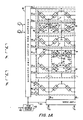
- a semiconductor integrated circuit memory (ROM) 10 is shown to include: an array 12 of memory cells 14, arranged in pairs 17.
- the memory cells 14 are arranged in a matrix of 2 m rows 71 and n columns (not numbered), as shown, storing 2 m by n bit digital words, where m is the number of bits used to address the ROM 10.
- Corresponding with each row 71 are a pair of 2 m-1 select lines SL0 ⁇ -SL (2 m -1) ⁇ .
- One of the pair of corresponding select lines SL0 ⁇ -SL (2 m-1 ) ⁇ is connected to a first one of the memory cells 14 in each pair 17 and the second one of the pair of corresponding select lines SL0 ⁇ -SL (2 m -1) ⁇ is connected to the other one of the memory cells 14 in the pair 17. It is next noted that a pair of adjacent row lines RL0-RL (2 m-1 ) is disposed between successive select lines SL0 ⁇ -SL (2 m-1 ) ⁇ and each row line RL0-RL (2 m-1 ) couples to each memory cell 14 in corresponding rows 71.
- the memory 10 also includes: an address and select line decoder 16; a sense amplifier section 18; and a ROM enable circuit 62.
- decoder 16 enables, or addresses, one of 2 m row conductors (i.e., row lines RL0-RL (2 m -1) , as shown, selectively in accordance with address signals on lines A0-A m-1 . More particularly, decoder 16 drives all but one of the row lines RL0-RL (2 m -1) “low” (to ground) while driving the enabled or addressed row line RL0-RL (2 m -1) “high” (+V DD ).
- the address and select line decoder 16 enables, or addresses, a selected two of the select SL0 ⁇ -SL (2 m -1) ⁇ , corresponding to the enabled row line RL0-RL (2 m -1) during a read of the ROM.
- Column conductors, or bit lines BL0-BL (n-1) carry the binary data accessed in addressed memory cells 14 to the sense amplifier section 18 to thereby read from the memory cell array 12 the n-bits of the addressed one of the 2 m+1 n-bit digital words stored in such ROM 10; such digital words having been masked programmed into the ROM 10 during its fabrication as an integrated circuit.
- the sense amplifiers in the sense amplifier section 18 are of a conventional design, each one thereof being coupled to a corresponding one of the bit lines BL0-BL (n-1) to produce at the output of such sense amplifier section 18 an n-bit digital word O0-O (n-1) .
- the sense amplifier section 18 and address and select line decoder 16 are controlled by the ROM enable circuitry 62 by the enable signal on line 64.
- An external input chip enable signal fed to input 60 controls ROM enable circuitry 62 by enabling ROM enable circuitry 62 when a ROM read cycle is requested (input 60 is "high”) and disabling it when in the standby mode (input 60 is "low”).
- each memory cell 14 in that pair 17 has an output terminal 32, enable terminal 30 and an address terminal 31 disposed between the enable terminal 30 and the output terminal 32.
- the output terminals 32 in each memory cell pair 17 are coupled to a common output terminal 24, which are in turn coupled to a corresponding bit line BL0-BL (2 n-1 ) .
- the address terminals 31 of all the memory cells 14 in each memory cell row 71 are coupled to a corresponding one of the row lines RL0-RL (2 m -1) .
- the select lines SL0 ⁇ -SL (2 m -1) ⁇ are disposed adjacent to alternating memory cell rows 71.
- the enable terminal 30 of a first one of the memory cells 14 in each memory cell pair 17 couples to a first one of the adjacent select lines SL0 ⁇ -SL (2 m -1) ⁇ and the enable terminal 30 of the second one of the memory cells 14 of the pair 17 couples to a different one of the adjacent select lines SL0 ⁇ -SL (2 m -1) ⁇ . Because each memory cell 14 of each memory cell pair 17 is coupled to a different one of the select lines SL0 ⁇ -SL (2 m-1 ) , when the corresponding row line RL0-RL (2 m-1 ) is enabled, the binary data stored in one of the memory cells 14 is passed to the common output terminal 24. Therefore, two memory cells 14 coupled to a common output terminal 24 cannot be enabled simultaneously.
- each memory cell 14 (FIGS. 1A, 1B) is an n-channel enhancement mode metal oxide semiconductor (MOS) field effect transistor (FET).
- MOS metal oxide semiconductor
- the output terminal 32 couples to the drain D
- the enable terminal 30 couples to the source S
- the address terminal 31 couples to the gate G of the FET.
- Each one of the cells 14 (FIGS. 1A, 1B) is programmed to have transistor action (to store a logic 0), as shown in FIG. 5A, or is programmed not to have transistor action (to store a logic 1) as shown in FIG. 5B.
- Transistor action occurs where signals on the address terminal 31 can control the conductivity between the drain D and the source S (FIG. 5A).
- Transistor action is inhibited where signals on the address terminal 31 cannot control the conductivity (FIG. 5B).
- transistor action is inhibited, a high impedance state exists between the source S and drain D.
- cell 14a is enabled, a low impedance state exists between the drain D and the source S.
- the ROM enable circuitry 62 controls the ROM 10 in a pre-charge state by placing a disable signal on line 64.
- address and select line decoder 16 is disabled so that all the row lines RL0-RL (2 m -1) are "low” (ground) and all the select lines SL0 ⁇ -SL (2 m -1) ⁇ are "high” (+V DD ).
- the disable signal on line 64 disables the sense amplifiers in the sense amplifier section 18 to pre-charge the bit lines BL0-BL (n-1) to +V DD .
- the ROM enable circuit 62 sends an enable signal on line 64, releasing the address and select line decoder 16 and the sense amplifiers in sense amplifier section 18 to access the desired memory cells 14.
- Operation of the ROM 10 during a read cycle while referring specifically, by way of example, to enable signals on row line RL1, select lines SL 0,1 and SL 2,3 , and an exemplary pair of memory cells 17a connected to bit line BL1, it is first noted that an enable signal on row line RL1 (a "high”) and select line SL 2,3 (a “low”) places the memory cell 14a′′′ into a conduction condition (having been programmed with transistor action), to discharge the stored charge over bit line BL1 from +V DD toward ground.
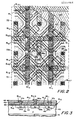
- FIG. 3 is a cross-sectional view along the 3-3 line in FIG. 2. It is additionally noted that each one of the memory cells 14 are formed in different regions of the semiconductor body used to fabricate the ROM 10 as an integrated circuit. During fabrication of the ROM 10 as an integrated circuit, those memory cells which are to store a logic 0 data bit have formed in that element an FET having transistor action, designated here as 14a (FIG. 5A). A memory cell 14 that stores a logical 1 by having its transistor action is designated as 14b (FIG. 5B).
- N+type conductivity regions 33a and 34a, 34c, forming the source S and drain D of cells 14a, 14b are diffused into a grounded p-type conductivity ground well 40.
- This well 40 is electrically coupled to ground through a ground bus (not shown).
- This well 40 is disposed in an n-type conductivity silicon substrate 41.
- the row lines RL0-RL (2 m -1) consist of doped polycrystalline silicon (polysilicon), with portions thereof providing gate electrodes G (FIGS. 5A, 5B). Further, as described above, the gate electrode G (FIG.
- memory element 14a is disposed over a thin silicon dioxide insulating layer 42 in etched area 50 (FIG. 3) of silicon dioxide on the portions of the surface of the well 40 between the regions 33a and 34a to provide an n-channel enhancement mode FET.
- a thick portion of silicon dioxide insulating layer 42 is formed between the regions 33a, 34c to destroy any gate channel between such regions 33a, 34c and thus inhibit transistor action between regions 33a, 34c. It is here noted that while the use of a thick oxide layer between the source and drain regions to prevent transistor action has been described, other conventional techniques can be used to prevent such transistor action, such as active area removal or implantation into the channel region to raise the transistor threshold for conducting current.
- the bit lines BL0-BL (n-1) are formed by a first level of metallization insulated from the polysilicon row lines RL0-RL (2 m -1) by oxide layer 43, and are arranged perpendicularly to the row lines RL0-RL (2 m -1) .
- the select lines SL0 ⁇ -SL (2 m -1) ⁇ are formed by a second level of metallization insulated from the bit lines BL0-BL (n-1) by oxide layer 44, and are arranged to parallel the row lines RL0-RL (2 m -1) .
- These select lines SL0 ⁇ -SL (2 m-1 ) ⁇ are coupled to corresponding n+type conductivity regions 33 via contacts 36, such regions being diffused within well 40.
- the second level of metallization first couples to a first level of metallization which, in turn, couples to the n+ type conductivity region instead of directly going from a second level of metallization to the n+ type conductivity region as shown.
- first level of metallization which, in turn, couples to the n+ type conductivity region instead of directly going from a second level of metallization to the n+ type conductivity region as shown.
- second level metal couples to a first level of metallization which, in turn, couples to the n+ type conductivity region instead of directly going from a second level of metallization to the n+ type conductivity region as shown.
- the bit lines BL0-BL (n-1) are coupled thereto via contacts 37, such regions being diffused within well 40.
- the select lines SL0 ⁇ , SL (2 m -1) ⁇ are arranged in rows such that they cross the semiconductor bulk comprising the ROM array over where the bit lines BL0-BL (n-1) couple to the n+ region contacts 37.
- the columns of bit lines BL0-BL (n-1) and the rows of select lines SL0 ⁇ -SL (2 m -1) ⁇ form rows and columns of regions 70, each region 70 having four memory cells 14 (FIGS. 1A, 1B). Rows and columns of these regions 70 form rows and columns of common enable terminals 36.
- the address terminals 31 (FIGS.
- a row 72 of regions 70 with common enable terminals 36 has first alternating ones of the common enable terminals coupling to an adjacent select line SL0 ⁇ -SL (2 m -1) ⁇ and second alternating ones of the common enable terminals 36 coupling to a different, adjacent select line SL0 ⁇ -SL (2 m -1) ⁇ .
- a n+ region 33a in the center of region 70a forms a common source S (FIGS.
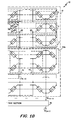
- a conventional decoder 100 selects one of the outputs S0,1-S (2 m -2) , (2 m -1) in response to the address line inputs A1-A m-1 . More specifically, the conventional decoder 100 contains two one-of-N decoders 110, 111, each of which respond to separate sets of address inputs, here one-of-N decoder 110 responds to address Aj-A m-2 and one-of-N decoder 111 responds to address A1-A j-1 .
- the outputs of the one-of-N decoders (112 for decoder 110 and 113 for decoder 111) are normally "high” (i.e., unselected outputs from decoders 110 and 111 are “high") and the selected one of each of the outputs 112, 113 is "low”.
- the NOR array 115 logically ANDs (negative logic) the outputs 112, 113 to produce one "high” output S0,1-S (2 m -2), (2 m -1) , while remaining S0,1-S (2 m -2), (2 m -1) are low.
- the outputs S0,1-S (2 m -2), (2 m -1) of the conventional decoder 100 corresponds to a pair of row lines RL0-RL (2 m -1) (i.e., S0,1 to RL0 and RL1, S2,3 to RL2 and RL3, etc.). Selection of which one of the row lines RL0-RL (2 m -1) corresponding to the enabled one of the outputs S0,1-S (2 m -2), (2 m -1) , occurs in the decoder array 120, in response to the select input S to the decoder array 120.
- the input S is coupled to the address line input A0.
- decoder 100 output S0,1 is “high” and A0 is “low”
- decoder 120a having its select input S “low”
- A0 is “high”
- RL1 would be enabled.
- one of the row lines RL0-RL (2 m -1) is "high” corresponding to the state of the A0 address input and the enabled one of the outputs S0,1-S (2 m -2), (2 m -1) .
- the outputs S0,1-S (2 m -2), (2 m -1) from the conventional decoder 100 also couple to a NOR array 130 which enables a select one of a plurality of row line group select signals GS0-GS (2 m -2), (2 m -1) .
- group select signals designate that a row line RL0-RL (2 m -1) in its corresponding group will be enabled.
- group select signal GS 0,1,2,3,4,5 being enabled (by being "low"), indicates that one of the row address lines RL0-RL5 will be active.
- These group select signals then couple to a NAND array 140 which enables a selected one of the plurality of select lines SL0 ⁇ -SL (2 m -1) ⁇ which corresponds to the selected one of the row address lines RL0-RL (2 m -1) .
- the first group of NAND gates 144 in the NAND array 140 logically ORs together those group select signals GS0-GS (2 m -2),(2 m -1) corresponding to the enabled select lines SL0-SL (2 m -1) .
- NAND gate 144b responds to group select signal GS0, GS 0,1,2,3,4,5 and GS 6,7,8,9 because select address line SL 0,1 and select address line SL 4,5 , which are coupled to NAND gate 144b via NAND gate 154b, correspond to row lines RL0, RL1, RL2 and row lines RL3, RL4, RL5, RL6, respectively.
- Row line RL0-RL (2 m -1) which corresponds to a given select line SL0 ⁇ -SL (2 m -1) ⁇ is shown in parentheses next to the select address line number.
- NAND gate 144c being responsive to group select GS 0,1,2,3,4,5 and group select GS 6,7,8,9 which couples via NAND gate 154c to select address lines SL 2,3 and SL 6,7 .
- Select address line SL 2,3 corresponds to row lines RL1, RL2, RL3, RL4 and select line SL 6,7 corresponds to row lines RL5, RL6, RL7 and RL8.
- the second group of NAND gates 154 enables the select lines SL0 ⁇ -SL (2 m -1) ⁇ such that two memory cells with a common enabled row address line RL0-RL (2 m -1) and common output terminal 37 (FIGS. 2, 3, corresponding to paired memory cells 17 in FIGS.
- two stage address decoding for the row lines RL0-RL (2 m -1) (decoder 100 and decoder 120) provides a "look ahead", or advanced enabling, from decoder 100 for the select line decoders (NOR array 130, NAND array 140).
Abstract
Description
- This invention relates generally to integrated circuit memories, and more particularly, to read-only integrated circuit memories (ROMS).
- As is known in the art, one type of digital memory is a read-only memory (ROM). One type of such ROM is a so-called X-ROM described in an article entitled "A 100ns 150mW 64K Bit ROM" by D.R. Wilson and P.R. Schroeder, ISSCC DIGEST OF TECHNICAL PAPERS, pp. 152-153, 273, Feb. 1978. This paper discloses a memory having a first set of horizontally extending row electrical conductors or row lines, and two sets of vertically extending electrical conductors, one set called data lines and the other set called column lines. The data lines and column lines are physically arranged in an alternating pattern. The column lines are themselves alternately interconnected to form two groups of column lines. The bit lines carry data from the memory cells to sense amplifiers. Memory cells are arranged in an array NxM in regions bounded by the two sets of column lines and the set of row lines. Each memory cell is coupled to an adjacent column line, an adjacent bit line, and an adjacent row line. Memory cells are selected by enabling one column line and one row line. Therefore, each row address conductor has M memory cells coupled thereto and each column line has 2N memory cells coupled thereto. During an access of the memory, one of the row lines is enabled and one of the two groups of column lines is enabled. This causes those memory cells coupled to the enabled row line and to the enabled column lines to transfer their stored information to their respective bit lines. Each column line is heavily loaded capacitively because of the 2N memory cells coupling to it. This capacitive loading reduces access time of the memory due to a delay necessary to insure complete charging of the heavily loaded column lines. To reduce this delay, large, high power column line drivers are required. Therefore, with each access of the memory, one set of the column lines and associated drivers are active, causing high power dissipation and high electrical noise generation. Due to the physical structure of the memory, these column line drivers and associated column line decoders are located apart from row line drivers and associated row line decoders. By using separate row line and column line decoders with large column line drivers, less area is available to the memory for memory cells.
- It is therefore an object of this invention to provide a high density memory with a structure that has reduced loading on the column lines to allow smaller, lower power drivers for the column lines.
- It is a further object of this invention to provide a high density memory with a structure that allows a common decoder circuitry for both column and row lines.
- Another object of this invention is to provide a decoder which uses common circuitry to drive the column and row drivers.
- These objects and other objects of this invention are obtained generally by having selected lines (equivalent to the column lines in the prior art) arranged such that they correspond and are parallel to the row lines. Additionally, the select lines are independent of each other. In an NXM memory array, there are N row lines, N/2 select lines, each row address line couples to M memory cells and each select address line couples to M memory cells (instead of the 2N memory cells per column line in the prior art). In a typical memory having an equal number of rows and columns (N=M), each select line has half the capacitive loading a column line in the prior art has. During a read of the memory, a row line is enabled and only those select lines corresponding to the enabled row line (typically one or two) are enabled instead of half of the column lines as in the prior art. Therefore, with each select line being lightly loaded and with only one or two of corresponding select lines enabled, less electrical noise is generated and less power is dissipated during a read of the memory compared to the prior art. The smaller loading on the select lines allows smaller, less powerful drivers to drive these select lines compared to the column line drivers needed in the prior art. Also, by having the select lines independent from each other and each corresponding to a row line, decoders for the select lines (corresponding to the column decoders of the prior art) can share decoding logic with the row decoders. These features allow more area to be available for memory cells.
- To drive this novel nonvolatile integrated circuit memory, in accordance with the present invention, an address and select line decoder is provided in which uses multiple stages of decoders to decode an input address. Decoding of the input address has several common stages of decoding, allowing an efficient scheme to enable one row line and have only those select lines enabled that correspond to that enabled row line. By enabling only those select lines that correspond to an enabled row line, power dissipation, electrical noise generation and access time of the memory is reduced. Additionally, common decoder circuitry allows more chip area available for memory cells.
- The foregoing features of this invention, as well as the invention itself, may be more fully understood from the following detailed description read together with the accompanying drawings, in which:
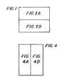
- FIG. 1 diagrams the relationship between FIGS. 1A, 1B;
- FIGS. 1A, 1B are symbolic representations of a read-only memory according to the invention;
- FIG. 2 is a diagrammatical view of a portion of the memory array used in the read-only memory shown in FIG. 1;
- FIG. 3 is a cross-section elevation view taken along line 3-3 of FIG. 2;
- FIG. 4 diagrams the relationship between FIGS. 4A, 4B;
- FIGS. 4A, 4B are schematic diagrams of the address and virtual ground decoder according to the invention;
- FIG. 5A is a schematic diagram of a memory cell programmed to have transistor action, storing a logical 0; and
- FIG. 5B is a schematic diagram of a memory cell programmed to have transistor action inhibited, storing a logical 1.
- Referring to FIGS. 1, 1A, 1B, a semiconductor integrated circuit memory (ROM) 10 is shown to include: an
array 12 ofmemory cells 14, arranged in pairs 17. Thememory cells 14 are arranged in a matrix of 2mrows 71 and n columns (not numbered), as shown, storing 2m by n bit digital words, where m is the number of bits used to address theROM 10. Corresponding with eachrow 71 are a pair of 2m-1 select lines SL₀ʹ-SL(2m-1)ʹ. One of the pair of corresponding select lines SL₀ʹ-SL(2m-1)ʹ is connected to a first one of thememory cells 14 in each pair 17 and the second one of the pair of corresponding select lines SL₀ʹ-SL(2m-1)ʹ is connected to the other one of thememory cells 14 in the pair 17. It is next noted that a pair of adjacent row lines RL₀-RL(2m-1) is disposed between successive select lines SL₀ʹ-SL(2m-1)ʹ and each row line RL₀-RL(2m-1) couples to eachmemory cell 14 incorresponding rows 71. Thememory 10 also includes: an address andselect line decoder 16; asense amplifier section 18; and a ROM enablecircuit 62. The address andselect line decoder 16 will be discussed in more detail in correction to FIG. 4. Suffice it to say here, however, thatdecoder 16, enables, or addresses, one of 2m row conductors (i.e., row lines RL₀-RL(2m-1), as shown, selectively in accordance with address signals on lines A₀-Am-1. More particularly,decoder 16 drives all but one of the row lines RL₀-RL(2m-1) "low" (to ground) while driving the enabled or addressed row line RL₀-RL(2m-1) "high" (+VDD). In addition, the address and selectline decoder 16 enables, or addresses, a selected two of the select SL₀ʹ-SL(2m-1)ʹ, corresponding to the enabled row line RL₀-RL(2m-1) during a read of the ROM. Column conductors, or bit lines BL₀-BL(n-1), carry the binary data accessed in addressedmemory cells 14 to thesense amplifier section 18 to thereby read from thememory cell array 12 the n-bits of the addressed one of the 2m+1 n-bit digital words stored insuch ROM 10; such digital words having been masked programmed into theROM 10 during its fabrication as an integrated circuit. Here the sense amplifiers in thesense amplifier section 18 are of a conventional design, each one thereof being coupled to a corresponding one of the bit lines BL₀-BL(n-1) to produce at the output of suchsense amplifier section 18 an n-bit digital word O₀-O(n-1). Thesense amplifier section 18 and address andselect line decoder 16 are controlled by the ROM enablecircuitry 62 by the enable signal online 64. An external input chip enable signal fed to input 60 controls ROM enablecircuitry 62 by enabling ROM enablecircuitry 62 when a ROM read cycle is requested (input 60 is "high") and disabling it when in the standby mode (input 60 is "low"). Referring now to a memory cell pair 17, eachmemory cell 14 in that pair 17 has anoutput terminal 32, enable terminal 30 and anaddress terminal 31 disposed between theenable terminal 30 and theoutput terminal 32. Theoutput terminals 32 in each memory cell pair 17 are coupled to acommon output terminal 24, which are in turn coupled to a corresponding bit line BL₀-BL(2n-1). Theaddress terminals 31 of all thememory cells 14 in eachmemory cell row 71 are coupled to a corresponding one of the row lines RL₀-RL(2m-1). The select lines SL₀ʹ-SL(2m-1)ʹ are disposed adjacent to alternatingmemory cell rows 71. The enableterminal 30 of a first one of thememory cells 14 in each memory cell pair 17 couples to a first one of the adjacent select lines SL₀ʹ-SL(2m-1)ʹ and the enableterminal 30 of the second one of thememory cells 14 of the pair 17 couples to a different one of the adjacent select lines SL₀ʹ-SL(2m-1)ʹ. Because eachmemory cell 14 of each memory cell pair 17 is coupled to a different one of the select lines SL₀ʹ-SL(2m-1), when the corresponding row line RL₀-RL(2m-1) is enabled, the binary data stored in one of thememory cells 14 is passed to thecommon output terminal 24. Therefore, twomemory cells 14 coupled to acommon output terminal 24 cannot be enabled simultaneously. - Referring to FIGS. 5A, 5B, the contents of the
memory cells 14 are shown. Here each memory cell 14 (FIGS. 1A, 1B) is an n-channel enhancement mode metal oxide semiconductor (MOS) field effect transistor (FET). Theoutput terminal 32 couples to the drain D, the enable terminal 30 couples to the source S and theaddress terminal 31 couples to the gate G of the FET. Each one of the cells 14 (FIGS. 1A, 1B) is programmed to have transistor action (to store a logic 0), as shown in FIG. 5A, or is programmed not to have transistor action (to store a logic 1) as shown in FIG. 5B. Transistor action occurs where signals on theaddress terminal 31 can control the conductivity between the drain D and the source S (FIG. 5A). Transistor action is inhibited where signals on theaddress terminal 31 cannot control the conductivity (FIG. 5B). When transistor action is inhibited, a high impedance state exists between the source S and drain D. Whencell 14a is enabled, a low impedance state exists between the drain D and the source S. - Referring back to FIGS. 1A, 1B, during operation of
ROM 10 while not being read (standby mode), the ROM enablecircuitry 62, controlled byinput 60 being "low", puts theROM 10 in a pre-charge state by placing a disable signal online 64. In the pre-charge state, address andselect line decoder 16 is disabled so that all the row lines RL₀-RL(2m-1) are "low" (ground) and all the select lines SL₀ʹ-SL(2m-1)ʹ are "high" (+VDD). Further, while in the pre-charge state, the disable signal online 64 disables the sense amplifiers in thesense amplifier section 18 to pre-charge the bit lines BL₀-BL(n-1) to +VDD. When a read cycle is desired, theinput 60 is "high", the ROM enablecircuit 62 sends an enable signal online 64, releasing the address andselect line decoder 16 and the sense amplifiers insense amplifier section 18 to access the desiredmemory cells 14. Operation of theROM 10 during a read cycle, while referring specifically, by way of example, to enable signals on row line RL₁, select lines SL0,1 and SL2,3, and an exemplary pair of memory cells 17a connected to bit line BL₁, it is first noted that an enable signal on row line RL₁ (a "high") and select line SL2,3 (a "low") places thememory cell 14a‴ into a conduction condition (having been programmed with transistor action), to discharge the stored charge over bit line BL₁ from +VDD toward ground. This reduction in voltage from +VDD is detected by the sense amplifier coupled to bit line BL₁ as a logical 0. It is noted that allother memory cells 14 coupled to bit line BL₁ will not have any effect on bit line BL₁, because all other row lines RL₀, RL₂-RL(2m-1) will be "low" thereby inhibiting the enabling of thoseother memory cells 14. When an enable signal is placed on row line RL₁ and select line SL0,1,memory cell 14b‴ is accessed, but transistor action incell 14b‴ is inhibited. Therefore, the voltage on bit line BL₁ stays at +VDD, indicating a logical 1 to the sense amplifiers insense amplifier section 18. - Referring now to FIGS. 2 and 3, it is noted that FIG. 3 is a cross-sectional view along the 3-3 line in FIG. 2. It is additionally noted that each one of the
memory cells 14 are formed in different regions of the semiconductor body used to fabricate theROM 10 as an integrated circuit. During fabrication of theROM 10 as an integrated circuit, those memory cells which are to store a logic 0 data bit have formed in that element an FET having transistor action, designated here as 14a (FIG. 5A). Amemory cell 14 that stores a logical 1 by having its transistor action is designated as 14b (FIG. 5B). - Referring to FIG. 3, N+
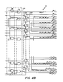
type conductivity regions 33a and 34a, 34c, forming the source S and drain D ofcells conductivity silicon substrate 41. Referring to FIGS. 2 and 3, the row lines RL₀-RL(2m-1) consist of doped polycrystalline silicon (polysilicon), with portions thereof providing gate electrodes G (FIGS. 5A, 5B). Further, as described above, the gate electrode G (FIG. 5A) ofmemory element 14a is disposed over a thin silicondioxide insulating layer 42 in etched area 50 (FIG. 3) of silicon dioxide on the portions of the surface of the well 40 between theregions 33a and 34a to provide an n-channel enhancement mode FET. A thick portion of silicondioxide insulating layer 42 is formed between the regions 33a, 34c to destroy any gate channel between such regions 33a, 34c and thus inhibit transistor action between regions 33a, 34c. It is here noted that while the use of a thick oxide layer between the source and drain regions to prevent transistor action has been described, other conventional techniques can be used to prevent such transistor action, such as active area removal or implantation into the channel region to raise the transistor threshold for conducting current. The bit lines BL₀-BL(n-1) are formed by a first level of metallization insulated from the polysilicon row lines RL₀-RL(2m-1) byoxide layer 43, and are arranged perpendicularly to the row lines RL₀-RL(2m-1). The select lines SL₀ʹ-SL(2m-1)ʹ are formed by a second level of metallization insulated from the bit lines BL₀-BL(n-1) byoxide layer 44, and are arranged to parallel the row lines RL₀-RL(2m-1). These select lines SL₀ʹ-SL(2m-1)ʹ are coupled to corresponding n+type conductivity regions 33 via contacts 36, such regions being diffused within well 40. It is further noted that in an actual realization of this ROM, the second level of metallization first couples to a first level of metallization which, in turn, couples to the n+ type conductivity region instead of directly going from a second level of metallization to the n+ type conductivity region as shown. For simplicity and clarity, the direct coupling from the second level metal to the n+ type conductivity region is shown. The bit lines BL₀-BL(n-1), deposited over n+ regions 34, are coupled thereto via contacts 37, such regions being diffused within well 40. The select lines SL₀ʹ, SL(2m-1)ʹ are arranged in rows such that they cross the semiconductor bulk comprising the ROM array over where the bit lines BL₀-BL(n-1) couple to the n+ region contacts 37. The columns of bit lines BL₀-BL(n-1) and the rows of select lines SL₀ʹ-SL(2m-1)ʹ form rows and columns ofregions 70, eachregion 70 having four memory cells 14 (FIGS. 1A, 1B). Rows and columns of theseregions 70 form rows and columns of common enable terminals 36. The address terminals 31 (FIGS. 1A, 1B) for each memory cell inregion 70 are disposed between the common select terminal 36 and each of the output terminals by the polysilicon row lines RL₀-RL(2m-1). A row 72 ofregions 70 with common enable terminals 36 has first alternating ones of the common enable terminals coupling to an adjacent select line SL₀ʹ-SL(2m-1)ʹ and second alternating ones of the common enable terminals 36 coupling to a different, adjacent select line SL₀ʹ-SL(2m-1)ʹ. For example, in a selected row 72a (see also row 72a in FIGS. 1A, 1B), a n+ region 33a in the center of region 70a forms a common source S (FIGS. 5A, 5B) via contact 36a (terminals 23 in FIGS. 1A, 1B) for each of the four memory cells (14a, 14b, 14bʹ, 14bʺ). Then+ regions 34a-34d at the corner of the region 70a, which couple to bit lines BL₀, BL₁ via contacts 37a-37d (terminals 24 in FIGS. 1A, 1B), form the drain D (FIGS. 5A, 5B). Terminal 36a couples to select line SL2,3 whileadjacent regions 70 in row 72a couple to a different, adjacent select line SL4,5. Row lines RL₃ and RL₄ form the address terminals 31 (FIGS. 1A, 1B) and gates G (FIGS. 5A, 5B) for cells 14aʹ, 14b ʹ andcells - Referring to FIGS. 4A, 4B, the address and select line decoder 16 (FIGS. 1A, 1B) is diagrammed. A conventional decoder 100 selects one of the outputs S₀,₁-S(2m-2),(2m-1) in response to the address line inputs A₁-Am-1. More specifically, the conventional decoder 100 contains two one-of-
N decoders 110, 111, each of which respond to separate sets of address inputs, here one-of-N decoder 110 responds to address Aj-Am-2 and one-of-N decoder 111 responds to address A₁-Aj-1. The outputs of the one-of-N decoders (112 fordecoder decoders 110 and 111 are "high") and the selected one of each of theoutputs array 115 logically ANDs (negative logic) theoutputs decoder array 120, in response to the select input S to thedecoder array 120. The input S is coupled to the address line input A₀. For example, if decoder 100 output S₀,₁ is "high" and A₀ is "low", decoder 120a, having its select input S "low", would enable RL₀. Conversely, if A₀ is "high", then RL₁ would be enabled. During a ROM read cycle, one of the row lines RL₀-RL(2m-1) is "high" corresponding to the state of the A₀ address input and the enabled one of the outputs S₀,₁-S(2m-2), (2m-1). The outputs S₀,₁-S(2m-2), (2m-1) from the conventional decoder 100 also couple to a NORarray 130 which enables a select one of a plurality of row line group select signals GS₀-GS(2m-2), (2m-1). These group select signals designate that a row line RL₀-RL(2m-1) in its corresponding group will be enabled. For example, group select signal GS0,1,2,3,4,5 being enabled (by being "low"), indicates that one of the row address lines RL₀-RL₅ will be active. These group select signals then couple to aNAND array 140 which enables a selected one of the plurality of select lines SL₀ʹ-SL(2m-1)ʹ which corresponds to the selected one of the row address lines RL₀-RL(2m-1). The first group ofNAND gates 144 in theNAND array 140 logically ORs together those group select signals GS₀-GS(2m-2),(2m-1) corresponding to the enabled select lines SL₀-SL(2m-1). For example, NAND gate 144b responds to group select signal GS₀, GS0,1,2,3,4,5 and GS6,7,8,9because select address line SL0,1 and select address line SL4,5, which are coupled to NAND gate 144b viaNAND gate 154b, correspond to row lines RL₀, RL₁, RL₂ and row lines RL₃, RL₄, RL₅, RL₆, respectively. Row line RL₀-RL(2m-1) which corresponds to a given select line SL₀ʹ-SL(2m-1)ʹ is shown in parentheses next to the select address line number. A further example is NAND gate 144c being responsive to group select GS0,1,2,3,4,5 and group select GS6,7,8,9 which couples viaNAND gate 154c to select address lines SL2,3 and SL6,7. Select address line SL2,3 corresponds to row lines RL₁, RL₂, RL₃, RL₄ and select line SL6,7 corresponds to row lines RL₅, RL₆, RL₇ and RL₈. The second group ofNAND gates 154 enables the select lines SL₀ʹ-SL(2m-1)ʹ such that two memory cells with a common enabled row address line RL₀-RL(2m-1) and common output terminal 37 (FIGS. 2, 3, corresponding to paired memory cells 17 in FIGS. 1A, 1B) will not be enabled to the same bit line BL₀-BL(n-1) (FIGS. 1A, 1B) simultaneously. This selection is accomplished by the address bit line Am and inverter 159 (which inverts the address bit line Am) coupling toNAND gates 154 to inhibit adjacent select lines SL₀ʹ-SL(2m-1)ʹ from simultaneously being enabled if they have identical corresponding row address lines RL₀-RL(2m-1) that are enabled (e.g. SL0,1 and SL2,3 both have corresponding row lines RL₁ and RL₂). It is noted that to avoid delays associated with decoding for the row line RL₀-RL(2m-1) and then deciding which select line SL₀ʹ-SL(2m-1)ʹ is to be enabled, simultaneous row and select line decoding is required. Hence, two stage address decoding for the row lines RL₀-RL(2m-1) (decoder 100 and decoder 120) provides a "look ahead", or advanced enabling, from decoder 100 for the select line decoders (NORarray 130, NAND array 140). - Having described a preferred embodiment of this invention, it will now be apparent to one of skill in the art that other embodiments incorporating its concept may be used. Therefore, it is believed that this invention should not be restricted to the disclosed embodiment, but rather should be limited only by the spirit and scope of the appended claims.
Claims (5)
a selected row of regions with common enable terminals having first alternating ones of the common enable terminals coupling to an adjacent corresponding one of the first plurality of row electrical conductors and second alternating ones of the common enable terminals coupling to a different, adjacent corresponding one of the first plurality of row electrical conductors.
a plurality of input address lines;
a pair of input address lines;
a decoder means, coupled to the plurality of input address lines, for enabling one of a plurality of outputs;
a first selecting means, responsive to the decoder means and a first one of the pair of input address lines, for enabling a select one of the plurality of row lines; and
a second selecting means, responsive to the plurality of outputs of the decoder means and a second one of the pair of input address lines, for enabling a select one of the plurality of select lines that corresponds to the selected row line.
means, responsive to the decoder means, for generating a select one of a plurality of row line group select signals, wherein the plurality of row address line select signals corresponds to the sets of row lines and that will be enabled by the first selecting means; and
a third selecting means, responsive to the plurality of row line group select signals and the second one of the pair of input address lines, for enabling a selected one of the plurality of select lines in correspondence to the select one of the plurality of row lines and the second one of the pair of input address lines.
Applications Claiming Priority (2)
| Application Number | Priority Date | Filing Date | Title |
|---|---|---|---|
| US81329085A | 1985-12-24 | 1985-12-24 | |
| US813290 | 1985-12-24 |
Publications (3)
| Publication Number | Publication Date |
|---|---|
| EP0227464A2 true EP0227464A2 (en) | 1987-07-01 |
| EP0227464A3 EP0227464A3 (en) | 1989-05-31 |
| EP0227464B1 EP0227464B1 (en) | 1992-05-06 |
Family
ID=25211985
Family Applications (1)
| Application Number | Title | Priority Date | Filing Date |
|---|---|---|---|
| EP86310023A Expired - Lifetime EP0227464B1 (en) | 1985-12-24 | 1986-12-22 | High density read-only memory |
Country Status (4)
| Country | Link |
|---|---|
| EP (1) | EP0227464B1 (en) |
| JP (1) | JPS62241370A (en) |
| CA (1) | CA1265868A (en) |
| DE (1) | DE3685206D1 (en) |
Citations (3)
| Publication number | Priority date | Publication date | Assignee | Title |
|---|---|---|---|---|
| DE2852049A1 (en) * | 1977-12-02 | 1979-06-07 | Tokyo Shibaura Electric Co | FIXED OR READ MEMORY |
| US4301518A (en) * | 1979-11-01 | 1981-11-17 | Texas Instruments Incorporated | Differential sensing of single ended memory array |
| US4314362A (en) * | 1980-02-04 | 1982-02-02 | Texas Instruments, Incorporated | Power down sequence for electrically programmable memory |
-
1986
- 1986-12-22 DE DE8686310023T patent/DE3685206D1/en not_active Expired - Fee Related
- 1986-12-22 EP EP86310023A patent/EP0227464B1/en not_active Expired - Lifetime
- 1986-12-23 CA CA000526168A patent/CA1265868A/en not_active Expired - Fee Related
- 1986-12-24 JP JP61316117A patent/JPS62241370A/en active Granted
Patent Citations (3)
| Publication number | Priority date | Publication date | Assignee | Title |
|---|---|---|---|---|
| DE2852049A1 (en) * | 1977-12-02 | 1979-06-07 | Tokyo Shibaura Electric Co | FIXED OR READ MEMORY |
| US4301518A (en) * | 1979-11-01 | 1981-11-17 | Texas Instruments Incorporated | Differential sensing of single ended memory array |
| US4314362A (en) * | 1980-02-04 | 1982-02-02 | Texas Instruments, Incorporated | Power down sequence for electrically programmable memory |
Non-Patent Citations (1)
| Title |
|---|
| ISSCC DIGEST OF TECHNICAL PAPERS, 16th February 1978, Session Xii: "High density memories", pages 152-153, IEEE, New York, US; D.R. WILSON et al.: "A 100ns, 150mW, 64Kbit ROM" * |
Also Published As
| Publication number | Publication date |
|---|---|
| EP0227464B1 (en) | 1992-05-06 |
| CA1265868A (en) | 1990-02-13 |
| JPH0563021B2 (en) | 1993-09-09 |
| JPS62241370A (en) | 1987-10-22 |
| EP0227464A3 (en) | 1989-05-31 |
| DE3685206D1 (en) | 1992-06-11 |
Similar Documents
| Publication | Publication Date | Title |
|---|---|---|
| EP0072845B1 (en) | Memory system having memory cells capable of storing more than two states | |
| US4980861A (en) | NAND stack ROM | |
| US5583808A (en) | EPROM array segmented for high performance and method for controlling same | |
| US4602354A (en) | X-and-OR memory array | |
| US5003205A (en) | Buffer circuit used in a semiconductor device operating by different supply potentials and method of operating the same | |
| KR0179361B1 (en) | Bitline segmentation in logic memory arrays c 16/06 | |
| EP0191544B1 (en) | Cmos decoder/driver circuit for a memory | |
| US4545035A (en) | Dynamic RAM with nonvolatile shadow memory | |
| US4719603A (en) | Semiconductor memory having a dynamic level detecting means for detecting a level of a word line | |
| US4599704A (en) | Read only memory circuit | |
| US6577521B2 (en) | Memory architecture and decoder addressing | |
| US5812453A (en) | Programmable semiconductor memory | |
| US4901285A (en) | High density read-only memory | |
| EP0095847B1 (en) | Compact rom with reduced access time | |
| US4634893A (en) | FET driver circuit with mask programmable transition rates | |
| US4636664A (en) | Current sinking responsive MOS sense amplifier | |
| US4402063A (en) | Flip-flop detector array for minimum geometry semiconductor memory apparatus | |
| JPS61267997A (en) | Semiconductor circuit | |
| US4057787A (en) | Read only memory | |
| EP0227464B1 (en) | High density read-only memory | |
| US20040119105A1 (en) | Ferroelectric memory | |
| EP0365720B1 (en) | Programmable semiconductor memory | |
| US4292547A (en) | IGFET Decode circuit using series-coupled transistors | |
| US5245566A (en) | Programmable semiconductor | |
| EP0275212B1 (en) | Nand stack rom |
Legal Events
| Date | Code | Title | Description |
|---|---|---|---|
| PUAI | Public reference made under article 153(3) epc to a published international application that has entered the european phase |
Free format text: ORIGINAL CODE: 0009012 |
|
| AK | Designated contracting states |
Kind code of ref document: A2 Designated state(s): BE DE FR GB IT NL |
|
| PUAL | Search report despatched |
Free format text: ORIGINAL CODE: 0009013 |
|
| AK | Designated contracting states |
Kind code of ref document: A3 Designated state(s): BE DE FR GB IT NL |
|
| 17P | Request for examination filed |
Effective date: 19890906 |
|
| 17Q | First examination report despatched |
Effective date: 19901206 |
|
| ITTA | It: last paid annual fee | ||
| GRAA | (expected) grant |
Free format text: ORIGINAL CODE: 0009210 |
|
| AK | Designated contracting states |
Kind code of ref document: B1 Designated state(s): BE DE FR GB IT NL |
|
| REF | Corresponds to: |
Ref document number: 3685206 Country of ref document: DE Date of ref document: 19920611 |
|
| ITF | It: translation for a ep patent filed |
Owner name: BARZANO' E ZANARDO ROMA S.P.A. |
|
| ET | Fr: translation filed | ||
| PGFP | Annual fee paid to national office [announced via postgrant information from national office to epo] |
Ref country code: FR Payment date: 19921126 Year of fee payment: 7 |
|
| PGFP | Annual fee paid to national office [announced via postgrant information from national office to epo] |
Ref country code: GB Payment date: 19921217 Year of fee payment: 7 |
|
| PGFP | Annual fee paid to national office [announced via postgrant information from national office to epo] |
Ref country code: NL Payment date: 19921231 Year of fee payment: 7 |
|
| PGFP | Annual fee paid to national office [announced via postgrant information from national office to epo] |
Ref country code: BE Payment date: 19930115 Year of fee payment: 7 |
|
| PLBE | No opposition filed within time limit |
Free format text: ORIGINAL CODE: 0009261 |
|
| STAA | Information on the status of an ep patent application or granted ep patent |
Free format text: STATUS: NO OPPOSITION FILED WITHIN TIME LIMIT |
|
| 26N | No opposition filed | ||
| PGFP | Annual fee paid to national office [announced via postgrant information from national office to epo] |
Ref country code: DE Payment date: 19930830 Year of fee payment: 7 |
|
| NLS | Nl: assignments of ep-patents |
Owner name: LITTON SYSTEMS, INC. TE WOODLAND HILLS, CALIFORNIE |
|
| PG25 | Lapsed in a contracting state [announced via postgrant information from national office to epo] |
Ref country code: GB Effective date: 19931222 |
|
| PG25 | Lapsed in a contracting state [announced via postgrant information from national office to epo] |
Ref country code: BE Effective date: 19931231 |
|
| BERE | Be: lapsed |
Owner name: RAYTHEON CY Effective date: 19931231 |
|
| PG25 | Lapsed in a contracting state [announced via postgrant information from national office to epo] |
Ref country code: NL Effective date: 19940701 |
|
| NLV4 | Nl: lapsed or anulled due to non-payment of the annual fee | ||
| GBPC | Gb: european patent ceased through non-payment of renewal fee |
Effective date: 19931222 |
|
| PG25 | Lapsed in a contracting state [announced via postgrant information from national office to epo] |
Ref country code: FR Effective date: 19940831 |
|
| PG25 | Lapsed in a contracting state [announced via postgrant information from national office to epo] |
Ref country code: DE Effective date: 19940901 |
|
| REG | Reference to a national code |
Ref country code: FR Ref legal event code: ST |
|
| PG25 | Lapsed in a contracting state [announced via postgrant information from national office to epo] |
Ref country code: IT Free format text: LAPSE BECAUSE OF NON-PAYMENT OF DUE FEES Effective date: 20051222 |