EP0227318B1 - Encryption/decryption system - Google Patents
Encryption/decryption system Download PDFInfo
- Publication number
- EP0227318B1 EP0227318B1 EP86309231A EP86309231A EP0227318B1 EP 0227318 B1 EP0227318 B1 EP 0227318B1 EP 86309231 A EP86309231 A EP 86309231A EP 86309231 A EP86309231 A EP 86309231A EP 0227318 B1 EP0227318 B1 EP 0227318B1
- Authority
- EP
- European Patent Office
- Prior art keywords
- signal
- random number
- frame
- bits
- memory
- Prior art date
- Legal status (The legal status is an assumption and is not a legal conclusion. Google has not performed a legal analysis and makes no representation as to the accuracy of the status listed.)
- Expired - Lifetime
Links
Images


Classifications
-
- H—ELECTRICITY
- H04—ELECTRIC COMMUNICATION TECHNIQUE
- H04L—TRANSMISSION OF DIGITAL INFORMATION, e.g. TELEGRAPHIC COMMUNICATION
- H04L9/00—Cryptographic mechanisms or cryptographic arrangements for secret or secure communications; Network security protocols
- H04L9/06—Cryptographic mechanisms or cryptographic arrangements for secret or secure communications; Network security protocols the encryption apparatus using shift registers or memories for block-wise or stream coding, e.g. DES systems or RC4; Hash functions; Pseudorandom sequence generators
- H04L9/065—Encryption by serially and continuously modifying data stream elements, e.g. stream cipher systems, RC4, SEAL or A5/3
- H04L9/0656—Pseudorandom key sequence combined element-for-element with data sequence, e.g. one-time-pad [OTP] or Vernam's cipher
- H04L9/0662—Pseudorandom key sequence combined element-for-element with data sequence, e.g. one-time-pad [OTP] or Vernam's cipher with particular pseudorandom sequence generator
-
- H—ELECTRICITY
- H04—ELECTRIC COMMUNICATION TECHNIQUE
- H04L—TRANSMISSION OF DIGITAL INFORMATION, e.g. TELEGRAPHIC COMMUNICATION
- H04L9/00—Cryptographic mechanisms or cryptographic arrangements for secret or secure communications; Network security protocols
- H04L9/12—Transmitting and receiving encryption devices synchronised or initially set up in a particular manner
-
- H—ELECTRICITY
- H04—ELECTRIC COMMUNICATION TECHNIQUE
- H04L—TRANSMISSION OF DIGITAL INFORMATION, e.g. TELEGRAPHIC COMMUNICATION
- H04L2209/00—Additional information or applications relating to cryptographic mechanisms or cryptographic arrangements for secret or secure communication H04L9/00
- H04L2209/12—Details relating to cryptographic hardware or logic circuitry
- H04L2209/125—Parallelization or pipelining, e.g. for accelerating processing of cryptographic operations
-
- H—ELECTRICITY
- H04—ELECTRIC COMMUNICATION TECHNIQUE
- H04L—TRANSMISSION OF DIGITAL INFORMATION, e.g. TELEGRAPHIC COMMUNICATION
- H04L2209/00—Additional information or applications relating to cryptographic mechanisms or cryptographic arrangements for secret or secure communication H04L9/00
- H04L2209/34—Encoding or coding, e.g. Huffman coding or error correction
Definitions
- This invention relates to devices for providing message secrecy and more particularly to an encryption/decryption system for insertion in a digitalized communication channel to maintain message privacy.
- Communication channels are increasingly being used to transmit highly confidential and important data and messages between and within businesses.
- the need to safeguard such data from eavesdropping and unauthorized tampering has grown correspondingly.
- One traditional protection technique is to encrypt the data at the transmitting end and decrypt it at the receiving end.
- certain conventional systems employ nonlinear encryption by storing a controlling encryption key variable at the transmitting and receiving ends and using a technique in which the encryption at a later time depends on the encrypted message at an earlier time.
- Such systems have an exceptionally high level of message secrecy.
- the encryption key variable can become rather slow in recovering from transmission errors in the received encrypted signal. Each transmission error interferes with correct decoding, causing a blackout period during which it is impossible to correctly decrypt a corresponding portion of the message. Enabling the encryption key variable to have a greater variety of possible values lengthens the blackout period.
- an object of this invention is to provide a new and improved encryption/decryption system which enables the encryption key variable to have a larger variety of possible values without greatly increasing the errors in the decoded signal reproduced at the receiving end. Yet another object is to provide such a device with a very high level of message secrecy without sacrificing relatively simple construction and moderate cost.
- an encryption/decryption system for a communication channel encrypts an input digital signal at the transmitting end and reproduces it at the receiving end.
- the transmitting end of the system has a first storage register, a first memory, a first selector device, and an encrypted signal composing device.
- the encrypted signal composing device combines a randomized coding signal with the input digital signal to form an encrypted signal segmented into frames.
- the invention uses cipher feedback.
- the first storage register stores bits of the encrypted signal and outputs them in parallel.
- the first memory receives these parallel bits as addresses and outputs corresponding random numbers.
- the first selector device selects from the random number data to form the randomized coding signal fed to the encrypted signal composing device.
- the receiving end has a second storage register, a second memory, a second selector device, and a digital signal reproducing device.
- the second storage register stores bits of the received encrypted signal and outputs them in parallel.
- the second memory receives these parallel bits as addresses and outputs corresponding random numbers. To enable decoding, the working and stored contents of the first and second memories are identical.
- the second selector device operating the same way as the first, selects from the random number data to form a decoding signal.
- the digital signal reproducing device combines the received encrypted signal with the randomized decoding signal to reproduce the input digital signal.
- FIG. 4 An example of a prior art encryption device employed in a communications transmitting system is shown in Fig. 4.
- Fig. 5 shows a complementary prior art decryption device employed in a communications receiving system.
- a digital input signal S is combined by an Exclusive OR (XOR) gate 2 with a randomized digital encoding signal Y successively output from a transmitter memory unit 1. This produces an encrypted signal Z for transmission.
- XOR Exclusive OR
- the successive bits of the encrypted digital signal Z are input for temporary storage to an M bit shift register 3 as shift register bits R1, R2, ..., R M .
- Memory unit 1 has 2 M addresses, each of which contains a prestored random bit, a logical 0 or 1.
- the register bits R1, R2, ..., R M are then used in parallel as an input address to memory unit 1, which outputs the prestored random bit at that address as the next bit of Y.
- the encrypted digital signal Z is input to a transmitter 4, which transmits it whenever a transmission switch 5 is closed.
- a received digital signal Z' is output by a receiver 9.
- the received signal Z' is input to an M bit shift register 6 as shift register bits R'1, R'2, ..., R' M .
- a receiver memory unit 7 has 2 M addresses, each of which contains a prestored bit.
- the register bits R'1, R'2, ..., R' M are then used in parallel as an input address to memory unit 7, which outputs the prestored random bit at that address as the next bit of a decoding signal Y'.
- the received signal Z' is successively combined by an Exclusive OR (XOR) gate 8 with the decoding signal Y' to generate a reproduced signal S'.
- XOR Exclusive OR
- the prestored random bits of the receiver memory unit 7 of the receiving system are made identical to those stored in the corresponding addresses of the transmitter memory unit 1 of the transmitting system.
- Z' Z
- the encryption and decryption operations are controlled by the particular random bit pattern stored in the addresses in memory units 1 and 6. This important controlling bit pattern is called the encryption key variable.
- Such conventional encryption/decryption devices have the advantages of simple construction and, because they use nonlinear encryption, an exceptionally high level of message secrecy.
- they have the disadvantage that increasing the number of possible random bit patterns that might be stored in the memories 1 and 7, that is enabling the encryption key variable to have a larger variety of possible values, also increases the system's weakness with respect to transmission errors.
- increasing the number of possible random bit patterns that might be stored in the memories 1 and 7, that is enabling the encryption key variable to have a larger variety of possible values also increases the system's weakness with respect to transmission errors.
- the number of bits M used in shift registers 3 and 6 must be increased to add more addresses.
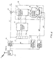
- Fig. 1 shows a block diagram of a first embodiment of an encryption system that overcomes these problems for use at the transmitting end of a communications link.
- An XOR (Exclusive OR) gate 10 combines an input digital signal S with a randomized coding signal Y to produce an encrypted digital signal Z.
- a shift register 12 receives and temporarily stores the successive bits of signal Z as register bits r1, r2, ..., r m .
- the m register bits are then provided in parallel as an input memory address to a transmitter memory unit 22.
- Each of the 2 m addresses in memory unit 22 is prestored with a corresponding n bit random number x1, x2, ..., x n .
- the number n is an integer equal to or greater than 2.
- encoder memory 22 outputs its corresponding stored random number x1, x2, ..., x n .
- Random selection circuit 11 selects from among the n bit random number data x1, x2, ..., x n output by memory unit 22 to form each frame of bits of the coding signal Y.
- Random selection circuit 11 comprises an encoder frame counter 15, an encoder memory 14, and an encoder selector circuit 13.
- a frame pulse FP output by a frame sync pulse generator 16 is input as a clock signal to counter 15, which has q bits.
- the counter bits b1, b2, ..., b q are provided in parallel as an input memory address to the encoder memory 14.
- Each of the 2 q addresses in encoder memory 14 is prestored with a corresponding p bit random number a1, a2, ..., a p .
- the random number a1, a2, ..., a p stored at address b1, b2, ..., b q is output to selector circuit 13 to change its selection contents.
- encoder counter 15 and encoder memory 14 together form a random number generator, generating a random number for the selector circuit 13 for each frame of the signal.
- a PN pseudo-noise
- PN pseudo-noise
- Encoding circuit 13 receives each of the n bit random numbers x1, x2, ..., x n output by transmitter memory unit 22. Based on the value of random number a1, a2, ..., a p for the current frame, random selection circuit 13 selects from among the n bit random number data x1, x2, ..., x n output by memory unit 22 to form each frame of bits of the coding signal Y. Signal Y is then combined with input signal S by XOR gate 10 to produce the encrypted digital signal Z.
- the encrypted signal Z is input to a frame composing circuit 19, which combines it with a frame sync signal FS and a START signal prefix to produce a TDATA signal for transmission.
- the frame sync signal FS is generated by a frame sync signal generator 17 in response to a frame sync pulse FP from pulse generator 16.
- the START signal prefix is generated by a start signal generator 18 in response to the closing of a transmission switch 21.
- the TDATA signal is then transmitted by a transmitter 20.
- Transmission switch 21 is arranged so that, when it is closed, it activates transmitter 20. When switch 21 is first closed, it also sends encoder counter 15 a Clear signal to set it to a preselected initial value.
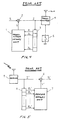
- Figure 3 shows the make-up of each frame of the TDATA signal output as well as its relationship in time to its corresponding frame sync pulse.
- "START” indicates the START signal
- "FS” the frame sync signal
- "Z” the encrypted signal Z
- "FP" the frame sync pulse.
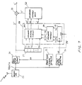
- Figure 2 shows a block diagram of a first embodiment of a decryption system for receiving the signal transmitted by the system of Fig. 1 and reproducing from it the input digital signal S.
- a receiver 23 picks up the transmitted signal of Fig. 3 and outputs a received digital signal RDATA.
- Signal RDATA is input to a separator circuit 24, a frame sync signal detector 25, and start signal detector 26.
- Separator circuit 24 separates out a received encrypted signal Z' from the received signal RDATA. If there have been no errors in the transmission path, this signal Z' is identical to the transmitted encrypted digital signal Z.
- detector 26 detects the START signal prefix at the beginning of the RDATA signal and outputs a start pulse SP.
- Frame sync signal detector 25 detects each frame signal FS and outputs a frame sync pulse FP.
- the frame pulses FP output by detector 25 are used to synchronize separating circuit 24 so that for each frame it can separate out just the signal Z' which corresponds to the Z portion of the transmitted signal of Fig. 3.
- the frame pulse FP is also provided as a clock signal to a decoder frame counter 31 in a decoder random selection circuit 28.
- the start pulse SP from detector 26 is provided as a Clear signal to counter 31 to set it to a preselected initial value.
- the encrypted received signal Z' output by circuit 24 is input to both a shift register 27 and an XOR gate 33.
- Shift register 27 receives and temporarily stores the successive bits of signal Z' as register bits r'1, r'2, ..., r' m . These m register bits are then provided in parallel as an input memory address to a receiver memory unit 32.
- Each of the 2 m addresses in memory unit 32 is prestored with a corresponding n bit random number x'1, x'2, ..., x' n .
- the random number x'1, x'2, ..., x' n stored at that address is output.
- a decoder selector circuit 29 in random selection circuit 28 receives and selects from among the n bit random number data x'1, x'2, ..., x' n output by memory unit 32 to form each frame of bits of a decoding signal Y'.
- Signal Y' is then provided to the XOR gate 33.
- Decoder random selection circuit 28 works exactly like the encoder random selection circuit 11 in the encryption system at the transmitting end.
- Decoder counter 31 is initialized by a start pulse SP from detector 26 before counting the frame sync pulses FP output by detector 25.
- the output b'1, b'2, ..., b' q of counter 31 is provided in parallel as address input to a decoder memory 30 for each frame. This outputs a stored random number a'1, a'2, ..., a' p for each address.
- the random number output a'1, a'2, ..., a' p controls the selection contents of decoder selector circuit 29 for each frame.
- random selection circuit 29 selects from among the n bit random number data x'1, x'2, ..., x' n output by memory unit 32 to form each frame of bits of the decoding signal Y' for XOR gate 33.
- the XOR gate 33 then combines encrypted received signal Z' with decoding signal Y' to reproduce digital signal S' as the decrypted message signal.
- Counter 15 at the transmitting end and counter 31 at the receiving end are each set to the same preselected initial value before they begin counting frame sync pulses.
- Decoder memory 30 is prestored with the same pattern of random numbers prestored in encoder memory 14. This enables decoder random selection circuit 28 to follow the identical selection routine employed by encoder random selection circuit 11.
- Receiver memory unit 32 is prestored with the same pattern of random numbers prestored in transmitter memory unit 22. Therefore, when there are no transmission errors, the reproduced digital signal S' at the receiver end is identical to the digital signal S input at the transmitting end. For no transmission errors, this result is just as in the prior art encoder/decoder system.
- the logical working of the decoding mechanism is as follows. When no errors are introduced by the transmission path, the received signal Z' equals the encrypted cipher signal Z. Then shift registers 27 and 12 provide the same address inputs to memory units 32 and 22, having identical contents. Each random number x'1, x'2, ..., x' n output by receiver memory unit 32 is identical to the random number x1, x2, ..., x n previously output by transmitter memory unit 22.
- decoder random selection circuit 28 can duplicate the working of encoder random selection circuit 11. This enables randomized signal Y' to be identical to randomized signal Y.
- shift registers 12, 27 to have only m bits, where m is less than the usual M bits used in prior art shift registers 3 and 6 of Figs. 4 and 5. If an error is generated in the transmission path, it causes errors in the decoding signal Y' for a time interval equal to the time it takes to transmit m bits. However, because the number of bits m in register 27 can be less than the usual M bits, the amount of time that the received signal S' is not properly reproduced is reduced.
- the number of bits n stored at each memory address can be selected to be a relatively small number as compared to the address length m, reducing the complexity of encoder selector circuit 13 and decoder selector circuit 29.
- the variety of random numbers stored in the encoder memory 14 and decoder memory 30 can be made very large. This effectively gives the encryption key variable a large number of possible values without increasing the errors in decoding signal Y' or the reproduced digital signal S'.
- the present invention not only randomizes individual signal bits in the transmitted signal but also changes the selection rule used by encoder random selection circuit 11 to form encoding signal Y for each frame of the message. This ensures an exceptionally strong level of message secrecy without greatly increasing the errors in reproduced digital signal S'. The number of different values for the encryption key variable of the coder/encoder is greatly increased without sacrificing the system's prompt recovery from any transmission channel errors.
- a cipher feedback loop comprising, in order, a register (12), a transmitter memory unit (22), and a random selection circuit (11) provides the randomized coding signal Y.
- the decoding signal Y' is provided by a cipher feedback loop comprising, in order, a register (27), a transmitter memory unit (32), and a random selection circuit (28).
- Fig. 6 shows a second embodiment of the inventive encryption system having a different cipher feedback loop comprising, in order, a shift register 12, a random selection circuit 41, and a transmitter memory unit 42.
- the remaining portions of the second embodiment of the encryption system are identical to those shown in Fig. 1 for the first embodiment, as indicated by use of identical reference numerals.
- shift register 12 stores and outputs in parallel a predetermined number of bits m of the encrypted signal Z output from the XOR gate 10. For each signal frame, random selection circuit 41 randomly selects from among the m bit number data output by shift register 12 and outputs corresponding n bit address numbers w1, w2, ..., w n , where n is an integer equal to or greater than 2.
- Transmitter memory unit 42 receives the n bit addresses and for each address w1, w2, ..., w n outputs a corresponding random bit prestored at the address. The successive bits output by memory unit 42 make up the randomized coding signal Y.
- Random selection circuit 41 has a frame counter 45 fed by frame sync pulses FP from a frame sync pulse generator 16.
- the output of frame counter 45 is a q bit number b1, b2 ..., b q for each frame.
- An encoder memory 44 receives the q bit output of counter 45 as an address. It outputs a p bit random number a1, a2, ..., a p prestored at that address to a selector circuit 43 which executes the selection made by selection circuit 41.
- the selection rule of selector circuit 43 is controlled by the value of random number a1, a2, ..., a p for the current frame. In effect, counter 45 and encoder memory 44 generate a p bit random number a1, a2, ..., a p for each frame for controlling selector circuit 43.
- Fig. 7 shows a second embodiment of the inventive decryption system for use at the receiving end of a communications link to decode signals transmitted by the system of Fig. 6.
- This decryption system has a cipher feedback loop comprising, in order, a shift register 27, a random selection circuit 58, and a receiver memory unit 52.
- the remaining portions of the second embodiment of the decryption system are identical to those shown in Fig. 2 for the first embodiment, as indicated by use of identical numerals.
- shift register 27 stores and outputs in parallel a predetermined number of bits m of the received encrypted signal Z' output from separating circuit 24.
- the selection circuit 58 selects from among the m bit number data output by shift register 27 and outputs corresponding n bit address numbers w'1, w'2, ..., w' n .
- Receiver memory unit 52 has stored contents identical to that of transmitter memory unit 42 (Fig. 6). Memory unit 52 receives the n bit addresses and for each address w'1, w'2, ..., w' n outputs a corresponding random bit (0 or 1) prestored at the address. The successive bits output by memory unit 52 make up the decoding signal Y'.
- Selection circuit 58 operates the same way as random selection circuit 41 and in sync with a corresponding frame of the encrypted signal Z.
- Circuit 58 has a frame counter 51 fed by frame sync pulses from a frame sync signal detector 25.
- the output of frame counter 51 is a q bit number b'1, b'2 ..., b' q for each frame.
- a decoder memory 50 has stored contents identical to that of encoder memory 44 (Fig. 6).
- Decoder memory 50 receives the q bit output of counter 51 as an address. It outputs a p bit number a'1, a'2, ..., a' p prestored at that address to a selector circuit 59 which executes the selection made by selection circuit 58.
- the selection rule of selector circuit 59 is controlled by the value of random number a'1, a'2, ..., a' p for the current frame.
- counter 51 and decoder memory 50 generate a p bit number a'1, a'2 .., a' p for each frame for controlling selector circuit 59.
- the remaining portions of the second embodiment of the decryption system function like those shown in Fig. 2 for the first embodiment, their working will not again be described.
- the stored contents and working of the decryption system are chosen to replicate those of the encryption system.
- the received encrypted signal Z' equals the encrypted signal Z
- the decoding signal Y' equals the randomized encoding signal Y.
- the second embodiment of the encryption and decryption systems enables the number of values for the encryption key variable to be increased without increasing the number of bits m used in the shift registers 12 and 27. Instead, the additional randomizing key information is provided in the encrypter by the working of selector circuit 43, transmitter memory 42, encoder memory 44, and frame counter 45, and their counterparts in the decryption system.
- the number of bits n in address numbers w1, w2, ..., w n and w'1, w'2, ..., w' n can be selected to be a relatively small number as compared to the address length m, reducing the complexity of transmitter memory unit 42 and receiver memory unit 52.
- an address may be incremented by means of frame sync signals, the intervals between which may constitute an information data word.
Landscapes
- Engineering & Computer Science (AREA)
- Computer Security & Cryptography (AREA)
- Computer Networks & Wireless Communication (AREA)
- Signal Processing (AREA)
- Transmission Systems Not Characterized By The Medium Used For Transmission (AREA)
- Mobile Radio Communication Systems (AREA)
- Two-Way Televisions, Distribution Of Moving Picture Or The Like (AREA)
- Time-Division Multiplex Systems (AREA)
Description
- This invention relates to devices for providing message secrecy and more particularly to an encryption/decryption system for insertion in a digitalized communication channel to maintain message privacy.
- Communication channels, particularly radio communication links, are increasingly being used to transmit highly confidential and important data and messages between and within businesses. The need to safeguard such data from eavesdropping and unauthorized tampering has grown correspondingly. One traditional protection technique is to encrypt the data at the transmitting end and decrypt it at the receiving end.
- In the specification of U.S. Patent No. 4,447,672, which was published on May 8 1984, there are proposed an encrypting and a decrypting device similar to those shown in Figs. 4 and 5 of the accompanying drawings to be described below.
- A review article, which was published in 1982 in IEE PROC., Vol. 129 Pr. A No. 6 August 1982 pages 357 to 376, describes, with reference to a Fig. 15, a system in which two random variables, which are generated by two shift registers, are multiplexed. The generating sequences of neither of the two random variables is changed.
- However, previous efforts to safeguard data communications have had difficulty reconciling the need for a high level of secrecy with other important goals, such as simple construction and low cost, quick recovery from transmission errors, and minimum reduction of message throughput.
- For example, certain conventional systems employ nonlinear encryption by storing a controlling encryption key variable at the transmitting and receiving ends and using a technique in which the encryption at a later time depends on the encrypted message at an earlier time. Such systems have an exceptionally high level of message secrecy. However, if provision is made for the encryption key variable to have a large number of possible values, the conventional system can become rather slow in recovering from transmission errors in the received encrypted signal. Each transmission error interferes with correct decoding, causing a blackout period during which it is impossible to correctly decrypt a corresponding portion of the message. Enabling the encryption key variable to have a greater variety of possible values lengthens the blackout period.
- Accordingly, an object of this invention is to provide a new and improved encryption/decryption system which enables the encryption key variable to have a larger variety of possible values without greatly increasing the errors in the decoded signal reproduced at the receiving end. Yet another object is to provide such a device with a very high level of message secrecy without sacrificing relatively simple construction and moderate cost.
- In keeping with one aspect of the invention, an encryption/decryption system for a communication channel encrypts an input digital signal at the transmitting end and reproduces it at the receiving end. The transmitting end of the system has a first storage register, a first memory, a first selector device, and an encrypted signal composing device. The encrypted signal composing device combines a randomized coding signal with the input digital signal to form an encrypted signal segmented into frames.
- For additional protection, the invention uses cipher feedback. The first storage register stores bits of the encrypted signal and outputs them in parallel. The first memory receives these parallel bits as addresses and outputs corresponding random numbers. The first selector device selects from the random number data to form the randomized coding signal fed to the encrypted signal composing device.
- The receiving end has a second storage register, a second memory, a second selector device, and a digital signal reproducing device. The second storage register stores bits of the received encrypted signal and outputs them in parallel. The second memory receives these parallel bits as addresses and outputs corresponding random numbers. To enable decoding, the working and stored contents of the first and second memories are identical.
- The second selector device, operating the same way as the first, selects from the random number data to form a decoding signal. The digital signal reproducing device combines the received encrypted signal with the randomized decoding signal to reproduce the input digital signal.
- The above mentioned and other features of this invention and the manner of obtaining them will become more apparent, and the invention itself will be best understood, by reference to the following description of embodiments of the invention taken in conjunction with the accompanying drawings, in which:
- Fig. 1 is a block diagram of a first embodiment of an inventive encryption system for use at the transmitting end of a communications link;
- Fig. 2 is a block diagram of a first embodiment of an inventive decryption system for use at the receiving end of a communications link to decode signals transmitted from the system of Fig. 1;
- Fig. 3 is a timing chart for use in describing the operation of the systems of Figs. 1 and 2;
- Fig. 4 is a block diagram of a communications transmitting system employing a prior art encryption device;
- Fig. 5 is a block diagram of a communications receiving system employing a prior art decryption device;
- Fig. 6 is a block diagram of a second embodiment of the inventive encryption system for use at the transmitting end of a communications link; and
- Fig. 7 is a block diagram of a second embodiment of the inventive decryption system for use at the receiving end of a communications link to decode signals transmitted by the system of Fig. 6.
- An example of a prior art encryption device employed in a communications transmitting system is shown in Fig. 4. For decoding, Fig. 5 shows a complementary prior art decryption device employed in a communications receiving system. In the encrypted transmitting system of Fig. 4, a digital input signal S is combined by an Exclusive OR (XOR)
gate 2 with a randomized digital encoding signal Y successively output from a transmitter memory unit 1. This produces an encrypted signal Z for transmission. - To produce cipher feedback, the successive bits of the encrypted digital signal Z are input for temporary storage to an M
bit shift register 3 as shift register bits R₁, R₂, ..., RM. Memory unit 1 has 2M addresses, each of which contains a prestored random bit, a logical 0 or 1. The register bits R₁, R₂, ..., RM are then used in parallel as an input address to memory unit 1, which outputs the prestored random bit at that address as the next bit of Y. - The encrypted digital signal Z is input to a
transmitter 4, which transmits it whenever a transmission switch 5 is closed. - In the prior art decoder receiving system of Fig. 5, a received digital signal Z' is output by a receiver 9. The received signal Z' is input to an M bit shift register 6 as shift register bits R'₁, R'₂, ..., R'M.
- A
receiver memory unit 7 has 2M addresses, each of which contains a prestored bit. The register bits R'₁, R'₂, ..., R'M are then used in parallel as an input address tomemory unit 7, which outputs the prestored random bit at that address as the next bit of a decoding signal Y'. - The received signal Z' is successively combined by an Exclusive OR (XOR)
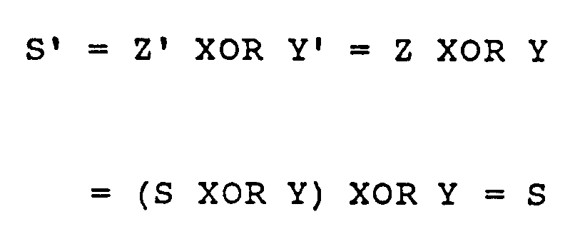
gate 8 with the decoding signal Y' to generate a reproduced signal S'. - The prior art receiving system makes use of a general property of binary digits A and B that

That is, if A and B are any two bits that have been combined by an XOR (Exclusive OR) operation, the way to recover A from the output of the operation is to further XOR the output with B. - Therefore, to enable the digital signal S input to the transmitting system to be reproduced by the receiving system, the prestored random bits of the
receiver memory unit 7 of the receiving system are made identical to those stored in the corresponding addresses of the transmitter memory unit 1 of the transmitting system. - The transmitting system sends the signal


mod 2 addition of the binary signals S and Y. When the signal Z is transmitted without error,

registers 3 and 6 are also equal. That is, the register bits used in parallel for the memory addresses are the same at the receiving end as at the transmitting end,


memory units 7 and 1 are identical, their corresponding outputs Y', Y will also be identical. - It follows that:

That is, reproduced signal S' equals the initial input signal S. - In this prior art system, the encryption and decryption operations are controlled by the particular random bit pattern stored in the addresses in memory units 1 and 6. This important controlling bit pattern is called the encryption key variable.
- Such conventional encryption/decryption devices have the advantages of simple construction and, because they use nonlinear encryption, an exceptionally high level of message secrecy. However, they have the disadvantage that increasing the number of possible random bit patterns that might be stored in the
memories 1 and 7, that is enabling the encryption key variable to have a larger variety of possible values, also increases the system's weakness with respect to transmission errors. For example, in order to increase the variety of random binary bit patterns available for thememories 1 and 7, it is necessary to increase the number of addresses in these memories. Conventionally, the number of bits M used inshift registers 3 and 6 must be increased to add more addresses. - However, increasing the shift register length M can degrade system recovery from transmission errors in the received signal Z'. Until any errors in received signal Z' have passed completely through the M bit shift register 6, they generate errors in the decoding signal Y' output by
memory 7. When these errors are being generated, the output signal S' of the receiving system cannot reproduce the proper transmitted information. This blackout or interruption continues for an interval equal to the time it takes to transmit M bits. - Therefore, these systems have the disadvantage that the number of possible values for the encryption key variable cannot be increased without lengthening the duration of the interrupting effect on the reproduced signal S' caused by any transmission error.
- Fig. 1 shows a block diagram of a first embodiment of an encryption system that overcomes these problems for use at the transmitting end of a communications link. An XOR (Exclusive OR)
gate 10 combines an input digital signal S with a randomized coding signal Y to produce an encrypted digital signal Z. - As part of the encryption, a
shift register 12 receives and temporarily stores the successive bits of signal Z as register bits r₁, r₂, ..., rm. The m register bits are then provided in parallel as an input memory address to atransmitter memory unit 22. Each of the 2m addresses inmemory unit 22 is prestored with a corresponding n bit random number x₁, x₂, ..., xn. - The number n is an integer equal to or greater than 2. As each address r₁, r₂, ..., rm is input,
encoder memory 22 outputs its corresponding stored random number x₁, x₂, ..., xn.Random selection circuit 11 selects from among the n bit random number data x₁, x₂, ..., xn output bymemory unit 22 to form each frame of bits of the coding signal Y. -
Random selection circuit 11 comprises an encoder frame counter 15, anencoder memory 14, and anencoder selector circuit 13. A frame pulse FP output by a framesync pulse generator 16 is input as a clock signal to counter 15, which has q bits. The counter bits b₁, b₂, ..., bq are provided in parallel as an input memory address to theencoder memory 14. Each of the 2q addresses inencoder memory 14 is prestored with a corresponding p bit random number a₁, a₂, ..., ap. The random number a₁, a₂, ..., ap stored at address b₁, b₂, ..., bq is output toselector circuit 13 to change its selection contents. - In other words, encoder counter 15 and
encoder memory 14 together form a random number generator, generating a random number for theselector circuit 13 for each frame of the signal. If desired, a PN (pseudorandom noise) signal generator or the like can instead be used as the random number generator. - Encoding
circuit 13 receives each of the n bit random numbers x₁, x₂, ..., xn output bytransmitter memory unit 22. Based on the value of random number a₁, a₂, ..., ap for the current frame,random selection circuit 13 selects from among the n bit random number data x₁, x₂, ..., xn output bymemory unit 22 to form each frame of bits of the coding signal Y. Signal Y is then combined with input signal S byXOR gate 10 to produce the encrypted digital signal Z. - The encrypted signal Z is input to a
frame composing circuit 19, which combines it with a frame sync signal FS and a START signal prefix to produce a TDATA signal for transmission. The frame sync signal FS is generated by a framesync signal generator 17 in response to a frame sync pulse FP frompulse generator 16. The START signal prefix is generated by astart signal generator 18 in response to the closing of atransmission switch 21. The TDATA signal is then transmitted by atransmitter 20. -
Transmission switch 21 is arranged so that, when it is closed, it activatestransmitter 20. Whenswitch 21 is first closed, it also sends encoder counter 15 a Clear signal to set it to a preselected initial value. - Figure 3 shows the make-up of each frame of the TDATA signal output as well as its relationship in time to its corresponding frame sync pulse. In Fig. 3, "START" indicates the START signal, "FS" the frame sync signal, "Z" the encrypted signal Z, and "FP" the frame sync pulse.
- Figure 2 shows a block diagram of a first embodiment of a decryption system for receiving the signal transmitted by the system of Fig. 1 and reproducing from it the input digital signal S.
- A
receiver 23 picks up the transmitted signal of Fig. 3 and outputs a received digital signal RDATA. Signal RDATA is input to aseparator circuit 24, a framesync signal detector 25, and startsignal detector 26. -
Separator circuit 24 separates out a received encrypted signal Z' from the received signal RDATA. If there have been no errors in the transmission path, this signal Z' is identical to the transmitted encrypted digital signal Z. - More particularly,
detector 26 detects the START signal prefix at the beginning of the RDATA signal and outputs a start pulse SP. Framesync signal detector 25 detects each frame signal FS and outputs a frame sync pulse FP. The frame pulses FP output bydetector 25 are used to synchronize separatingcircuit 24 so that for each frame it can separate out just the signal Z' which corresponds to the Z portion of the transmitted signal of Fig. 3. - The frame pulse FP is also provided as a clock signal to a
decoder frame counter 31 in a decoderrandom selection circuit 28. The start pulse SP fromdetector 26 is provided as a Clear signal to counter 31 to set it to a preselected initial value. - The encrypted received signal Z' output by
circuit 24 is input to both ashift register 27 and anXOR gate 33.Shift register 27 receives and temporarily stores the successive bits of signal Z' as register bits r'₁, r'₂, ..., r'm. These m register bits are then provided in parallel as an input memory address to areceiver memory unit 32. - Each of the 2m addresses in
memory unit 32 is prestored with a corresponding n bit random number x'₁, x'₂, ..., x'n. As each address r'₁, r'₂, ..., r'm is input, the random number x'₁, x'₂, ..., x'n stored at that address is output. Adecoder selector circuit 29 inrandom selection circuit 28 receives and selects from among the n bit random number data x'₁, x'₂, ..., x'n output bymemory unit 32 to form each frame of bits of a decoding signal Y'. Signal Y' is then provided to theXOR gate 33. - Decoder
random selection circuit 28 works exactly like the encoderrandom selection circuit 11 in the encryption system at the transmitting end.Decoder counter 31 is initialized by a start pulse SP fromdetector 26 before counting the frame sync pulses FP output bydetector 25. The output b'₁, b'₂, ..., b'q ofcounter 31 is provided in parallel as address input to a decoder memory 30 for each frame. This outputs a stored random number a'₁, a'₂, ..., a'p for each address. The random number output a'₁, a'₂, ..., a'p controls the selection contents ofdecoder selector circuit 29 for each frame. - Based on the value of random number a'₁, a'₂, ..., a'p for the current frame,
random selection circuit 29 selects from among the n bit random number data x'₁, x'₂, ..., x'n output bymemory unit 32 to form each frame of bits of the decoding signal Y' forXOR gate 33. TheXOR gate 33 then combines encrypted received signal Z' with decoding signal Y' to reproduce digital signal S' as the decrypted message signal. - Counter 15 at the transmitting end and counter 31 at the receiving end are each set to the same preselected initial value before they begin counting frame sync pulses. Decoder memory 30 is prestored with the same pattern of random numbers prestored in
encoder memory 14. This enables decoderrandom selection circuit 28 to follow the identical selection routine employed by encoderrandom selection circuit 11. -
Receiver memory unit 32 is prestored with the same pattern of random numbers prestored intransmitter memory unit 22. Therefore, when there are no transmission errors, the reproduced digital signal S' at the receiver end is identical to the digital signal S input at the transmitting end. For no transmission errors, this result is just as in the prior art encoder/decoder system. - The logical working of the decoding mechanism is as follows. When no errors are introduced by the transmission path, the received signal Z' equals the encrypted cipher signal Z. Then shift
registers memory units receiver memory unit 32 is identical to the random number x₁, x₂, ..., xn previously output bytransmitter memory unit 22. - Since the contents of decoder memory 30 are identical to those of
encoder memory 14, decoderrandom selection circuit 28 can duplicate the working of encoderrandom selection circuit 11. This enables randomized signal Y' to be identical to randomized signal Y. - It follows that:

In the above embodiment not just the contents ofmemory units memories 14 and 30 are also used. Therefore, the amount of random numbers stored inmemory units memory units art memory units 1 and 7 of Figs. 4 and 5. - This enables shift registers 12, 27 to have only m bits, where m is less than the usual M bits used in prior
art shift registers 3 and 6 of Figs. 4 and 5. If an error is generated in the transmission path, it causes errors in the decoding signal Y' for a time interval equal to the time it takes to transmit m bits. However, because the number of bits m inregister 27 can be less than the usual M bits, the amount of time that the received signal S' is not properly reproduced is reduced. - Moreover, the number of bits n stored at each memory address can be selected to be a relatively small number as compared to the address length m, reducing the complexity of
encoder selector circuit 13 anddecoder selector circuit 29. - To the extent that the frame sync signal remains reliable, the variety of random numbers stored in the
encoder memory 14 and decoder memory 30 can be made very large. This effectively gives the encryption key variable a large number of possible values without increasing the errors in decoding signal Y' or the reproduced digital signal S'. - The present invention not only randomizes individual signal bits in the transmitted signal but also changes the selection rule used by encoder
random selection circuit 11 to form encoding signal Y for each frame of the message. This ensures an exceptionally strong level of message secrecy without greatly increasing the errors in reproduced digital signal S'. The number of different values for the encryption key variable of the coder/encoder is greatly increased without sacrificing the system's prompt recovery from any transmission channel errors. - In the encryption system of Fig. 1, a cipher feedback loop comprising, in order, a register (12), a transmitter memory unit (22), and a random selection circuit (11) provides the randomized coding signal Y. Similarly, in the decryption system of Fig. 2, the decoding signal Y' is provided by a cipher feedback loop comprising, in order, a register (27), a transmitter memory unit (32), and a random selection circuit (28).
- Fig. 6 shows a second embodiment of the inventive encryption system having a different cipher feedback loop comprising, in order, a
shift register 12, arandom selection circuit 41, and atransmitter memory unit 42. The remaining portions of the second embodiment of the encryption system are identical to those shown in Fig. 1 for the first embodiment, as indicated by use of identical reference numerals. - More particularly,
shift register 12 stores and outputs in parallel a predetermined number of bits m of the encrypted signal Z output from theXOR gate 10. For each signal frame,random selection circuit 41 randomly selects from among the m bit number data output byshift register 12 and outputs corresponding n bit address numbers w₁, w₂, ..., wn, where n is an integer equal to or greater than 2. -
Transmitter memory unit 42 receives the n bit addresses and for each address w₁, w₂, ..., wn outputs a corresponding random bit prestored at the address. The successive bits output bymemory unit 42 make up the randomized coding signal Y. -
Random selection circuit 41 has aframe counter 45 fed by frame sync pulses FP from a framesync pulse generator 16. The output offrame counter 45 is a q bit number b₁, b₂ ..., bq for each frame. Anencoder memory 44 receives the q bit output ofcounter 45 as an address. It outputs a p bit random number a₁, a₂, ..., ap prestored at that address to aselector circuit 43 which executes the selection made byselection circuit 41. The selection rule ofselector circuit 43 is controlled by the value of random number a₁, a₂, ..., ap for the current frame. In effect, counter 45 andencoder memory 44 generate a p bit random number a₁, a₂, ..., ap for each frame for controllingselector circuit 43. - As the remaining portions of the second embodiment of the encryption system function like those shown in Fig. 1 for the first embodiment, their operation will not again be described.
- Fig. 7 shows a second embodiment of the inventive decryption system for use at the receiving end of a communications link to decode signals transmitted by the system of Fig. 6. This decryption system has a cipher feedback loop comprising, in order, a
shift register 27, arandom selection circuit 58, and a receiver memory unit 52. The remaining portions of the second embodiment of the decryption system are identical to those shown in Fig. 2 for the first embodiment, as indicated by use of identical numerals. - More particularly,
shift register 27 stores and outputs in parallel a predetermined number of bits m of the received encrypted signal Z' output from separatingcircuit 24. For each signal frame, theselection circuit 58 selects from among the m bit number data output byshift register 27 and outputs corresponding n bit address numbers w'₁, w'₂, ..., w'n. - Receiver memory unit 52 has stored contents identical to that of transmitter memory unit 42 (Fig. 6). Memory unit 52 receives the n bit addresses and for each address w'₁, w'₂, ..., w'n outputs a corresponding random bit (0 or 1) prestored at the address. The successive bits output by memory unit 52 make up the decoding signal Y'.
-
Selection circuit 58 operates the same way asrandom selection circuit 41 and in sync with a corresponding frame of the encryptedsignal Z. Circuit 58 has aframe counter 51 fed by frame sync pulses from a framesync signal detector 25. The output offrame counter 51 is a q bit number b'₁, b'₂ ..., b'q for each frame. Adecoder memory 50 has stored contents identical to that of encoder memory 44 (Fig. 6). -
Decoder memory 50 receives the q bit output ofcounter 51 as an address. It outputs a p bit number a'₁, a'₂, ..., a'p prestored at that address to aselector circuit 59 which executes the selection made byselection circuit 58. The selection rule ofselector circuit 59 is controlled by the value of random number a'₁, a'₂, ..., a'p for the current frame. In effect, counter 51 anddecoder memory 50 generate a p bit number a'₁, a'₂ .., a'p for each frame for controllingselector circuit 59. - Since the remaining portions of the second embodiment of the decryption system function like those shown in Fig. 2 for the first embodiment, their working will not again be described. The stored contents and working of the decryption system are chosen to replicate those of the encryption system. When there are no transmission errors the received encrypted signal Z' equals the encrypted signal Z, and the decoding signal Y' equals the randomized encoding signal Y.
- Therefore, when there are no transmission errors the signal S' reproduced by the second embodiment of the decryption system equals the signal S input to the companion encryption system:
As in the first embodiment, the second embodiment of the encryption and decryption systems enables the number of values for the encryption key variable to be increased without increasing the number of bits m used in the shift registers 12 and 27. Instead, the additional randomizing key information is provided in the encrypter by the working ofselector circuit 43,transmitter memory 42,encoder memory 44, andframe counter 45, and their counterparts in the decryption system. - Moreover, the number of bits n in address numbers w₁, w₂, ..., wn and w'₁, w'₂, ..., w'n can be selected to be a relatively small number as compared to the address length m, reducing the complexity of
transmitter memory unit 42 and receiver memory unit 52. - Although the invention has been described, by way of example, with reference to particular examples, it will be understood that variations and modifications may be made within the scope of the appended claims.
- For example, an address may be incremented by means of frame sync signals, the intervals between which may constitute an information data word.
- It will be noted that, in the particular embodiments described, not just the contents of the
memory units memories 14 and 30 may also be used. It is possible to use a randomly cross wired transmitter and receiver memory unit at the opposite ends of the communciation channel to provide randomly changing parameters.
Claims (2)
- An encryption/decryption system for encrypting a digital signal input at the transmitting end of a communications channel and for reproducing the input signal at the receiving end of the channel, including at the transmitting end a first register (12) for storing a predetermined number of bits m of an encrypted signal, and for outputting a plurality of the stored bits in parallel, a first memory (22) for receiving the output from the first register (12) as an address input and for outputting a corresponding prestored n bit random number for each of the various input addresses and means (11) for generating a randomized coding signal to be combined with the input digital signal to form an encrypted signal, and at the receiving end a second register memory (32) for receiving the output from the second register (27) means as an address input and for outputting a corresponding prestored n bit random number for each of the various input addresses, the stored contents of the first (22) and second (32) memories being identical, and means (33) for combining the received encrypted signal with a decoding signal to reproduce the digital signal input at the transmitting end, characterised in that at the transmitting end, the generating means (11) includes a first random number generator (14, 15, 16) for locally generating a first random number for each frame, and a first selector (13) for randomly selecting, based on the first random number from said first random number generator (14, 15, 16), an output from among the n bit random number data output by the first memory (22), where n is an integer which is at least 2, to form each frame of bits of the randomized coding signal, and in that at the receiving end there are a second random number generator (25, 30, 31) for locally generating a second random number for each frame in synchronism with a corresponding frame of the encrypted signal, and a second selector (29), operating in a similar way to the first selector (13), for selecting, based on the second random number from said second random number generator (25, 30, 31), an output from the random number data output from the second memory (32) to provide the decoding signal by forming a frame of bits in synchronism with a corresponding frame of the encrypted signal.
- An encryption/decryption system for encrypting a digital signal input at the transmitting end of a communications channel and for reproducing the input signal at the receiving end of the channel, the system including at the transmitting end a first register (12) for storing a predetermined number of bits m of an encrypted signal and for outputting a plurality of the stored bits in parallel, a first memory (42) for storing and outputting the bits of a randomized coding signal responsive to the receipt of an n bit address number, and means (10) for combining the randomized coding signal with the input digital signal to form an encrypted signal and at the receiving end a second register (27) for storing m bits of a received encrypted signal and for outputting a plurality of the stored bits in parallel, a second memory (52), having stored therein contents which are identical to the contents stored in the first memory (42), and means (33) for combining the received encrypted signal with the decoding signal to reproduce the input digital signal, characterised in that there are provided at the transmitting end a first random number generator (16, 44, 45) for locally generating a first random number for each frame, and a first selector (43) for randomly selecting an output, based on the first random number from said first random number generator (16, 44, 45), for each signal frame, and responsive to the m bit number data output by the first register (12) and for outputting said n bit address number, where n is an integer which is at least 2, and at the receiving end a second random number generator (25, 50, 51) for locally generating a second random number for each frame in synchronism with a corresponding frame of the encrypted signal, and a second selector (59), operating in a similar way to the first selector (43) and in synchronism with the corresponding frame of the encrypted signal, for selecting an output, based on the second random number from said second random number generator (25, 50, 51), and responsive to the m bit number data output by the second register (27) and outputting corresponding n bit address numbers, the second memory (52) producing a prestored decoding signal responsive to the receipt of the n bit addresses output from the second selector (59).
Applications Claiming Priority (4)
| Application Number | Priority Date | Filing Date | Title |
|---|---|---|---|
| JP60268321A JPH0628354B2 (en) | 1985-11-30 | 1985-11-30 | Encryption device |
| JP268321/85 | 1985-11-30 | ||
| JP60268322A JPH0630495B2 (en) | 1985-11-30 | 1985-11-30 | Encryption device |
| JP268322/85 | 1985-11-30 |
Publications (3)
| Publication Number | Publication Date |
|---|---|
| EP0227318A2 EP0227318A2 (en) | 1987-07-01 |
| EP0227318A3 EP0227318A3 (en) | 1989-02-22 |
| EP0227318B1 true EP0227318B1 (en) | 1993-07-07 |
Family
ID=26548266
Family Applications (1)
| Application Number | Title | Priority Date | Filing Date |
|---|---|---|---|
| EP86309231A Expired - Lifetime EP0227318B1 (en) | 1985-11-30 | 1986-11-26 | Encryption/decryption system |
Country Status (5)
| Country | Link |
|---|---|
| US (1) | US4791669A (en) |
| EP (1) | EP0227318B1 (en) |
| AU (1) | AU589080B2 (en) |
| CA (1) | CA1258305A (en) |
| DE (1) | DE3688676T2 (en) |
Cited By (1)
| Publication number | Priority date | Publication date | Assignee | Title |
|---|---|---|---|---|
| RU2502201C2 (en) * | 2006-09-01 | 2013-12-20 | Сони Корпорейшн | Encryption/decryption device, encryption/decryption method, information processing device and computer programme |
Families Citing this family (36)
| Publication number | Priority date | Publication date | Assignee | Title |
|---|---|---|---|---|
| US5261070A (en) * | 1986-07-24 | 1993-11-09 | Meiji Milk Product Co., Ltd. | Method and apparatus for forming unique user identification data at remote terminal for secure transmission of data from host terminal |
| US4969188A (en) * | 1987-02-17 | 1990-11-06 | Gretag Aktiengesellschaft | Process and apparatus for the protection of secret elements in a network of encrypting devices with open key management |
| US5113444A (en) * | 1990-09-05 | 1992-05-12 | Arnold Vobach | Random choice cipher system and method |
| JP2862030B2 (en) * | 1991-06-13 | 1999-02-24 | 三菱電機株式会社 | Encryption method |
| US5199074A (en) * | 1992-01-06 | 1993-03-30 | Advanced Micro Devices, Inc. | Encryption system |
| US5307412A (en) * | 1992-09-30 | 1994-04-26 | Vobach Arnold R | Random coding cipher system and method |
| US5335280A (en) * | 1993-01-28 | 1994-08-02 | Vobach Arnold R | Random sum cipher system and method |
| NL9400428A (en) * | 1994-03-18 | 1995-11-01 | Nederland Ptt | Device for cryptographically processing data packets, as well as a method of generating cryptographic processing data. |
| SE506619C2 (en) * | 1995-09-27 | 1998-01-19 | Ericsson Telefon Ab L M | Method for encrypting information |
| US5859912A (en) * | 1996-03-22 | 1999-01-12 | General Electric Company | Digital information privacy system |
| JPH10301492A (en) | 1997-04-23 | 1998-11-13 | Sony Corp | Enciphering device and method therefor, decoding device and method therefor, and information processing device and method therefor |
| JP4456185B2 (en) * | 1997-08-29 | 2010-04-28 | 富士通株式会社 | Visible watermarked video recording medium with copy protection function and its creation / detection and recording / playback device |
| SG117471A1 (en) * | 2000-01-14 | 2005-12-29 | Mitsubishi Electric Corp | Method and apparatus for encryption, method and apparatus for decryption, and computer-readable med ium storing program |
| US6931128B2 (en) * | 2001-01-16 | 2005-08-16 | Microsoft Corporation | Methods and systems for generating encryption keys using random bit generators |
| US8121292B2 (en) * | 2002-02-26 | 2012-02-21 | Qualcomm Incorporated | Method and apparatus for scrambling information bits on a channel in a communications system |
| JP4199477B2 (en) * | 2002-04-17 | 2008-12-17 | パナソニック株式会社 | Digital bidirectional communication control apparatus and method |
| JP3661663B2 (en) * | 2002-04-19 | 2005-06-15 | 日本電気株式会社 | Random number generation device, random number generation method, random number generation program, audio decoding device and decoding method |
| US20040025039A1 (en) * | 2002-04-30 | 2004-02-05 | Adam Kuenzi | Lock box security system with improved communication |
| US7061367B2 (en) | 2002-04-30 | 2006-06-13 | General Electric Company | Managing access to physical assets |
| CN100521599C (en) * | 2002-08-08 | 2009-07-29 | 松下电器产业株式会社 | Encrypting/decrypting device, encrypting device and decrypting device |
| US8171567B1 (en) | 2002-09-04 | 2012-05-01 | Tracer Detection Technology Corp. | Authentication method and system |
| CN100428666C (en) * | 2002-12-16 | 2008-10-22 | 中国电子科技集团公司第三十研究所 | Cipher-chip key rapid-changing method |
| DE602005014755D1 (en) | 2004-03-12 | 2009-07-16 | Ingenia Technology Ltd | METHOD AND DEVICES FOR PRODUCING AUTHENTICABLE OBJECTS AND THEIR SUBSEQUENT REVIEW |
| EP2131310A3 (en) * | 2004-03-12 | 2011-01-26 | Ingenia Technology Limited | Authenticity of security articles |
| JP2006023957A (en) * | 2004-07-07 | 2006-01-26 | Sony Corp | Semiconductor integrated circuit and information processor |
| GB2438424B (en) * | 2004-08-13 | 2008-02-13 | Ingenia Technology Ltd | Article manufacturing screen |
| GB2417592B (en) | 2004-08-13 | 2006-07-26 | Ingenia Technology Ltd | Authenticity verification of articles |
| US7458008B2 (en) * | 2004-12-30 | 2008-11-25 | Freescale Semiconductor, Inc. | Decision voting in a parallel decoder |
| US7764792B1 (en) * | 2005-01-13 | 2010-07-27 | Marvell International Ltd. | System and method for encoding data transmitted on a bus |
| KR101223204B1 (en) * | 2005-07-27 | 2013-01-17 | 인제니아 홀딩스 리미티드 | Verification of authenticity |
| JP2009521039A (en) | 2005-12-23 | 2009-05-28 | インジェニア・ホールディングス・(ユー・ケイ)・リミテッド | Optical authentication |
| US9670694B2 (en) | 2007-04-12 | 2017-06-06 | Utc Fire & Security Americas Corporation, Inc. | Restricted range lockbox, access device and methods |
| US8233622B2 (en) * | 2008-06-18 | 2012-07-31 | International Business Machines Corporation | Transmitting parallel data via high-speed serial interconnection |
| GB2466311B (en) | 2008-12-19 | 2010-11-03 | Ingenia Holdings | Self-calibration of a matching algorithm for determining authenticity |
| GB2466465B (en) | 2008-12-19 | 2011-02-16 | Ingenia Holdings | Authentication |
| GB2476226B (en) | 2009-11-10 | 2012-03-28 | Ingenia Holdings Ltd | Optimisation |
Family Cites Families (21)
| Publication number | Priority date | Publication date | Assignee | Title |
|---|---|---|---|---|
| US3614316A (en) * | 1964-05-20 | 1971-10-19 | Us Navy | Secure communication system |
| CH411030A (en) * | 1964-08-06 | 1966-04-15 | Patelhold Patentverwertung | Device for encrypting a pulse-shaped message |
| CH516854A (en) * | 1969-11-29 | 1971-12-15 | Ciba Geigy Ag | Method and device for encrypted transmission of information |
| CH530742A (en) * | 1970-08-24 | 1972-11-15 | Ciba Geigy Ag | Device for generating key pulse sequences |
| US3852534A (en) * | 1973-06-07 | 1974-12-03 | Us Army | Method and apparatus for synchronizing pseudorandom coded data sequences |
| US4176247A (en) * | 1973-10-10 | 1979-11-27 | Sperry Rand Corporation | Signal scrambler-unscrambler for binary coded transmission system |
| SE380696B (en) * | 1974-03-20 | 1975-11-10 | Philips Svenska Ab | WAY TO CREATE A PSEUDOS RANDOM BIT SEQUENCE AND DEVICE FOR PERFORMING THE SET. |
| SE385644B (en) * | 1974-10-17 | 1976-07-12 | Ericsson Telefon Ab L M | DEVICE FOR ENCRYPTING AND DECryptING MESSAGES |
| US3950616A (en) * | 1975-04-08 | 1976-04-13 | Bell Telephone Laboratories, Incorporated | Alignment of bytes in a digital data bit stream |
| US4133974A (en) * | 1976-11-05 | 1979-01-09 | Datotek, Inc. | System for locally enciphering prime data |
| DE2706421C2 (en) * | 1977-02-16 | 1979-03-15 | Licentia Patent-Verwaltungs-Gmbh, 6000 Frankfurt | Procedure for setting ciphertext generators in encryption devices |
| US4172213A (en) * | 1977-11-17 | 1979-10-23 | Burroughs Corporation | Byte stream selective encryption/decryption device |
| JPS54129901A (en) * | 1978-03-31 | 1979-10-08 | Toshiba Corp | Secret communication system |
| NL183862C (en) * | 1980-02-04 | 1989-02-01 | Philips Nv | TELECOMMUNICATIONS SYSTEM WITH CODED MESSAGE TRANSMISSION. |
| US4447672A (en) * | 1980-10-06 | 1984-05-08 | Nippon Electric Co., Ltd. | Device for encrypting each input data bit by at least one keying bit decided by a code pattern and a bit pattern of a predetermined number of preceding encrypted bits |
| US4450321A (en) * | 1981-12-08 | 1984-05-22 | Quigley William D | Circuit for producing noise generation for sound masking |
| JPS6020660A (en) * | 1983-07-14 | 1985-02-01 | Sharp Corp | System for randamizing coded information |
| GB2151886A (en) * | 1983-12-21 | 1985-07-24 | British Broadcasting Corp | Conditional-access broadcast transmission |
| GB2154108B (en) * | 1984-02-07 | 1987-06-03 | Communications Patents Ltd | Broadcasting system |
| US4596898A (en) * | 1984-03-14 | 1986-06-24 | Computer Security Systems, Inc. | Method and apparatus for protecting stored and transmitted data from compromise or interception |
| AU580769B2 (en) * | 1984-05-05 | 1989-02-02 | British Encryption Technology Limited | Communications system |
-
1986
- 1986-11-24 US US06/934,408 patent/US4791669A/en not_active Expired - Lifetime
- 1986-11-26 DE DE86309231T patent/DE3688676T2/en not_active Expired - Fee Related
- 1986-11-26 EP EP86309231A patent/EP0227318B1/en not_active Expired - Lifetime
- 1986-11-27 CA CA000523939A patent/CA1258305A/en not_active Expired
- 1986-11-28 AU AU65808/86A patent/AU589080B2/en not_active Ceased
Cited By (1)
| Publication number | Priority date | Publication date | Assignee | Title |
|---|---|---|---|---|
| RU2502201C2 (en) * | 2006-09-01 | 2013-12-20 | Сони Корпорейшн | Encryption/decryption device, encryption/decryption method, information processing device and computer programme |
Also Published As
| Publication number | Publication date |
|---|---|
| EP0227318A2 (en) | 1987-07-01 |
| CA1258305A (en) | 1989-08-08 |
| EP0227318A3 (en) | 1989-02-22 |
| DE3688676T2 (en) | 1993-11-04 |
| AU589080B2 (en) | 1989-09-28 |
| US4791669A (en) | 1988-12-13 |
| AU6580886A (en) | 1987-06-04 |
| DE3688676D1 (en) | 1993-08-12 |
Similar Documents
| Publication | Publication Date | Title |
|---|---|---|
| EP0227318B1 (en) | Encryption/decryption system | |
| US5193115A (en) | Pseudo-random choice cipher and method | |
| US5253294A (en) | Secure transmission system | |
| US5363447A (en) | Method for loading encryption keys into secure transmission devices | |
| US4211891A (en) | Method for setting code text generators in ciphering devices | |
| US6014446A (en) | Apparatus for providing improved encryption protection in a communication system | |
| KR100657062B1 (en) | Method for encrypting information and device for realization of the method | |
| US6069954A (en) | Cryptographic data integrity with serial bit processing and pseudo-random generators | |
| US5703948A (en) | Protected communication method and system | |
| US5444781A (en) | Method and apparatus for decryption using cache storage | |
| EP1094634B1 (en) | Automatic resynchronization of crypto-sync information | |
| US5335280A (en) | Random sum cipher system and method | |
| DK170266B1 (en) | Encryption system and method for encryption and decryption | |
| WO2012140144A1 (en) | Method and system for improving the synchronization of stream ciphers | |
| US4856063A (en) | No-overhead synchronization for cryptographic systems | |
| KR100797106B1 (en) | Method for encrypting and decrypting transmmited and received packet in wireless lan | |
| US4724541A (en) | Data-dependent binary encoder/decoder | |
| WO1985000259A1 (en) | Probabilistic scrambler and method of probabilistic scrambling | |
| JPH06342257A (en) | Sequential ciphering system | |
| JP2003032244A (en) | Stream cipher apparatus | |
| KR100226867B1 (en) | Stream cipher system of wireless communication | |
| JPH04335730A (en) | Random ciphering communication system | |
| EP0619659A2 (en) | A shrinking generator for cryptosystems | |
| EP0035048A1 (en) | Cipher system using a variant key matrix | |
| KR0176080B1 (en) | Method of data coding for conditional access system in digital broadcasting system |
Legal Events
| Date | Code | Title | Description |
|---|---|---|---|
| PUAI | Public reference made under article 153(3) epc to a published international application that has entered the european phase |
Free format text: ORIGINAL CODE: 0009012 |
|
| 17P | Request for examination filed |
Effective date: 19861219 |
|
| AK | Designated contracting states |
Kind code of ref document: A2 Designated state(s): DE FR GB NL SE |
|
| PUAL | Search report despatched |
Free format text: ORIGINAL CODE: 0009013 |
|
| AK | Designated contracting states |
Kind code of ref document: A3 Designated state(s): DE FR GB NL SE |
|
| 17Q | First examination report despatched |
Effective date: 19910423 |
|
| GRAA | (expected) grant |
Free format text: ORIGINAL CODE: 0009210 |
|
| AK | Designated contracting states |
Kind code of ref document: B1 Designated state(s): DE FR GB NL SE |
|
| PG25 | Lapsed in a contracting state [announced via postgrant information from national office to epo] |
Ref country code: NL Effective date: 19930707 |
|
| REF | Corresponds to: |
Ref document number: 3688676 Country of ref document: DE Date of ref document: 19930812 |
|
| ET | Fr: translation filed | ||
| NLV1 | Nl: lapsed or annulled due to failure to fulfill the requirements of art. 29p and 29m of the patents act | ||
| PLBE | No opposition filed within time limit |
Free format text: ORIGINAL CODE: 0009261 |
|
| STAA | Information on the status of an ep patent application or granted ep patent |
Free format text: STATUS: NO OPPOSITION FILED WITHIN TIME LIMIT |
|
| 26N | No opposition filed | ||
| EAL | Se: european patent in force in sweden |
Ref document number: 86309231.8 |
|
| PGFP | Annual fee paid to national office [announced via postgrant information from national office to epo] |
Ref country code: GB Payment date: 19971107 Year of fee payment: 12 |
|
| PGFP | Annual fee paid to national office [announced via postgrant information from national office to epo] |
Ref country code: SE Payment date: 19971110 Year of fee payment: 12 |
|
| PGFP | Annual fee paid to national office [announced via postgrant information from national office to epo] |
Ref country code: FR Payment date: 19971117 Year of fee payment: 12 |
|
| PGFP | Annual fee paid to national office [announced via postgrant information from national office to epo] |
Ref country code: DE Payment date: 19980130 Year of fee payment: 12 |
|
| PG25 | Lapsed in a contracting state [announced via postgrant information from national office to epo] |
Ref country code: GB Free format text: LAPSE BECAUSE OF NON-PAYMENT OF DUE FEES Effective date: 19981126 |
|
| PG25 | Lapsed in a contracting state [announced via postgrant information from national office to epo] |
Ref country code: SE Free format text: LAPSE BECAUSE OF NON-PAYMENT OF DUE FEES Effective date: 19981127 |
|
| GBPC | Gb: european patent ceased through non-payment of renewal fee |
Effective date: 19981126 |
|
| PG25 | Lapsed in a contracting state [announced via postgrant information from national office to epo] |
Ref country code: FR Free format text: LAPSE BECAUSE OF NON-PAYMENT OF DUE FEES Effective date: 19990730 |
|
| EUG | Se: european patent has lapsed |
Ref document number: 86309231.8 |
|
| REG | Reference to a national code |
Ref country code: FR Ref legal event code: ST |
|
| PG25 | Lapsed in a contracting state [announced via postgrant information from national office to epo] |
Ref country code: DE Free format text: LAPSE BECAUSE OF NON-PAYMENT OF DUE FEES Effective date: 19990901 |