EP0227303A2 - Method of manufacturing semiconductor devices having side-wall isolation - Google Patents
Method of manufacturing semiconductor devices having side-wall isolation Download PDFInfo
- Publication number
- EP0227303A2 EP0227303A2 EP86309083A EP86309083A EP0227303A2 EP 0227303 A2 EP0227303 A2 EP 0227303A2 EP 86309083 A EP86309083 A EP 86309083A EP 86309083 A EP86309083 A EP 86309083A EP 0227303 A2 EP0227303 A2 EP 0227303A2
- Authority
- EP
- European Patent Office
- Prior art keywords
- layer
- sidewall
- oxide
- feature
- polysilicon
- Prior art date
- Legal status (The legal status is an assumption and is not a legal conclusion. Google has not performed a legal analysis and makes no representation as to the accuracy of the status listed.)
- Withdrawn
Links
Images

Classifications
-
- H—ELECTRICITY
- H01—ELECTRIC ELEMENTS
- H01L—SEMICONDUCTOR DEVICES NOT COVERED BY CLASS H10
- H01L21/00—Processes or apparatus adapted for the manufacture or treatment of semiconductor or solid state devices or of parts thereof
- H01L21/02—Manufacture or treatment of semiconductor devices or of parts thereof
- H01L21/04—Manufacture or treatment of semiconductor devices or of parts thereof the devices having at least one potential-jump barrier or surface barrier, e.g. PN junction, depletion layer or carrier concentration layer
- H01L21/18—Manufacture or treatment of semiconductor devices or of parts thereof the devices having at least one potential-jump barrier or surface barrier, e.g. PN junction, depletion layer or carrier concentration layer the devices having semiconductor bodies comprising elements of Group IV of the Periodic System or AIIIBV compounds with or without impurities, e.g. doping materials
- H01L21/30—Treatment of semiconductor bodies using processes or apparatus not provided for in groups H01L21/20 - H01L21/26
- H01L21/31—Treatment of semiconductor bodies using processes or apparatus not provided for in groups H01L21/20 - H01L21/26 to form insulating layers thereon, e.g. for masking or by using photolithographic techniques; After treatment of these layers; Selection of materials for these layers
- H01L21/3205—Deposition of non-insulating-, e.g. conductive- or resistive-, layers on insulating layers; After-treatment of these layers
- H01L21/321—After treatment
-
- H—ELECTRICITY
- H01—ELECTRIC ELEMENTS
- H01L—SEMICONDUCTOR DEVICES NOT COVERED BY CLASS H10
- H01L21/00—Processes or apparatus adapted for the manufacture or treatment of semiconductor or solid state devices or of parts thereof
- H01L21/02—Manufacture or treatment of semiconductor devices or of parts thereof
- H01L21/027—Making masks on semiconductor bodies for further photolithographic processing not provided for in group H01L21/18 or H01L21/34
- H01L21/033—Making masks on semiconductor bodies for further photolithographic processing not provided for in group H01L21/18 or H01L21/34 comprising inorganic layers
- H01L21/0334—Making masks on semiconductor bodies for further photolithographic processing not provided for in group H01L21/18 or H01L21/34 comprising inorganic layers characterised by their size, orientation, disposition, behaviour, shape, in horizontal or vertical plane
- H01L21/0337—Making masks on semiconductor bodies for further photolithographic processing not provided for in group H01L21/18 or H01L21/34 comprising inorganic layers characterised by their size, orientation, disposition, behaviour, shape, in horizontal or vertical plane characterised by the process involved to create the mask, e.g. lift-off masks, sidewalls, or to modify the mask, e.g. pre-treatment, post-treatment
Definitions
- the present invention concerns improvements in or relating to methods of semiconductor device manufacture, in particular methods for manufacturing devices having sidewall isolation.
- Figures l to 3 illustrate steps performed during a typical conventional sidewall isolation method.
- the starting point is a polysilicon/silicon feature l topped with oxide 5 which has been defined using anisotropic etching to achieve near-vertical walls, (Fig.l).
- a sidewall oxide 7 is grown thermally (Fig.2) then etched anisotropically (Fig.3).
- the polysilicon/silicon feature l and the substrate 3 are both oxidised away by an amount at least as thick as the resulting sidewall, and there is significant dopant redistribution in these regions.
- deposited oxide could not ordinarily be used instead because of its poor quality and conformity.
- the anisotropic etch must remove a layer of oxide approximately twice as thick as the sidewall, any overetch causing damage to the underlying substrate. It is also usual that the overall step height is much greater than the final sidewall thickness achieved.
- the present invention provides an alternative method, a method intended to result in significantly less damage to the underlying substrate and to the polysilicon/silicon feature.
- a method of semiconductor device manufacture comprising the following steps:- providing a silicon substrate and forming thereon a feature of either silicon or polysilicon material, this feature being topped by a layer of dielectric; applying to this feature, and to the exposed surface of the silicon substrate, a covering layer of nitride; applying to this covering layer, a layer of polysilicon material; forming an oxide sidewall by a combination of thermal oxidation and anisotropic etching of the polysilicon material; and, removing the exposed layer of nitride.
- the nitride covering layer serves to protect the polysilicon/silicon feature and the substrate during sidewall oxide growth and during the polysilicon anisotropic etch. It also acts as a barrier to interstitial defects generated at the advancing oxidation front and so inhibits enhanced diffusion effects. Thus the polysilicon/silicon feature and substrate are not oxidised during these steps. High pressure oxidation can be used to great advantage to minimise dopant redistribution during the sidewall oxidation.
- the sidewall oxide is of good quality because it is thermally grown.
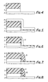
- FIGs 4 to 8 The successive steps performed for this inventive sidewall isolation technique are illustrated in Figures 4 to 8.
- This technique has two novel features.
- a composite nitride-oxide sidewall is produced consisting mainly of good quality thermal oxide l5.
- Figure 4 shows the same starting point as described for the conventional approach.
- Layers of silicon-nitride 9 and polysilicon ll are deposited (Fig.5). Prior to deposition of these layers, however, a thin pad oxide stress relief film may be grown if desired.
- the polysilicon layer ll is etched anisotropically to leave a sidewall fillet l3 (Fig.6) which is then oxidised, (Fig.7).
- the polysilicon may be oxidised first and this oxide etched anisotropically, but this does not have the advantage of the expansion of the polysilicon fillet as it oxidises. Finally the nitride 9 is etched off along with any pad oxide if present (Fig.8).
- the method aforesaid may be used in advanced silicon bipolar processing. It is also possible that it will find application in MOS/CMOS processing.
Abstract
Description
- The present invention concerns improvements in or relating to methods of semiconductor device manufacture, in particular methods for manufacturing devices having sidewall isolation.
- It is common practice in semiconductor manufacture to form dielectric sidewalls on polysilicon or silicon features by means of anisotropic etching of oxide.
- Figures l to 3 illustrate steps performed during a typical conventional sidewall isolation method. The starting point is a polysilicon/silicon feature l topped with
oxide 5 which has been defined using anisotropic etching to achieve near-vertical walls, (Fig.l). Asidewall oxide 7 is grown thermally (Fig.2) then etched anisotropically (Fig.3). - This conventional method has several deleterious consequences. The polysilicon/silicon feature l and the
substrate 3 are both oxidised away by an amount at least as thick as the resulting sidewall, and there is significant dopant redistribution in these regions. Note that deposited oxide could not ordinarily be used instead because of its poor quality and conformity. The anisotropic etch must remove a layer of oxide approximately twice as thick as the sidewall, any overetch causing damage to the underlying substrate. It is also usual that the overall step height is much greater than the final sidewall thickness achieved. - The present invention provides an alternative method, a method intended to result in significantly less damage to the underlying substrate and to the polysilicon/silicon feature.
- In accordance with the present invention there is provided a method of semiconductor device manufacture comprising the following steps:-
providing a silicon substrate and forming thereon a feature of either silicon or polysilicon material, this feature being topped by a layer of dielectric;
applying to this feature, and to the exposed surface of the silicon substrate, a covering layer of nitride;
applying to this covering layer, a layer of polysilicon material;
forming an oxide sidewall by a combination of thermal oxidation and anisotropic etching of the polysilicon material; and,
removing the exposed layer of nitride. - In the method aforesaid it is preferable to form the sidewall oxide by carrying out anisotropic etching prior to thermal oxidation. This preferred sequence has the advantage that the sidewall layer expands upon oxidation and thus forms a thicker structure than would be obtained by the reverse sequence.
- The nitride covering layer serves to protect the polysilicon/silicon feature and the substrate during sidewall oxide growth and during the polysilicon anisotropic etch. It also acts as a barrier to interstitial defects generated at the advancing oxidation front and so inhibits enhanced diffusion effects. Thus the polysilicon/silicon feature and substrate are not oxidised during these steps. High pressure oxidation can be used to great advantage to minimise dopant redistribution during the sidewall oxidation. The sidewall oxide is of good quality because it is thermally grown.
- In the drawings accompanying this specification:-
- Figures l to 3 illustrate in cross-section, a substrate and feature at stages during the growth of a sidewall by a conventional method; and,
- Figures 4 to 8 illustrate in cross-section, the same but where sidewall growth is performed by the method disclosed herein.
- So that the invention may be better understood, embodiments thereof will now be described with reference to the drawings. Such description as follows is given by way of example, only.
- The successive steps performed for this inventive sidewall isolation technique are illustrated in Figures 4 to 8. This technique has two novel features. The use of a protective nitride capping layer 9 and also use of an expanding polysilicon sidewall l3. As a result a composite nitride-oxide sidewall is produced consisting mainly of good quality thermal oxide l5. Figure 4 shows the same starting point as described for the conventional approach. Layers of silicon-nitride 9 and polysilicon ll are deposited (Fig.5). Prior to deposition of these layers, however, a thin pad oxide stress relief film may be grown if desired. The polysilicon layer ll is etched anisotropically to leave a sidewall fillet l3 (Fig.6) which is then oxidised, (Fig.7). Alternatively the polysilicon may be oxidised first and this oxide etched anisotropically, but this does not have the advantage of the expansion of the polysilicon fillet as it oxidises. Finally the nitride 9 is etched off along with any pad oxide if present (Fig.8).
- The method aforesaid may be used in advanced silicon bipolar processing. It is also possible that it will find application in MOS/CMOS processing.
Claims (4)
providing a silicon substrate (3) and forming thereon a feature (l) of either silicon or polysilicon material, this feature (l) being topped by a layer of dielectric (5);
applying to this feature (l), and to the exposed surface of the silicon substrate, a covering layer of nitride (9);
applying to this covering layer (9), a layer (ll) of polysilicon material;
forming an oxide sidewall (l5) by a combination of thermal oxidation and anisotropic etching of the polysilicon material (ll); and,
removing the exposed layer (9) of nitride.
Applications Claiming Priority (2)
| Application Number | Priority Date | Filing Date | Title |
|---|---|---|---|
| GB8528967 | 1985-11-25 | ||
| GB858528967A GB8528967D0 (en) | 1985-11-25 | 1985-11-25 | Semiconductor device manufacture |
Publications (2)
| Publication Number | Publication Date |
|---|---|
| EP0227303A2 true EP0227303A2 (en) | 1987-07-01 |
| EP0227303A3 EP0227303A3 (en) | 1989-11-29 |
Family
ID=10588728
Family Applications (1)
| Application Number | Title | Priority Date | Filing Date |
|---|---|---|---|
| EP86309083A Withdrawn EP0227303A3 (en) | 1985-11-25 | 1986-11-20 | Method of manufacturing semiconductor devices having side-wall isolation |
Country Status (3)
| Country | Link |
|---|---|
| EP (1) | EP0227303A3 (en) |
| JP (1) | JPS62188321A (en) |
| GB (2) | GB8528967D0 (en) |
Cited By (47)
| Publication number | Priority date | Publication date | Assignee | Title |
|---|---|---|---|---|
| EP0237684A2 (en) * | 1986-01-08 | 1987-09-23 | Advanced Micro Devices, Inc. | Production of integrated-circuit devices incorporating a diffusion stop for oxygen |
| EP0265584A2 (en) * | 1986-10-30 | 1988-05-04 | International Business Machines Corporation | Method and materials for etching silicon dioxide using silicon nitride or silicon rich dioxide as an etch barrier |
| US4904612A (en) * | 1987-10-23 | 1990-02-27 | Siemens Aktiengesellschaft | Method for manufacturing a planar, self-aligned emitter-base complex |
| EP0491408A2 (en) * | 1990-11-20 | 1992-06-24 | Consorzio per la Ricerca sulla Microelettronica nel Mezzogiorno - CoRiMMe | Process for making planarized sub-micrometric trenches in integrated circuits |
| EP1164636A2 (en) * | 2000-06-16 | 2001-12-19 | Chartered Semiconductor Manufacturing Pte Ltd. | Method to form self aligned, L-shaped sidewall spacers |
| US6902867B2 (en) | 2002-10-02 | 2005-06-07 | Lexmark International, Inc. | Ink jet printheads and methods therefor |
| US6984015B2 (en) | 2003-08-12 | 2006-01-10 | Lexmark International, Inc. | Ink jet printheads and method therefor |
| WO2006028705A2 (en) * | 2004-09-01 | 2006-03-16 | Micron Technology, Inc. | Mask material conversion |
| US7115525B2 (en) | 2004-09-02 | 2006-10-03 | Micron Technology, Inc. | Method for integrated circuit fabrication using pitch multiplication |
| US7151040B2 (en) | 2004-08-31 | 2006-12-19 | Micron Technology, Inc. | Methods for increasing photo alignment margins |
| US7253118B2 (en) | 2005-03-15 | 2007-08-07 | Micron Technology, Inc. | Pitch reduced patterns relative to photolithography features |
| US7517804B2 (en) | 2006-08-31 | 2009-04-14 | Micron Technologies, Inc. | Selective etch chemistries for forming high aspect ratio features and associated structures |
| US7538858B2 (en) | 2006-01-11 | 2009-05-26 | Micron Technology, Inc. | Photolithographic systems and methods for producing sub-diffraction-limited features |
| US7648919B2 (en) | 2005-03-28 | 2010-01-19 | Tran Luan C | Integrated circuit fabrication |
| US7659208B2 (en) | 2007-12-06 | 2010-02-09 | Micron Technology, Inc | Method for forming high density patterns |
| US7666578B2 (en) | 2006-09-14 | 2010-02-23 | Micron Technology, Inc. | Efficient pitch multiplication process |
| US7687342B2 (en) | 2005-09-01 | 2010-03-30 | Micron Technology, Inc. | Method of manufacturing a memory device |
| US7736980B2 (en) | 2006-03-02 | 2010-06-15 | Micron Technology, Inc. | Vertical gated access transistor |
| US7737039B2 (en) | 2007-11-01 | 2010-06-15 | Micron Technology, Inc. | Spacer process for on pitch contacts and related structures |
| US7790531B2 (en) | 2007-12-18 | 2010-09-07 | Micron Technology, Inc. | Methods for isolating portions of a loop of pitch-multiplied material and related structures |
| US7795149B2 (en) | 2006-06-01 | 2010-09-14 | Micron Technology, Inc. | Masking techniques and contact imprint reticles for dense semiconductor fabrication |
| US7829262B2 (en) | 2005-08-31 | 2010-11-09 | Micron Technology, Inc. | Method of forming pitch multipled contacts |
| US7842558B2 (en) | 2006-03-02 | 2010-11-30 | Micron Technology, Inc. | Masking process for simultaneously patterning separate regions |
| US7888721B2 (en) | 2005-07-06 | 2011-02-15 | Micron Technology, Inc. | Surround gate access transistors with grown ultra-thin bodies |
| US7923373B2 (en) | 2007-06-04 | 2011-04-12 | Micron Technology, Inc. | Pitch multiplication using self-assembling materials |
| US7939409B2 (en) | 2005-09-01 | 2011-05-10 | Micron Technology, Inc. | Peripheral gate stacks and recessed array gates |
| US7977236B2 (en) | 2005-09-01 | 2011-07-12 | Micron Technology, Inc. | Method of forming a transistor gate of a recessed access device, method of forming a recessed transistor gate and a non-recessed transistor gate, and method of fabricating an integrated circuit |
| US8003310B2 (en) | 2006-04-24 | 2011-08-23 | Micron Technology, Inc. | Masking techniques and templates for dense semiconductor fabrication |
| US8003542B2 (en) | 2005-06-02 | 2011-08-23 | Micron Technology, Inc. | Multiple spacer steps for pitch multiplication |
| US8011090B2 (en) | 2005-09-01 | 2011-09-06 | Micron Technology, Inc. | Method for forming and planarizing adjacent regions of an integrated circuit |
| US8030217B2 (en) | 2006-04-07 | 2011-10-04 | Micron Technology, Inc. | Simplified pitch doubling process flow |
| US8043915B2 (en) | 2005-09-01 | 2011-10-25 | Micron Technology, Inc. | Pitch multiplied mask patterns for isolated features |
| US8076208B2 (en) | 2008-07-03 | 2011-12-13 | Micron Technology, Inc. | Method for forming transistor with high breakdown voltage using pitch multiplication technique |
| US8101497B2 (en) | 2008-09-11 | 2012-01-24 | Micron Technology, Inc. | Self-aligned trench formation |
| US8114573B2 (en) | 2006-06-02 | 2012-02-14 | Micron Technology, Inc. | Topography based patterning |
| US8129289B2 (en) | 2006-10-05 | 2012-03-06 | Micron Technology, Inc. | Method to deposit conformal low temperature SiO2 |
| US8207614B2 (en) | 2005-05-23 | 2012-06-26 | Micron Technology, Inc. | Methods for forming arrays of small, closely spaced features |
| US8222105B2 (en) | 2005-08-31 | 2012-07-17 | Micron Technology, Inc. | Methods of fabricating a memory device |
| US8266558B2 (en) | 2005-09-01 | 2012-09-11 | Micron Technology, Inc. | Methods for forming arrays of small, closely spaced features |
| US8264010B2 (en) | 2005-07-29 | 2012-09-11 | Round Rock Research, Llc | Layout for high density conductive interconnects |
| US8334211B2 (en) | 2006-04-25 | 2012-12-18 | Micron Technology, Inc. | Process for improving critical dimension uniformity of integrated circuit arrays |
| US8338085B2 (en) | 2004-09-02 | 2012-12-25 | Micron Technology, Inc. | Method to align mask patterns |
| US8492282B2 (en) | 2008-11-24 | 2013-07-23 | Micron Technology, Inc. | Methods of forming a masking pattern for integrated circuits |
| US8557704B2 (en) | 2006-08-30 | 2013-10-15 | Micron Technology, Inc. | Single spacer process for multiplying pitch by a factor greater than two and related intermediate IC structures |
| US8563229B2 (en) | 2007-07-31 | 2013-10-22 | Micron Technology, Inc. | Process of semiconductor fabrication with mask overlay on pitch multiplied features and associated structures |
| US9048194B2 (en) | 2008-03-21 | 2015-06-02 | Micron Technology, Inc. | Method for selectively modifying spacing between pitch multiplied structures |
| US9099314B2 (en) | 2005-09-01 | 2015-08-04 | Micron Technology, Inc. | Pitch multiplication spacers and methods of forming the same |
Families Citing this family (6)
| Publication number | Priority date | Publication date | Assignee | Title |
|---|---|---|---|---|
| US7390746B2 (en) | 2005-03-15 | 2008-06-24 | Micron Technology, Inc. | Multiple deposition for integration of spacers in pitch multiplication process |
| US7396781B2 (en) | 2005-06-09 | 2008-07-08 | Micron Technology, Inc. | Method and apparatus for adjusting feature size and position |
| US7541632B2 (en) | 2005-06-14 | 2009-06-02 | Micron Technology, Inc. | Relaxed-pitch method of aligning active area to digit line |
| US7768051B2 (en) | 2005-07-25 | 2010-08-03 | Micron Technology, Inc. | DRAM including a vertical surround gate transistor |
| US8123968B2 (en) | 2005-08-25 | 2012-02-28 | Round Rock Research, Llc | Multiple deposition for integration of spacers in pitch multiplication process |
| US7816262B2 (en) | 2005-08-30 | 2010-10-19 | Micron Technology, Inc. | Method and algorithm for random half pitched interconnect layout with constant spacing |
Citations (1)
| Publication number | Priority date | Publication date | Assignee | Title |
|---|---|---|---|---|
| EP0043942A2 (en) * | 1980-07-08 | 1982-01-20 | International Business Machines Corporation | Method for forming integrated circuits having a pattern of narrow dimensioned dielectric regions |
-
1985
- 1985-11-25 GB GB858528967A patent/GB8528967D0/en active Pending
-
1986
- 1986-11-18 GB GB08627568A patent/GB2185351B/en not_active Expired
- 1986-11-20 EP EP86309083A patent/EP0227303A3/en not_active Withdrawn
- 1986-11-25 JP JP28056586A patent/JPS62188321A/en active Pending
Patent Citations (1)
| Publication number | Priority date | Publication date | Assignee | Title |
|---|---|---|---|---|
| EP0043942A2 (en) * | 1980-07-08 | 1982-01-20 | International Business Machines Corporation | Method for forming integrated circuits having a pattern of narrow dimensioned dielectric regions |
Non-Patent Citations (2)
| Title |
|---|
| IBM TECHNICAL DISCLOSURE BULLETIN, vol. 25, no. 11A, April 1983, pages 5727-5728, New York, US; S.A. ABBAS et al.: "Lateral PNP" * |
| IBM TECHNICAL DISCLOSURE BULLETIN, vol. 26, no. 1, June 1983, pages 253-255, New York, US; S.G. BARBEE et al.: "Polysilicon base/emitter contact process" * |
Cited By (115)
| Publication number | Priority date | Publication date | Assignee | Title |
|---|---|---|---|---|
| EP0237684A2 (en) * | 1986-01-08 | 1987-09-23 | Advanced Micro Devices, Inc. | Production of integrated-circuit devices incorporating a diffusion stop for oxygen |
| EP0237684A3 (en) * | 1986-01-08 | 1991-01-09 | Advanced Micro Devices, Inc. | Production of integrated-circuit devices incorporating a diffusion stop for oxygen |
| EP0265584A2 (en) * | 1986-10-30 | 1988-05-04 | International Business Machines Corporation | Method and materials for etching silicon dioxide using silicon nitride or silicon rich dioxide as an etch barrier |
| EP0265584A3 (en) * | 1986-10-30 | 1989-12-06 | International Business Machines Corporation | Method and materials for etching silicon dioxide using silicon nitride or silicon rich dioxide as an etch barrier |
| US4904612A (en) * | 1987-10-23 | 1990-02-27 | Siemens Aktiengesellschaft | Method for manufacturing a planar, self-aligned emitter-base complex |
| EP0491408A3 (en) * | 1990-11-20 | 1992-10-28 | Consorzio Per La Ricerca Sulla Microelettronica Nel Mezzogiorno | Process for making planarized sub-micrometric trenches in integrated circuits |
| EP0491408A2 (en) * | 1990-11-20 | 1992-06-24 | Consorzio per la Ricerca sulla Microelettronica nel Mezzogiorno - CoRiMMe | Process for making planarized sub-micrometric trenches in integrated circuits |
| EP1164636A2 (en) * | 2000-06-16 | 2001-12-19 | Chartered Semiconductor Manufacturing Pte Ltd. | Method to form self aligned, L-shaped sidewall spacers |
| EP1164636A3 (en) * | 2000-06-16 | 2002-12-18 | Chartered Semiconductor Manufacturing Pte Ltd. | Method to form self aligned, L-shaped sidewall spacers |
| US6902867B2 (en) | 2002-10-02 | 2005-06-07 | Lexmark International, Inc. | Ink jet printheads and methods therefor |
| US6984015B2 (en) | 2003-08-12 | 2006-01-10 | Lexmark International, Inc. | Ink jet printheads and method therefor |
| US7151040B2 (en) | 2004-08-31 | 2006-12-19 | Micron Technology, Inc. | Methods for increasing photo alignment margins |
| US8030222B2 (en) | 2004-08-31 | 2011-10-04 | Round Rock Research, Llc | Structures with increased photo-alignment margins |
| US8486610B2 (en) | 2004-09-01 | 2013-07-16 | Micron Technology, Inc. | Mask material conversion |
| US8895232B2 (en) | 2004-09-01 | 2014-11-25 | Micron Technology, Inc. | Mask material conversion |
| WO2006028705A3 (en) * | 2004-09-01 | 2006-04-13 | Micron Technology Inc | Mask material conversion |
| WO2006028705A2 (en) * | 2004-09-01 | 2006-03-16 | Micron Technology, Inc. | Mask material conversion |
| US8216949B2 (en) | 2004-09-02 | 2012-07-10 | Round Rock Research, Llc | Method for integrated circuit fabrication using pitch multiplication |
| US8674512B2 (en) | 2004-09-02 | 2014-03-18 | Micron Technology, Inc. | Method to align mask patterns |
| US8338085B2 (en) | 2004-09-02 | 2012-12-25 | Micron Technology, Inc. | Method to align mask patterns |
| US7115525B2 (en) | 2004-09-02 | 2006-10-03 | Micron Technology, Inc. | Method for integrated circuit fabrication using pitch multiplication |
| US7253118B2 (en) | 2005-03-15 | 2007-08-07 | Micron Technology, Inc. | Pitch reduced patterns relative to photolithography features |
| US8598632B2 (en) | 2005-03-15 | 2013-12-03 | Round Rock Research Llc | Integrated circuit having pitch reduced patterns relative to photoithography features |
| US8048812B2 (en) | 2005-03-15 | 2011-11-01 | Round Rock Research, Llc | Pitch reduced patterns relative to photolithography features |
| US9147608B2 (en) | 2005-03-28 | 2015-09-29 | Micron Technology, Inc. | Integrated circuit fabrication |
| US7776683B2 (en) | 2005-03-28 | 2010-08-17 | Micron Technology, Inc. | Integrated circuit fabrication |
| US8158476B2 (en) | 2005-03-28 | 2012-04-17 | Micron Technology, Inc. | Integrated circuit fabrication |
| US8859362B2 (en) | 2005-03-28 | 2014-10-14 | Micron Technology, Inc. | Integrated circuit fabrication |
| US7648919B2 (en) | 2005-03-28 | 2010-01-19 | Tran Luan C | Integrated circuit fabrication |
| US9412594B2 (en) | 2005-03-28 | 2016-08-09 | Micron Technology, Inc. | Integrated circuit fabrication |
| US8507341B2 (en) | 2005-03-28 | 2013-08-13 | Micron Technology, Inc. | Integrated circuit fabrication |
| US9099402B2 (en) | 2005-05-23 | 2015-08-04 | Micron Technology, Inc. | Integrated circuit structure having arrays of small, closely spaced features |
| US8207614B2 (en) | 2005-05-23 | 2012-06-26 | Micron Technology, Inc. | Methods for forming arrays of small, closely spaced features |
| US8865598B2 (en) | 2005-06-02 | 2014-10-21 | Micron Technology, Inc. | Method for positioning spacers in pitch multiplication |
| US8003542B2 (en) | 2005-06-02 | 2011-08-23 | Micron Technology, Inc. | Multiple spacer steps for pitch multiplication |
| US8598041B2 (en) | 2005-06-02 | 2013-12-03 | Micron Technology, Inc. | Method for positioning spacers in pitch multiplication |
| US9117766B2 (en) | 2005-06-02 | 2015-08-25 | Micron Technology, Inc. | Method for positioning spacers in pitch multiplication |
| US8173550B2 (en) | 2005-06-02 | 2012-05-08 | Micron Technology, Inc. | Method for positioning spacers for pitch multiplication |
| US7888721B2 (en) | 2005-07-06 | 2011-02-15 | Micron Technology, Inc. | Surround gate access transistors with grown ultra-thin bodies |
| US8264010B2 (en) | 2005-07-29 | 2012-09-11 | Round Rock Research, Llc | Layout for high density conductive interconnects |
| US8481385B2 (en) | 2005-08-31 | 2013-07-09 | Micron Technology, Inc. | Methods of fabricating a memory device |
| US8426118B2 (en) | 2005-08-31 | 2013-04-23 | Micron Technology, Inc. | Method of forming pitch multiplied contacts |
| US8546215B2 (en) | 2005-08-31 | 2013-10-01 | Micron Technology, Inc. | Methods of fabricating a memory device |
| US8222105B2 (en) | 2005-08-31 | 2012-07-17 | Micron Technology, Inc. | Methods of fabricating a memory device |
| US7829262B2 (en) | 2005-08-31 | 2010-11-09 | Micron Technology, Inc. | Method of forming pitch multipled contacts |
| US8609324B2 (en) | 2005-08-31 | 2013-12-17 | Micron Technology, Inc. | Method of forming pitch multiplied contacts |
| US8252646B2 (en) | 2005-09-01 | 2012-08-28 | Micron Technology, Inc. | Peripheral gate stacks and recessed array gates |
| US9082829B2 (en) | 2005-09-01 | 2015-07-14 | Micron Technology, Inc. | Methods for forming arrays of small, closely spaced features |
| US10396281B2 (en) | 2005-09-01 | 2019-08-27 | Micron Technology, Inc. | Methods for forming arrays of small, closely spaced features |
| US9679781B2 (en) | 2005-09-01 | 2017-06-13 | Micron Technology, Inc. | Methods for integrated circuit fabrication with protective coating for planarization |
| US9099314B2 (en) | 2005-09-01 | 2015-08-04 | Micron Technology, Inc. | Pitch multiplication spacers and methods of forming the same |
| US9076888B2 (en) | 2005-09-01 | 2015-07-07 | Micron Technology, Inc. | Silicided recessed silicon |
| US9003651B2 (en) | 2005-09-01 | 2015-04-14 | Micron Technology, Inc. | Methods for integrated circuit fabrication with protective coating for planarization |
| US7687342B2 (en) | 2005-09-01 | 2010-03-30 | Micron Technology, Inc. | Method of manufacturing a memory device |
| US8043915B2 (en) | 2005-09-01 | 2011-10-25 | Micron Technology, Inc. | Pitch multiplied mask patterns for isolated features |
| US8601410B2 (en) | 2005-09-01 | 2013-12-03 | Micron Technology, Inc. | Methods for forming arrays of small, closely spaced features |
| US8266558B2 (en) | 2005-09-01 | 2012-09-11 | Micron Technology, Inc. | Methods for forming arrays of small, closely spaced features |
| US7935999B2 (en) | 2005-09-01 | 2011-05-03 | Micron Technology, Inc. | Memory device |
| US7939409B2 (en) | 2005-09-01 | 2011-05-10 | Micron Technology, Inc. | Peripheral gate stacks and recessed array gates |
| US7977236B2 (en) | 2005-09-01 | 2011-07-12 | Micron Technology, Inc. | Method of forming a transistor gate of a recessed access device, method of forming a recessed transistor gate and a non-recessed transistor gate, and method of fabricating an integrated circuit |
| US8479384B2 (en) | 2005-09-01 | 2013-07-09 | Micron Technology, Inc. | Methods for integrated circuit fabrication with protective coating for planarization |
| US8431971B2 (en) | 2005-09-01 | 2013-04-30 | Micron Technology, Inc. | Pitch multiplied mask patterns for isolated features |
| US8011090B2 (en) | 2005-09-01 | 2011-09-06 | Micron Technology, Inc. | Method for forming and planarizing adjacent regions of an integrated circuit |
| US7538858B2 (en) | 2006-01-11 | 2009-05-26 | Micron Technology, Inc. | Photolithographic systems and methods for producing sub-diffraction-limited features |
| US8772840B2 (en) | 2006-03-02 | 2014-07-08 | Micron Technology, Inc. | Memory device comprising an array portion and a logic portion |
| US7842558B2 (en) | 2006-03-02 | 2010-11-30 | Micron Technology, Inc. | Masking process for simultaneously patterning separate regions |
| US8039348B2 (en) | 2006-03-02 | 2011-10-18 | Micron Technology, Inc. | Vertical gated access transistor |
| US8207583B2 (en) | 2006-03-02 | 2012-06-26 | Micron Technology, Inc. | Memory device comprising an array portion and a logic portion |
| US8592898B2 (en) | 2006-03-02 | 2013-11-26 | Micron Technology, Inc. | Vertical gated access transistor |
| US9184161B2 (en) | 2006-03-02 | 2015-11-10 | Micron Technology, Inc. | Vertical gated access transistor |
| US7736980B2 (en) | 2006-03-02 | 2010-06-15 | Micron Technology, Inc. | Vertical gated access transistor |
| US9184159B2 (en) | 2006-04-07 | 2015-11-10 | Micron Technology, Inc. | Simplified pitch doubling process flow |
| US8338959B2 (en) | 2006-04-07 | 2012-12-25 | Micron Technology, Inc. | Simplified pitch doubling process flow |
| US8030217B2 (en) | 2006-04-07 | 2011-10-04 | Micron Technology, Inc. | Simplified pitch doubling process flow |
| US8003310B2 (en) | 2006-04-24 | 2011-08-23 | Micron Technology, Inc. | Masking techniques and templates for dense semiconductor fabrication |
| US8889020B2 (en) | 2006-04-25 | 2014-11-18 | Micron Technology, Inc. | Process for improving critical dimension uniformity of integrated circuit arrays |
| US8334211B2 (en) | 2006-04-25 | 2012-12-18 | Micron Technology, Inc. | Process for improving critical dimension uniformity of integrated circuit arrays |
| US8663532B2 (en) | 2006-06-01 | 2014-03-04 | Micron Technology, Inc. | Masking techniques and contact imprint reticles for dense semiconductor fabrication |
| US8449805B2 (en) | 2006-06-01 | 2013-05-28 | Micron Technology, Inc. | Masking techniques and contact imprint reticles for dense semiconductor fabrication |
| US7795149B2 (en) | 2006-06-01 | 2010-09-14 | Micron Technology, Inc. | Masking techniques and contact imprint reticles for dense semiconductor fabrication |
| US8592940B2 (en) | 2006-06-02 | 2013-11-26 | Micron Technology, Inc. | Topography based patterning |
| US8114573B2 (en) | 2006-06-02 | 2012-02-14 | Micron Technology, Inc. | Topography based patterning |
| US9478497B2 (en) | 2006-08-30 | 2016-10-25 | Micron Technology, Inc. | Single spacer process for multiplying pitch by a factor greater than two and related intermediate IC structures |
| US8557704B2 (en) | 2006-08-30 | 2013-10-15 | Micron Technology, Inc. | Single spacer process for multiplying pitch by a factor greater than two and related intermediate IC structures |
| US8883644B2 (en) | 2006-08-30 | 2014-11-11 | Micron Technology, Inc. | Single spacer process for multiplying pitch by a factor greater than two and related intermediate IC structures |
| US8088691B2 (en) | 2006-08-31 | 2012-01-03 | Micron Technology, Inc. | Selective etch chemistries for forming high aspect ratio features and associated structures |
| US7517804B2 (en) | 2006-08-31 | 2009-04-14 | Micron Technologies, Inc. | Selective etch chemistries for forming high aspect ratio features and associated structures |
| US8450829B2 (en) | 2006-09-14 | 2013-05-28 | Micron Technology, Inc. | Efficient pitch multiplication process |
| US7666578B2 (en) | 2006-09-14 | 2010-02-23 | Micron Technology, Inc. | Efficient pitch multiplication process |
| US9035416B2 (en) | 2006-09-14 | 2015-05-19 | Micron Technology, Inc. | Efficient pitch multiplication process |
| US8012674B2 (en) | 2006-09-14 | 2011-09-06 | Micron Technology, Inc. | Efficient pitch multiplication process |
| US8129289B2 (en) | 2006-10-05 | 2012-03-06 | Micron Technology, Inc. | Method to deposit conformal low temperature SiO2 |
| US10515801B2 (en) | 2007-06-04 | 2019-12-24 | Micron Technology, Inc. | Pitch multiplication using self-assembling materials |
| US7923373B2 (en) | 2007-06-04 | 2011-04-12 | Micron Technology, Inc. | Pitch multiplication using self-assembling materials |
| US9412591B2 (en) | 2007-07-31 | 2016-08-09 | Micron Technology, Inc. | Process of semiconductor fabrication with mask overlay on pitch multiplied features and associated structures |
| US8563229B2 (en) | 2007-07-31 | 2013-10-22 | Micron Technology, Inc. | Process of semiconductor fabrication with mask overlay on pitch multiplied features and associated structures |
| US8211803B2 (en) | 2007-11-01 | 2012-07-03 | Micron Technology, Inc. | Spacer process for on pitch contacts and related structures |
| US7737039B2 (en) | 2007-11-01 | 2010-06-15 | Micron Technology, Inc. | Spacer process for on pitch contacts and related structures |
| US8772166B2 (en) | 2007-11-01 | 2014-07-08 | Micron Technology, Inc. | Spacer process for on pitch contacts and related structures |
| US8871648B2 (en) | 2007-12-06 | 2014-10-28 | Micron Technology, Inc. | Method for forming high density patterns |
| US7659208B2 (en) | 2007-12-06 | 2010-02-09 | Micron Technology, Inc | Method for forming high density patterns |
| US8324107B2 (en) | 2007-12-06 | 2012-12-04 | Micron Technology, Inc. | Method for forming high density patterns |
| US10497611B2 (en) | 2007-12-18 | 2019-12-03 | Micron Technology, Inc. | Methods for isolating portions of a loop of pitch-multiplied material and related structures |
| US8932960B2 (en) | 2007-12-18 | 2015-01-13 | Micron Technology, Inc. | Methods for isolating portions of a loop of pitch-multiplied material and related structures |
| US9941155B2 (en) | 2007-12-18 | 2018-04-10 | Micron Technology, Inc. | Methods for isolating portions of a loop of pitch-multiplied material and related structures |
| US7790531B2 (en) | 2007-12-18 | 2010-09-07 | Micron Technology, Inc. | Methods for isolating portions of a loop of pitch-multiplied material and related structures |
| US9666695B2 (en) | 2007-12-18 | 2017-05-30 | Micron Technology, Inc. | Methods for isolating portions of a loop of pitch-multiplied material and related structures |
| US8390034B2 (en) | 2007-12-18 | 2013-03-05 | Micron Technology, Inc. | Methods for isolating portions of a loop of pitch-multiplied material and related structures |
| US9048194B2 (en) | 2008-03-21 | 2015-06-02 | Micron Technology, Inc. | Method for selectively modifying spacing between pitch multiplied structures |
| US8928111B2 (en) | 2008-07-03 | 2015-01-06 | Micron Technology, Inc. | Transistor with high breakdown voltage having separated drain extensions |
| US8076208B2 (en) | 2008-07-03 | 2011-12-13 | Micron Technology, Inc. | Method for forming transistor with high breakdown voltage using pitch multiplication technique |
| US8343875B2 (en) | 2008-09-11 | 2013-01-01 | Micron Technology, Inc. | Methods of forming an integrated circuit with self-aligned trench formation |
| US8101497B2 (en) | 2008-09-11 | 2012-01-24 | Micron Technology, Inc. | Self-aligned trench formation |
| US8492282B2 (en) | 2008-11-24 | 2013-07-23 | Micron Technology, Inc. | Methods of forming a masking pattern for integrated circuits |
| US8871646B2 (en) | 2008-11-24 | 2014-10-28 | Micron Technology, Inc. | Methods of forming a masking pattern for integrated circuits |
Also Published As
| Publication number | Publication date |
|---|---|
| GB2185351B (en) | 1989-01-11 |
| GB8627568D0 (en) | 1986-12-17 |
| GB8528967D0 (en) | 1986-01-02 |
| GB2185351A (en) | 1987-07-15 |
| JPS62188321A (en) | 1987-08-17 |
| EP0227303A3 (en) | 1989-11-29 |
Similar Documents
| Publication | Publication Date | Title |
|---|---|---|
| EP0227303A2 (en) | Method of manufacturing semiconductor devices having side-wall isolation | |
| US5175123A (en) | High-pressure polysilicon encapsulated localized oxidation of silicon | |
| US5399520A (en) | Method for the formation of field oxide film in semiconductor device | |
| US6046487A (en) | Shallow trench isolation with oxide-nitride/oxynitride liner | |
| US5447884A (en) | Shallow trench isolation with thin nitride liner | |
| US5858858A (en) | Annealing methods for forming isolation trenches | |
| US4561172A (en) | Integrated circuit fabrication method utilizing selective etching and oxidation to form isolation regions | |
| US5236862A (en) | Method of forming oxide isolation | |
| US4916087A (en) | Method of manufacturing a semiconductor device by filling and planarizing narrow and wide trenches | |
| US5661072A (en) | Method for reducing oxide thinning during the formation of a semiconductor device | |
| US5512509A (en) | Method for forming an isolation layer in a semiconductor device | |
| JPH04346229A (en) | Method of separating element of semiconductor device | |
| JPH1064993A (en) | Semiconductor device having element separating structure and its manufacture | |
| US5371035A (en) | Method for forming electrical isolation in an integrated circuit device | |
| US5424240A (en) | Method for the formation of field oxide film in semiconductor device | |
| JPH05206116A (en) | Method for insulation of mos transistor | |
| JPH03145730A (en) | Manufacture of ic semiconductor device | |
| US5422300A (en) | Method for forming electrical isolation in an integrated circuit | |
| EP0391561A3 (en) | Forming wells in semiconductor devices | |
| US4030952A (en) | Method of MOS circuit fabrication | |
| US4635344A (en) | Method of low encroachment oxide isolation of a semiconductor device | |
| JP3104791B2 (en) | Method for manufacturing semiconductor device | |
| JPS62136022A (en) | Manufacture of semiconductor device | |
| EP0318555B1 (en) | Semiconductor field oxide formation process | |
| US5726091A (en) | Method of reducing bird's beak of field oxide using reoxidized nitrided pad oxide layer |
Legal Events
| Date | Code | Title | Description |
|---|---|---|---|
| PUAI | Public reference made under article 153(3) epc to a published international application that has entered the european phase |
Free format text: ORIGINAL CODE: 0009012 |
|
| AK | Designated contracting states |
Kind code of ref document: A2 Designated state(s): DE FR IT NL |
|
| PUAL | Search report despatched |
Free format text: ORIGINAL CODE: 0009013 |
|
| AK | Designated contracting states |
Kind code of ref document: A3 Designated state(s): DE FR IT NL |
|
| 17P | Request for examination filed |
Effective date: 19900406 |
|
| 17Q | First examination report despatched |
Effective date: 19910403 |
|
| STAA | Information on the status of an ep patent application or granted ep patent |
Free format text: STATUS: THE APPLICATION IS DEEMED TO BE WITHDRAWN |
|
| 18D | Application deemed to be withdrawn |
Effective date: 19910814 |
|
| RIN1 | Information on inventor provided before grant (corrected) |
Inventor name: KENNY, PETER GERARD Inventor name: HUNT, PETER CHARLES |