EP0226913A2 - Method and device for situating and/or displaying probe points carrying a characteristic time-dependent signal - Google Patents
Method and device for situating and/or displaying probe points carrying a characteristic time-dependent signal Download PDFInfo
- Publication number
- EP0226913A2 EP0226913A2 EP86116960A EP86116960A EP0226913A2 EP 0226913 A2 EP0226913 A2 EP 0226913A2 EP 86116960 A EP86116960 A EP 86116960A EP 86116960 A EP86116960 A EP 86116960A EP 0226913 A2 EP0226913 A2 EP 0226913A2
- Authority
- EP
- European Patent Office
- Prior art keywords
- signal
- arrangement
- frequency
- negation
- generated
- Prior art date
- Legal status (The legal status is an assumption and is not a legal conclusion. Google has not performed a legal analysis and makes no representation as to the accuracy of the status listed.)
- Withdrawn
Links
Images
Classifications
-
- G—PHYSICS
- G01—MEASURING; TESTING
- G01R—MEASURING ELECTRIC VARIABLES; MEASURING MAGNETIC VARIABLES
- G01R31/00—Arrangements for testing electric properties; Arrangements for locating electric faults; Arrangements for electrical testing characterised by what is being tested not provided for elsewhere
- G01R31/28—Testing of electronic circuits, e.g. by signal tracer
- G01R31/302—Contactless testing
- G01R31/305—Contactless testing using electron beams
Definitions
- the invention relates to a method for localizing and mapping the points of a sample carrying a specific time-dependent signal, and an arrangement for carrying out the method according to the preamble of claim 14.
- the present invention is based on the object of specifying a method and an arrangement of the type mentioned at the beginning, with the aid of which it is possible to check whether the expected signal caused by a periodic process occurring in the sample is present at a point of a sample to be examined , or in the case of defective samples, to determine whether a certain signal is still occurring. Furthermore, it should be ensured that the disturbing influence of the material and topography contrast is largely suppressed.
- the advantage that can be achieved with the invention is, in particular, that by suppressing the disruptive influence of the material and topography contrast, only the regions of the sample that carry the signal sought (for example conductor tracks of an integrated circuit) are imaged.
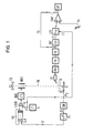
- a finely focused primary electron beam PE is generated in the electron-optical column of an electron beam measuring device known, for example, from US Pat. Nos. 4,220,853 or 4,223,220.
- This electron-optical column has, in addition to a large number of diaphragms and magnetic lens systems (not shown in FIGS. 1 and 2 for reasons of clarity) for beam shaping, beam deflection and beam focusing, an electron gun EG consisting essentially of a cathode, anode and Wehnelt electrode, and one over the beam blanking generator BBG controlled beam blanking system BBS.
- a detector DT made up of a suction network and a scintillator is provided, for example, to detect the secondary electrons SE triggered on the sample IC at the respectively selected point of impact of the primary electron beam PE.
- the detectable in the detector DT in its intensity at the individual measuring points due to the different potential, material and topography contrast fluctuating secondary electron current generates light pulses in the scintillator, which are fed to the photomultiplier PM via an optical fiber, and are converted here into a secondary electrical signal.
- the secondary electron signal generated in this way is then further amplified in a preamplifier PA, fed to a circuit SV for improving the signal-to-noise ratio (for example smoothing of the signal by low-pass filtering), and integrated in a downstream integrator INT over a specific time interval.
- the detector DT can also be preceded by a spectrometer SP, preferably an opposing field spectrometer, as is known, for example, from US Pat. No. 4,292,519, for measuring the shift in the energy distribution of the secondary electrons SE which is dependent on the sample potential.
- this spectrometer SP is indicated schematically by a flat counter-field electrode.
- An integrated circuit operating at nominal frequency is preferably provided as the sample IC, into which test programs adapted to the problem to be investigated are periodically fed via the control CON.
- characteristic signals defining the operating state then appear at nodes and conductor tracks during the test cycle, which signals can be compared to check the functionality with the signal profiles obtained, for example, from simulation calculations.
- the integrated circuit IC can of course be replaced by any sample which has conductive tracks or contact points at the points accessible for a primary electron beam PE.
- the method according to the invention allows the localization and mapping of the conductor tracks of an integrated circuit IC, which carry a specific, searched signal. Since the exemplary embodiment described below relates specifically to binary signals, the signal sought is then a specific bit pattern.
- the signal measured at the respectively selected measuring point of the sample IC is compared with the bit pattern sought using a correlation method.
- This correlation described below must be carried out for high-frequency signals (clock frequency> 5 MHz) because of the narrow bandwidth of the detector arrangement from the primary electron beam PE via the mechanism of the potential contrast.
- the amplitude or intensity of the primary electron current i PE is now modulated with the signal sought, for example by changing the primary electron beam PE according to the occurrence of time "HIGH and" LOW "values of the bit pattern g (t) sought and keyed in, and at the same time integrating the secondary electron current i SE measured in the detector DT, the correlation defined in equation 1) is being carried out.
- the non-linearity of the potential contrast characteristic interferes not in this context, since only binary signals g (t) and f (t) are present.
- the primary electron beam PE is, according to the invention, alternately modulated with the bit pattern g (t) sought and its negation, ie as a function of the "HIGH” and - occurring in the respective bit sequence "LOW" values are keyed in and out using the BBS beam blanking system.
- the bit pattern sought is read into the shift register SR before the start of the measurement, the content of which is shifted cyclically during the measurement with a frequency f 2 predetermined by the external clock signal CLK.
- the clock signal CLK can be obtained, for example, from the clock frequency nf2 generated by the control CON by frequency division.
- the output signal of the shift register SR corresponding to the bit pattern being sought is either negated or not negated via the EXOR gate to the beam blanking generator BBG controlling the beam blanking system BBS.
- the beam blanking system BBS can also be controlled directly via the amplified output signal of the EXOR gate.
- the integrator INT supplies an output signal whose amplitude changes with the switching frequency f 1 between the extreme values c min and c max defined by equations 3) and 4).
- the fluctuation amplitude ⁇ c: c max - c min 5) is therefore always at a maximum if the conductor track in question leads the bit pattern sought.
- the fluctuation of the output signal generated by the integrator INT is always smaller than the variable c defined in equation 5).
- This also applies in particular to the areas of the sample IC in which, due to special materials (oxide layers) or the topography (edges), particularly many or a few secondary electrons SE are emitted and detected in the detector DT. Since the secondary electron signal determined in these areas essentially by the material or topography contrast and integrated in the integrator INT remains largely constant, regardless of the negated or non-negated bit pattern modulating the primary electron beam PE, the fluctuation of the integrator output signal is also less than in this case c.
- the integrator INT is followed by a lock-in amplifier LIV, the reference input RE of which is connected to the output of the signal generator G.
- a phase-sensitive detector LIV for example, a bandpass filter tuned to the switching frequency f 1 with a downstream amplitude demodulator (for example, a peak value rectifier can be used).
- the fluctuation amplitude is compared with the variable response threshold TH in the comparator CMP, the positive input of which is connected to the output signal of the lock-in amplifier LIV.
- the comparator CMP always only generates then a signal when the fluctuation of the integrator output signal lies above the response threshold TH, that is to say whenever the respective measuring point leads the bit pattern sought in phase.
- an integrator as an independent component can be dispensed with entirely, since for high frequencies the detector DT and for low frequencies with a suitable choice of the scanning speed the CRT of the scanning electron microscope itself have an integrating effect.
- the conductor tracks of the sample IC that carry a specific bit pattern their surface is scanned line by line or point by point with the primary electron beam PE. This scanning must take place so slowly that the correlation method described above is actually carried out at every point on the surface within the time interval in which the expected signal can occur.
- the primary corpuscular beam must therefore remain positioned at every measuring point at least during the integration period. If this is not the case, the measurement can be carried out periodically.
- the output signal of the comparator CMP is recorded as a function of the measuring point which is respectively acted upon by the primary electron beam PE.
- a simple recording possibility is to use the output signal of the comparator CMP to modulate the intensity of the write beam of the picture tube CRT, which is deflected synchronously with the primary electron beam PE, so that all conductor tracks which carry the signal sought are displayed brightly.
- Output signal of the comparator CMP superimpose a topography signal (for example the conventional secondary electron image of the sample IC) and display it at the same time. In Fig. 1, this is indicated schematically by the signal line TS.
- the phase at which the check is carried out can be set via the delay element DL. Since only the phase difference is of interest, the delay element DL can of course also be arranged between the control CON and probe IC.
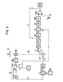
- An arrangement according to the invention with which this check can be carried out in a phase-independent manner and with which it can thus be tested whether the expected bit pattern is present at the measuring point at all is shown in FIG. 2, in the same reference numerals the same arrangement elements already described in connection with FIG. 1 describe.
- the electrically controllable delay element DL is driven by a generator GDL with the frequency f3, so that with the delay time the phase position of the primary electron beam PE modulated with the bit pattern sought or with its negation periodically with the frequency relative to the signal present at the measuring point f3 changes.
- the output signal of the integrator INT in addition to the signal component generated by switching the EXOR gate with the frequency f 1 also a signal component with the generally lower frequency f 3 if the measuring point leads the bit pattern sought.
- the signal component with the frequency f 1 can be filtered out again with the aid of a phase-sensitive detector, so that a LIV at the output of the lock-in amplifier shown in FIG Signal of frequency f3 can be tapped, which is fed to the input of the bandpass filter BP tuned to this frequency.
- the amplitude of this signal of frequency f3 is then determined in the downstream amplitude demodulator AMD, and compared in the comparator CMP with the variable response threshold TH, the comparator output signal depending on the location of the measuring point on the sample IC being recorded again or for controlling the intensity of the CRT can be used.
- the amplitude demodulator AMD is of course also superfluous.
- the frequency f 1 with which the EXOR gate is switched also less than the frequency f 3 with which the delay element DL is driven. In this case, however, you must first filter out the frequency f3 and then only the frequency f1 from the secondary electron signal, since the frequency f1 now appears as a modulation on the frequency f3 now acting as the carrier frequency.
- the lock-in amplifier LIV and the bandpass filter BP with a downstream amplitude demodulator AMD then appear in reverse order within the signal chain.
- a change in the phase position of the primary electron beam PE modulated with the bit pattern or its negation relative to the signal present at the measuring point can also be achieved simply by changing the frequency f 2 with which the bit sequence in the shift register SR is shifted cyclically, and by the Control CON generated clock frequency slightly offset from each other.
- the signal that can then be tapped at the output of the lock-in amplifier LIV with the predetermined differential frequency can again be fed to a bandpass filter tuned to this frequency.
- the upper limit frequency is determined by the beam blanking system BBS used. Since beam blanking systems BBS which are already operating in the GHz range are currently available, the arrangements according to the invention can be used to check integrated circuits IC under real operating conditions.
- the secondary electron current i SE that is alternately modulated with the bit pattern sought or its negation.
- a secondary electron spectrometer SP as is known, for example, from US Pat. No. 4,292,419, can be used as the modulator, in which the signal or bit pattern or its negation sought is the height of the potential wall built up in the spectrometer SP and thus also the intensity controls the secondary electron current i SE detectable in the detector DT.
- the output signal of the EXOR gate in a modification of the arrangements shown in FIGS.
- the advantage of this method is, in particular, that no BBS beam blanking system is required.
- the limit frequency that can be achieved with such an arrangement is, however, due to the relatively high capacity of the spectrometer SP, lower than that of the arrangements according to FIGS. 1 and 2.
- a detector DT can also be used to modulate the secondary electron current i SE . or bit pattern is controlled.
- the output signal of the EXOR gate is advantageously fed to an input of an adder, the output of which is in turn connected to the suction electrode of the detector DT. Otherwise the electrode for signal processing shown in FIGS. 1 and 2 remains unchanged.
- the secondary electron signal generated in signal processing (for example a detector-photomultiplier-amplifier arrangement) is modulated with the desired signal or bit pattern, for example with the aid of a gate circuit.
- the beam blanking system BBS and the associated signal generator BBG an arrangement for carrying out this method has all the circuit elements shown in FIGS. 1 and 2 and additionally a mixer arranged, for example, between the circuit SV for improving the signal-to-noise ratio and the integrator INT on. A second input of this mixer is in turn connected to the output of the EXOR gate.
- a multiplier can be used for the sought analog signal, for example a simple electronic switch for sought digital signals (bit patterns).
- This identification can be used to filter out the associated fluctuation amplitude from the processed secondary electron signal with the aid of a suitable filter or demodulator.
- a simple way of implementing this is, for example, to control the input B of the EXOR gate via a random bit sequence generator (a so-called pn or p seudo n oise generator) in the arrangement shown in FIG. 1 and the fluctuation amplitude of interest with the aid of a Filter out the random bit sequence of coordinated correlators.
- the secondary electron signal measured at every point of the sample IC does not have to arise exclusively through potential contrast.
- Any other contrast mechanism in which the secondary electrons SE are influenced by a signal present at the measuring point is suitable for this.
- the secondary electrons SE are deflected by local magnetic fields when using magnetic bubble memories as a sample IC (magnetic contrast).
- the invention is of course not limited to the use of electrons as primary and secondary corpuscles.
- ions or other corpuscles can also be considered as primary or secondary corpuscles.
- Lasers can of course also be used to generate a primary beam.
Abstract
Zur Überprüfung der Funktionsweise mikroelektronischer Bauelemente müssen insbesondere während der Entwicklungsphase Messungen im Innern hochintegrierter Schaltungen durchgeführt werden. Von besonderem Interesse für den Entwickler solcher Bauelemente ist hierbei die Lokalisierung und Abbildung der Bereiche einer zu untersuchenden Probe (IC), die bestimmte, den Betriebszustand der Schaltung charakterisierende Signale führen. Zur Lokalisierung der bestimmte elektrische Signale führender Punkte wird vorgeschlagen, das am jeweiligen Messpunkt anliegende Signal mit einem Primärstrahl (PE) abzutasten, und ein in einer Detektoranordnung (DT) abgeleitetes sekundäres Signal durch ein Korrelationsverfahren mit dem erwarteten oder gesuchten Signal zu vergleichen. Zur Durchführung der Korrelation wird hierbei insbesondere die Intensität des Primärstrahles (PE) oder der Strom der Sekundärkorpuskel (SE) abwechselnd mit dem gesuchten oder erwarteten Signal bzw. dem hieraus jeweils durch Negation erzeugten Signal moduliert und das gemessene Sekundärkorpuskelsignal aufintegriert. Der sich mit der durch den Signalwechsel vorgegebenen Frequenz (f1) ändernde Anteil des integrierten Sekundärkorpuskelsignals wird ausgefiltert und einer Bewerteschaltung (CMP) zugeführt, deren Ausgangssignal beispielsweise die Helligkeit des Bildschirms eines Sichtgerätes (CRT) steuert.To check the functioning of microelectronic components, measurements must be carried out inside highly integrated circuits, particularly during the development phase. Of particular interest for the developer of such components is the localization and mapping of the areas of a sample to be examined (IC) which carry certain signals that characterize the operating state of the circuit. To localize the specific electrical signals of leading points, it is proposed to scan the signal present at the respective measuring point with a primary beam (PE) and to compare a secondary signal derived in a detector arrangement (DT) by means of a correlation method with the expected or sought signal. To carry out the correlation, in particular the intensity of the primary beam (PE) or the current of the secondary corpuscles (SE) are alternately modulated with the sought or expected signal or the signal generated therefrom by negation, and the measured secondary corpuscle signal is integrated. The portion of the integrated secondary body signal that changes with the frequency (f1) predetermined by the signal change is filtered out and fed to an evaluation circuit (CMP), the output signal of which controls, for example, the brightness of the screen of a display device (CRT).
Description
Die Erfindung betrifft ein Verfahren zur Lokalisierung und Abbildung der ein bestimmtes zeitabhängiges Signal führenden Punkte einer Probe nach dem Oberbegriff des Patentanspruchs 1, und eine Anordnung zur Durchführung des Verfahrens nach dem Obergriff des Patentanspruchs 14.The invention relates to a method for localizing and mapping the points of a sample carrying a specific time-dependent signal, and an arrangement for carrying out the method according to the preamble of claim 14.
Die Überprüfung der Funktionsweise hochintegrierter Schaltungen erfolgt üblicherweise in rechnergesteuerten Testsystemen, in denen vorhandene Fehler durch Analyse der an den Ausgängen der untersuchten Schaltung in Abhängigkeit von den jeweils eingespeisten Bitmustern gemessenen Spannungspegel zwar erkannt, aber nur sehr schwer lokalisiert werden können. Deshalb müssen insbesondere während der Entwicklungsphase zusätzliche Messungen im Innern hochintegrierter Schaltungen durchgeführt werden. Als für diese Zwecke besonders geeignet haben sich die in allen Bereichen der Entwicklung und Fertigung mikroelektronischer Bauelemente eingesetzten Elektronenstrahl-Meßverfahren herausgestellt, mit denen beispielsweise die dynamische Potentialverteilung in integrierten Schaltungen abgebildet (hier sind insbesondere die dem Fachmann unter der Bezeichnung "Voltage Coding" bzw. "Logic-State Mapping" bekannten Verfahren zu nennen) oder der zeitliche Potentialverlauf an einzelnen Knotenpunkten bestimmt werden kann ("Waveform Measurement").The functioning of highly integrated circuits is usually checked in computer-controlled test systems, in which existing errors can be detected by analyzing the voltage levels measured at the outputs of the examined circuit depending on the bit patterns fed in, but are very difficult to localize. This is why additional measurements must be carried out inside highly integrated circuits, especially during the development phase. The electron beam measuring methods used in all areas of development and production of microelectronic components have been found to be particularly suitable for these purposes, with which, for example, the dynamic potential distribution is mapped in integrated circuits (here in particular those known to the person skilled in the art under the name "voltage coding" or "Logic-state mapping" known methods) or the temporal course of potential at individual nodes can be determined ("waveform measurement").
Ein Verfahren zur Lokalisierung und Abbildung der Leiterbahnen einer integrierten Schaltung die ein Signal einer bestimmten Frequenz führen, ist aus der Veröffentlichung von H.-D. Brust "Frequency Tracing and Mapping: Novel Electron Beam Testing Methods" (Proceedings der Microciruit Engineering Conference, Berlin, September 1984, Seite 412 bis 425) bekannt. Mit diesem bekannten Verfahren kann allerdings nicht zwischen Signalen gleicher Frequenz aber unterschiedlichen Signalverlaufs unterschieden werden.A method for locating and mapping the conductor tracks of an integrated circuit which carry a signal of a specific frequency is from the publication by H.-D. Chest "Frequency Tracing and Mapping: Novel Electron Beam Testing Methods" (Proceedings of the Microciruit Engineering Conference, Berlin, September 1984, pages 412 to 425). With this known method, however, it is not possible to differentiate between signals of the same frequency but different signal profiles.
In der deutschen Patentanmeldung P 34 28 965.8 wurde deshalb ein Verfahren vorgeschlagen, mit dem die, ein bestimmtes elektrisches Signal führenden Leiterbahnen eines ICs lokalisiert und abgebildet werden können. Bei diesem sogenannten "Logic-State Tracing"-Verfahren (LST) werden allerdings nicht nur die das gesuchte Signal führenden Leiterbahnen hell auf einem Sichtgerät dargestellt, sondern unter Umständen auch die Bereiche der untersuchten Probe, in denen aufgrund des Material- oder Topographiekontrastes besonders hohe oder niedrige Sekundärelektronenströme auftreten.In the German patent application P 34 28 965.8, a method was therefore proposed with which the conductor tracks of an IC carrying a specific electrical signal can be located and mapped. With this so-called "logic-state tracing" method (LST), however, not only the conductor tracks carrying the signal sought are shown brightly on a display device, but also, under certain circumstances, the areas of the examined sample in which particularly high due to the material or topography contrast or low secondary electron currents occur.
Der vorliegenden Erfindung liegt die Aufgabe zugrunde, ein Verfahren und eine Anordnung der eingangs genannten Art anzugeben, mit deren Hilfe des möglich ist zu überprüfen, ob an einem Punkt einer zu untersuchenden Probe das erwartete, durch einen in der Probe ablaufenden periodischen Vorgang hervorgerufene Signal vorliegt, bzw. bei fehlerhaften Proben festzustellen, ob ein bestimmtes Signal überhaupt noch auftritt. Weiterhin soll sichergestellt sein, daß der störende Einfluß des Material- und Topographiekontrastes weitgehend unterdrückt wird.The present invention is based on the object of specifying a method and an arrangement of the type mentioned at the beginning, with the aid of which it is possible to check whether the expected signal caused by a periodic process occurring in the sample is present at a point of a sample to be examined , or in the case of defective samples, to determine whether a certain signal is still occurring. Furthermore, it should be ensured that the disturbing influence of the material and topography contrast is largely suppressed.
Diese Aufgabe wird erfindungsgemäß durch ein Verfahren nach Anspruch 1 und durch eine Anordnung nach Anspruch 14 gelöst. Ausgestaltungen und Vorteile der Erfindung sind in den Unteransprüchen, der Beschreibung und der Zeichnung dargestellt.According to the invention, this object is achieved by a method according to claim 1 and solved by an arrangement according to claim 14. Embodiments and advantages of the invention are shown in the subclaims, the description and the drawing.
Der mit der Erfindung erzielbare Vorteil liegt insbesondere darin, daß durch Unterdrückung des störenden Einflusses des Material- und Topographiekontrastes nur die, das gesuchte Signal führenden Bereiche der Probe (beispielsweise Leiterbahnen einer integrierten Schaltung) abgebildet werden.The advantage that can be achieved with the invention is, in particular, that by suppressing the disruptive influence of the material and topography contrast, only the regions of the sample that carry the signal sought (for example conductor tracks of an integrated circuit) are imaged.
Die Erfindung wird nachfolgend anhand der Zeichnungen näher erläutert. Dabei zeigen:
- Fig. 1 eine Anordnung zur Durchführung des erfingsgemässen Verfahrens
- Fig. 2 eine Weiterbildung der Anordnung nach Fig. 1
- Fig. 1 shows an arrangement for performing the inventive method
- 2 shows a development of the arrangement according to FIG. 1
Bei der in Fig. 1 dargestellten Anordnung zur Durchführung des erfindungsgemäßen Verfahrens wird ein fein gebündelter Primärelektronenstrahl PE in der elektronenoptischen Säule eines beipielsweise aus den US Patentschriften 4 220 853 oder 4 223 220 bekannten Elektronenstrahl-Meßgerätes erzeugt. Diese elektronenoptische Säule weist neben einer Vielzahl, in den Fig. 1 und 2 aus Gründen der Übersichtlichkeit nicht dargestellten Blenden und magnetischen Linsensystemen zur Strahlformung, Strahlablenkung und zur Strahlfokussierung, eine im wesentlichen aus Kathode, Anode und Wehnelt-Elektrode bestehende Elektronenkanone EG und ein über den Strahlaustastgenerator BBG angesteuertes Strahlaustastsystem BBS auf. Zum Nachweis der am jeweils gewählten Auftreffpunkt des Primärelektronenstrahls PE auf der Probe IC ausgelösten Sekundärelektronen SE ist beispielsweise ein aus Absaugnetz und Szintillator aufgebauter Detektor DT vorgesehen. Der im Detektor DT nachweisbare, in seiner Intensität an den einzelnen Meßpunkten infolge des unterschiedlichen Potential-, Material- und Tophographiekontrastes schwankende Sekundärelektronenstrom erzeugt im Szintillator Lichtimpulse, die über einen Lichtleiter dem Photomultiplier PM zugeführt, und hier in ein sekundäres elektrisches Signal umgewandelt werden. Anschliessend wird das so erzeugte Sekundärelektronensignal in einem Vorverstärker PA weiter verstärkt, einer Schaltung SV zur Verbesserung des Signal-Rausch Verhältnises zugeführt (beispielsweise Glättung des Signals durch Tiefpassfilterung), und in einem nachgeschalteten Integrator INT über ein bestimmtes Zeitintervall aufintegriert. Dem Detektor DT kann noch ein Spektrometer SP, vorzugsweise ein Gegenfeldspektrometer wie es beispielsweise aus der US Patentschrift 4 292 519 bekannt ist, zur Messung der vom Probenpotential abhängigen Verschiebung der Energieverteilung der Sekundärelektronen SE vorgeschaltet sein. In Fig. 1 ist dieses Spektrometer SP schematisch durch eine ebene Gegenfeldelektrode angedeutet.In the arrangement shown in FIG. 1 for carrying out the method according to the invention, a finely focused primary electron beam PE is generated in the electron-optical column of an electron beam measuring device known, for example, from US Pat. Nos. 4,220,853 or 4,223,220. This electron-optical column has, in addition to a large number of diaphragms and magnetic lens systems (not shown in FIGS. 1 and 2 for reasons of clarity) for beam shaping, beam deflection and beam focusing, an electron gun EG consisting essentially of a cathode, anode and Wehnelt electrode, and one over the beam blanking generator BBG controlled beam blanking system BBS. A detector DT made up of a suction network and a scintillator is provided, for example, to detect the secondary electrons SE triggered on the sample IC at the respectively selected point of impact of the primary electron beam PE. The detectable in the detector DT, in its intensity at the individual measuring points due to the different potential, material and topography contrast fluctuating secondary electron current generates light pulses in the scintillator, which are fed to the photomultiplier PM via an optical fiber, and are converted here into a secondary electrical signal. The secondary electron signal generated in this way is then further amplified in a preamplifier PA, fed to a circuit SV for improving the signal-to-noise ratio (for example smoothing of the signal by low-pass filtering), and integrated in a downstream integrator INT over a specific time interval. The detector DT can also be preceded by a spectrometer SP, preferably an opposing field spectrometer, as is known, for example, from US Pat. No. 4,292,519, for measuring the shift in the energy distribution of the secondary electrons SE which is dependent on the sample potential. In Fig. 1, this spectrometer SP is indicated schematically by a flat counter-field electrode.
Als Probe IC ist vorzugsweise eine mit Nennfrequenz arbeitende integrierte Schaltung vorgesehen, in die man über die Ansteuerung CON der zu untersuchenden Problemstellung angepaßte Testprogramme periodisch einspeist. Entsprechend der Schaltungsstruktur der Probe IC treten dann während des Testzyklus an Knotenpunkten und Leiterbahnen charakteristische, den Betriebszustand definierende Signale auf, die zur Überprüfung der Funktionsweise mit den beispielsweise aus Simulationsrechnungen gewonnenen Signalverläufen verglichen werden können.An integrated circuit operating at nominal frequency is preferably provided as the sample IC, into which test programs adapted to the problem to be investigated are periodically fed via the control CON. Corresponding to the circuit structure of the probe IC, characteristic signals defining the operating state then appear at nodes and conductor tracks during the test cycle, which signals can be compared to check the functionality with the signal profiles obtained, for example, from simulation calculations.
Die integrierte Schaltung IC kann selbstverständlich durch jede Probe ersetzt werden, die an den für einen Primärelektronenstrahl PE zugänglichen Stellen elektrische Signale führende Leiterbahnen oder Kontaktpunkte aufweist.The integrated circuit IC can of course be replaced by any sample which has conductive tracks or contact points at the points accessible for a primary electron beam PE.
Das erfindungsgemäße Verfahren erlaubt die Lokalisierung und Abbildung der Leiterbahnen einer integrierten Schaltung IC, die ein bestimmtes, gesuchtes Signal führen. Da sich das im folgenden beschriebene Ausführungsbeispiel speziell auf binäre Signale bezieht ist das gesuchte Signal dann ein bestimmtes Bitmuster.The method according to the invention allows the localization and mapping of the conductor tracks of an integrated circuit IC, which carry a specific, searched signal. Since the exemplary embodiment described below relates specifically to binary signals, the signal sought is then a specific bit pattern.
Wie schon bei dem in der deutschen Patentanmeldung P 34 28 965.8 vorgeschlagenen Verfahren wird das an dem jeweils ausgewählten Meßpunkt der Probe IC gemessene Signal mit Hilfe eines Korrelationsverfahrens mit dem gesuchten Bitmuster verglichen. Diese nachfolgend beschriebene Korrelation muß bei hochfrequenten Signalen (Taktfrequenz > 5 MHz) wegen der geringen Bandbreite der Detektoranordnung vom Primärelektronenstrahl PE über den Mechanismus des Potentialkontrastes durchgeführt werden.As with the method proposed in German patent application P 34 28 965.8, the signal measured at the respectively selected measuring point of the sample IC is compared with the bit pattern sought using a correlation method. This correlation described below must be carried out for high-frequency signals (clock frequency> 5 MHz) because of the narrow bandwidth of the detector arrangement from the primary electron beam PE via the mechanism of the potential contrast.
Bezeichnet f(t) das Signal an einem Punkt der Probe IC, und g(t) das gesuchte Bitmuster, so muß die in Gleichung 1) definierte Korrelation ausgeführt werden.
c:= ∫ f(t)·g(t)·dt 1)
Da der Sekundärelektronenstrom iSE proportional zum Primärelektronenstrom iPE ist, und zudem vom Signal f(t) am Meßpunkt abhängt gilt
iSE = h(f(t))·iPE 2)
wobei h(f(t)) den Einfluß der Potentialkontrastkennlinie auf den Sekundärelektronenstrom iSE kennzeichnet.If f (t) denotes the signal at a point of the sample IC and g (t) the bit pattern sought, the correlation defined in equation 1) must be carried out.
c: = ∫ f (t) g (t) dt 1)
Since the secondary electron current i SE is proportional to the primary electron current i PE and also depends on the signal f (t) at the measuring point
i SE = h (f (t)) i PE 2)
where h (f (t)) characterizes the influence of the potential contrast characteristic on the secondary electron current i SE .
Moduliert man nun den Primärelektronenstrom iPE in seiner Amplitude oder Intensität mit den gesuchten Signal, indem man beispielsweise den Primärelektronenstrahl PE entsprechend dem zeitlichen Auftreten der "HIGH- und "LOW"-Werte des gesuchten Bitmusters g(t) ein- und austastet, und integriert gleichzeitig den im Detektor DT gemessenen Sekundärelektronenstrom iSE, so wird gerade die in Gleichung 1) definierte Korrelation ausgeführt. Die Nichtliniarität der Potentialkontrastkennlinie stört in diesem Zusammenhang nicht, da nur binäre Signale g(t) und f(t) vorliegen.If the amplitude or intensity of the primary electron current i PE is now modulated with the signal sought, for example by changing the primary electron beam PE according to the occurrence of time "HIGH and" LOW "values of the bit pattern g (t) sought and keyed in, and at the same time integrating the secondary electron current i SE measured in the detector DT, the correlation defined in equation 1) is being carried out. The non-linearity of the potential contrast characteristic interferes not in this context, since only binary signals g (t) and f (t) are present.
Stimmen das gesuchte Bitmuster g(t) und das Signal am Meßpunkt f(t) innerhalb des gewählten Integrationszeitraumes in der Reihenfolge ihrer "HIGH"- und "LOW"-Werte und in der Phase überein, so ist der Wert des Integrals maximal
cmax = ∫ f(t)·g(t)·dt falls g(t) ≡ f(t) 3)
Ist hingegen das gesuchte Bitmuster g(t) gerade die negation des Signals f(t), so ist der Wert des Integrals minimal
cmin = ∫ f(t)·g(t)·dt falls g(t) ≡ Neg(f(t)) 4)
If the bit pattern g (t) sought and the signal at the measuring point f (t) match within the selected integration period in the order of their "HIGH" and "LOW" values and in phase, the value of the integral is maximum
c max = ∫ f (t) g (t) dt if g (t) ≡ f (t) 3)
If, on the other hand, the bit pattern g (t) sought is just the negation of the signal f (t), the value of the integral is minimal
c min = ∫ f (t) g (t) dt if g (t) ≡ Neg (f (t)) 4)
Für alle anderen Signale f(t) bewegt sich der Wert des Integrals zwischen diesen Grenzen cmax und cmin. Dies ist auch dann der Fall, wenn der Meßpunkt das gesuchte Bitmuster führt, dieses Bitmuster aber zeitlich verzögert, also phasenverschoben auftritt.For all other signals f (t) the value of the integral moves between these limits c max and c min . This is also the case if the measuring point leads the bit pattern sought, but this bit pattern is delayed, ie occurs out of phase.
Zur Unterdrückung des die Messungen in unerwünschter Weise beeinflußenden Material- oder Topographiekontrastes wird der Primärelektronenstrahl PE erfindungsgemäß abwechselnd mit dem gesuchten Bitmuster g(t) und dessen Negation moduliert, d. h. in Abhängigkeit von den in der jeweiligen Bitfolge auftretenden "HIGH"- und "LOW"-Werten mit Hilfe des Strahlaustastsystems BBS ein- und ausgetastet.To suppress the material or topography contrast which undesirably influences the measurements, the primary electron beam PE is, according to the invention, alternately modulated with the bit pattern g (t) sought and its negation, ie as a function of the "HIGH" and - occurring in the respective bit sequence "LOW" values are keyed in and out using the BBS beam blanking system.
Hierzu wird das gesuchte Bitmuster vor Beginn der Messung in das Schieberegister SR eingelesen, dessen Inhalt man während der Messung mit einer durch das äußere Taktsignal CLK vorgegebenen Frequenz f₂ zyklisch verschiebt. Das Taktsignal CLK kann beispielsweise aus der von der Ansteuerung CON erzeugte Taktfrequenz nf₂ durch Frequenzteilung gewonnen werden. Zur Modulation des Primärelektronenstrahls PE wird das dem gesuchten Bitmuster entsprechende Ausgangssignal des Schieberegisters SR über das EXOR-Gatter wahlweise negiert oder nichtnegiert dem das Strahlaustastsystem BBS steuernden Strahlaustastgenerator BBG zugeführt.For this purpose, the bit pattern sought is read into the shift register SR before the start of the measurement, the content of which is shifted cyclically during the measurement with a frequency f 2 predetermined by the external clock signal CLK. The clock signal CLK can be obtained, for example, from the clock frequency nf₂ generated by the control CON by frequency division. To modulate the primary electron beam PE, the output signal of the shift register SR corresponding to the bit pattern being sought is either negated or not negated via the EXOR gate to the beam blanking generator BBG controlling the beam blanking system BBS.
Die Ansteuerung des Strahlaustastsystems BBS kann hierbei auch direkt über das verstärkte Ausgangssignal des EXOR-Gatters erfolgen.The beam blanking system BBS can also be controlled directly via the amplified output signal of the EXOR gate.
Zur Umschaltung des EXOR-Gatters von der nichtnegierenden auf die negierende Betriebsweise wird dessen Eingang B mit dem Ausgang des Signalgenerators G verbunden, wobei die durch den Signalgenerator G vorgegebene Umschaltfrequenz f₁ klein im Vergleich zur Wiederholfrequenz der gesuchten Bitmusterfolge am jeweiligen Meßpunkt gewählt werden muß.To switch the EXOR gate from the non-negating to the negating mode, its input B is connected to the output of the signal generator G, the switching frequency predetermined by the signal generator G f₁ small compared to the repetition frequency of the bit pattern sequence sought at the respective measuring point.
Ist der Primärelektronenstrahl PE beispielsweise auf eine das gesuchte Bitmuster führenden Leiterbahn positioniert, so liefert der Integrator INT ein Ausgangssignal, dessen Amplitude mit der Umschaltfrequenz f₁ zwischen den durch die in Gleichung 3) und 4) definierten Extremwerte cmin und cmax wechselt. Die Schwankungsamplitude
Δ c: = cmax - cmin 5)
ist also immer dann maximal, wenn die betreffende Leiterbahn das gesuchte Bitmuster führt.If the primary electron beam PE is positioned, for example, on a conductor track leading the desired bit pattern, the integrator INT supplies an output signal whose amplitude changes with the switching frequency f 1 between the extreme values c min and c max defined by equations 3) and 4). The fluctuation amplitude
Δ c: = c max - c min 5)
is therefore always at a maximum if the conductor track in question leads the bit pattern sought.
Liegt das gesuchte Bitmuster hingegen nicht vor, bzw. tritt es zeitlich verzögert, also phasenverschoben auf, so ist die Schwankung des vom Integrator INT erzeugten Ausgangssignals stets kleiner als die in Gleichunng 5) definierte Größe c. Dies gilt insbesondere auch für die Bereiche der Probe IC, in denen aufgrund spezieller Materialien (Oxidschichten) oder der Topographie (Kanten) besonders viele oder wenige Sekundäreelektronen SE emittiert und im Detektor DT nachgewiesen werden. Da das in diesen Bereichen im wesentlichen durch den Material- oder Topographiekontrast bestimmte und im Integrator INT aufintegrierte Sekundärelektronen-Signal weitgehend unabhängig von dem den Primärelektronenstrahl PE jeweils modulierenden negierten oder nichtnegierten Bitmuster nahezu konstant bleibt, ist die Schwankung des Integratorausgangsignals auch in diesem Falle kleiner als c. Um festzustellen, ob ein Punkt das gesuchte Signal führt, genügt es also, die Schwankung des Integratorausgangssignals beispielsweise mit einem phasenempfindlichen Detektor zu bestimmen, und diese mit einem Schwellenwert TH (Δc ≳ TH) zu vergleichen. Nach der in Fig. 1 dargestellten Anordnung ist dem Integrator INT ein Lock-in-Verstärker LIV nachgeschaltet, dessen Referenzeingang RE mit dem Ausgang des Signalgenerators G verbunden ist. Anstelle dieses phasenempfindlichen Detektors LIV kann beispielsweise ein, auf die Umschaltfrequenz f₁ abgestimmtes Bandpaßfilter mit nachgeschaltetem Amplitudendemodulator (hierfür kommt beispielsweise ein Spitzenwertgleichrichter in Betracht) eingesetzt werden. Der Vergleich der Schwankungsamplitude mit der variablen Ansprechschwelle TH erfolgt im Komparator CMP, dessen Plus-Eingang mit dem Ausgangssignal des Lock-in-Verstärkers LIV beschaltet ist. Der Komparator CMP erzeugt immer nur dann ein Signal, wenn die Schwankung des Integratorausgangssignals oberhalb der Ansprechschwelle TH liegt, also immer dann, wenn der jeweilige Meßpunkt das gesuchte Bitmuster phasenrichtig führt.If, on the other hand, the searched bit pattern is not available, or if it occurs with a time delay, ie out of phase, the fluctuation of the output signal generated by the integrator INT is always smaller than the variable c defined in equation 5). This also applies in particular to the areas of the sample IC in which, due to special materials (oxide layers) or the topography (edges), particularly many or a few secondary electrons SE are emitted and detected in the detector DT. Since the secondary electron signal determined in these areas essentially by the material or topography contrast and integrated in the integrator INT remains largely constant, regardless of the negated or non-negated bit pattern modulating the primary electron beam PE, the fluctuation of the integrator output signal is also less than in this case c. To determine whether a point is leading the signal sought, it is therefore sufficient to determine the fluctuation of the integrator output signal, for example using a phase-sensitive detector, and to compare it with a threshold value TH (Δc ≳ TH). According to the arrangement shown in FIG. 1, the integrator INT is followed by a lock-in amplifier LIV, the reference input RE of which is connected to the output of the signal generator G. Instead of this phase-sensitive detector LIV, for example, a bandpass filter tuned to the switching frequency f 1 with a downstream amplitude demodulator (for example, a peak value rectifier can be used). The fluctuation amplitude is compared with the variable response threshold TH in the comparator CMP, the positive input of which is connected to the output signal of the lock-in amplifier LIV. The comparator CMP always only generates then a signal when the fluctuation of the integrator output signal lies above the response threshold TH, that is to say whenever the respective measuring point leads the bit pattern sought in phase.
Unter Umständen kann auf einen Integrator als eigenständiges Bauelement ganz verzichtet werden, da für hohe Frequenzen der Detektor DT und für niedrige Frequenzen bei geeigneter Wahl der Rastergeschwindigkeit die Bildröhre CRT des Raster-Elektronenmikroskops selbst integrierend wirken.Under certain circumstances, an integrator as an independent component can be dispensed with entirely, since for high frequencies the detector DT and for low frequencies with a suitable choice of the scanning speed the CRT of the scanning electron microscope itself have an integrating effect.
Zur Darstellung der ein bestimmtes Bitmuster führenden Leiterbahnen der Probe IC wird deren Oberfläche zeilen- bzw. punktweise mit dem Primärelektronenstrahl PE abgetastet. Diese Abtastung muß hierbei so langsam erfolgen, daß das oben beschriebene Korrelationsverfahren an jedem Punkt der Oberfläche innerhalb des Zeitintervalles, in dem das erwartete Signal auftreten kann, auch tatsächlich durchgeführt wird. Der primäre Korpuskularstrahl muß also mindestens während der Integrationsdauer auf jedem Meßpunkt positioniert bleiben. Ist dies nicht der Fall, kann die Messung periodisch vorgenommen werden. Zur Abbildung der das gesuchte Bitmuster phasenrichtig führenden Oberflächenstrukturen der Probe IC zeichnet man das Ausgangssignal des Komparators CMP in Abhängigkeit vom jeweils mit dem Primärelektronenstrahl PE beaufschlagten Meßpunkt auf. Eine einfache Aufzeichnungsmöglichkeit besteht darin, das Ausgangssignal des Komparators CMP zur Modulation der Intensität des synchron mit dem Primärelektronenstrahl PE abgelenkten Schreibstrahls der Bildröhre CRT des Elektronenstrahl-Meßgerätes heranzuziehen, so daß alle Leiterbahnen, die das gesuchte Signal führen, hell dargestellt werden. Zur besseren Lokalisierung dieser Strukturen innerhalb der hochkomplexen Schaltungen kann es von Vorteil sein, dem Ausgangssignal des Komparators CMP ein Topographiesignal (beispielsweise das konventionelle Sekundärelektronenbild der Probe IC) zu überlagern und dieses gleichzeitig darzustellen. In Fig. 1 ist dies schematisch durch die Signalleitung TS angedeutet.To display the conductor tracks of the sample IC that carry a specific bit pattern, their surface is scanned line by line or point by point with the primary electron beam PE. This scanning must take place so slowly that the correlation method described above is actually carried out at every point on the surface within the time interval in which the expected signal can occur. The primary corpuscular beam must therefore remain positioned at every measuring point at least during the integration period. If this is not the case, the measurement can be carried out periodically. In order to image the surface structures of the sample IC that guide the sought-after bit pattern in phase, the output signal of the comparator CMP is recorded as a function of the measuring point which is respectively acted upon by the primary electron beam PE. A simple recording possibility is to use the output signal of the comparator CMP to modulate the intensity of the write beam of the picture tube CRT, which is deflected synchronously with the primary electron beam PE, so that all conductor tracks which carry the signal sought are displayed brightly. For better localization of these structures within the highly complex circuits, it can be advantageous to Output signal of the comparator CMP superimpose a topography signal (for example the conventional secondary electron image of the sample IC) and display it at the same time. In Fig. 1, this is indicated schematically by the signal line TS.
Mit der bisher beschriebenen Anordnung kann nur überprüft werden, ob an dem untersuchten Meßpunkt ein bestimmtes Bitmuster phasenrichtig auftritt. Die Phase zu der man die Überprüfung vornimmt, kann hierbei über das Verzögerungsglied DL eingestellt werden. Da nur die Phasendifferenz von Interesse ist, kann das Verzögerungsglied DL selbstverständlich auch zwischen Ansteuerung CON und Probe IC angeordnet werden. Eine erfindungsgemäße Anordnung mit der diese Überprüfung phasenunabhängig durchführbar ist, mit der also getestet werden kann, ob das erwartete Bitmuster am Meßpunkt überhaupt vorliegt, ist in Fig. 2 dargestellt, in der gleiche Bezugszeichen die gleichen, schon in Zusammenhang mit Fig. 1 beschriebenen Anordnungselemente bezeichnen.With the arrangement described so far, it can only be checked whether a certain bit pattern occurs in phase at the measuring point under investigation. The phase at which the check is carried out can be set via the delay element DL. Since only the phase difference is of interest, the delay element DL can of course also be arranged between the control CON and probe IC. An arrangement according to the invention with which this check can be carried out in a phase-independent manner and with which it can thus be tested whether the expected bit pattern is present at the measuring point at all is shown in FIG. 2, in the same reference numerals the same arrangement elements already described in connection with FIG. 1 describe.
Das elektrisch steuerbare Verzögerungsglied DL wird hierbei von einem Generator GDL mit der Frequenz f₃ angesteuert, so daß sich mit der Verzögerungszeit auch die Phasenlage des mit dem gesuchten Bitmuster bzw. mit dessen Negation modulierten Primärelektronenstrahls PE relativ zu dem am Meßpunkt anliegenden Signal periodisch mit der Frequenz f₃ ändert. Damit weist das Ausgangssignal des Integrators INT neben der durch das Umschalten des EXOR-Gatters erzeugten Signalkomponente mit der Frequenz f₁ auch eine Signalkomponente mit der im allgemeinen niedrigeren Frequenz f₃ auf, falls der Meßpunkt das gesuchte Bitmuster führt. Die Signalkomponente mit der Frequenz f₁ kann man wieder mit Hilfe eines phasenempfindlichen Detektors ausfiltern, so daß am Ausgang des in Fig. 2 dargestellten Lock-in-Verstärkers LIV ein Signal der Frequenz f₃ abgreifbar ist, das man dem Eingang des auf diese Frequenz abgestimmten Bandpaßes BP zuführt. Die Amplitude dieses Signals der Frequenz f₃ wird anschließend in dem nachgeschalteten Amplitudendemodulators AMD bestimmt, und in dem Komparator CMP mit der variablen Ansprechschwelle TH verglichen, wobei das Komparatorausgangssignal in Abhängigkeit von dem Ort des Meßpunktes auf der Probe IC wieder aufgezeichnet oder zur Steuerung der Intensität des Schreibstrahls der Bildröhre CRT herangezogen werden kann.The electrically controllable delay element DL is driven by a generator GDL with the frequency f₃, so that with the delay time the phase position of the primary electron beam PE modulated with the bit pattern sought or with its negation periodically with the frequency relative to the signal present at the measuring point f₃ changes. Thus, the output signal of the integrator INT in addition to the signal component generated by switching the EXOR gate with the frequency f ₁ also a signal component with the generally lower frequency f ₃ if the measuring point leads the bit pattern sought. The signal component with the frequency f 1 can be filtered out again with the aid of a phase-sensitive detector, so that a LIV at the output of the lock-in amplifier shown in FIG Signal of frequency f₃ can be tapped, which is fed to the input of the bandpass filter BP tuned to this frequency. The amplitude of this signal of frequency f₃ is then determined in the downstream amplitude demodulator AMD, and compared in the comparator CMP with the variable response threshold TH, the comparator output signal depending on the location of the measuring point on the sample IC being recorded again or for controlling the intensity of the CRT can be used.
Selbstverständlich kann man die Frequenz f₃ nicht nur mit einem Bandpaßfilter BP sondern auch phasenempfindlich, etwa mit Hilfe eines Lock-in-Verstärkers, ausfiltern. In diesem Fall wird natürlich auch der Amplitudendemodulator AMD überflüssig.Of course you can filter the frequency f₃ not only with a bandpass filter BP but also phase sensitive, for example with the help of a lock-in amplifier. In this case, the amplitude demodulator AMD is of course also superfluous.
Außerdem ist es möglich, die Frequenz f₁, mit der das EXOR-Gatter umgeschaltet wird, auch kleiner als die Frequenz f₃, mit der das Verzögerungsglied DL angesteuert wird, zu wählen. In diesem Fall muß man allerdings zuerst die Frequenz f₃ und dann erst die Frequenz f₁ aus dem Sekundärelektronensignal ausfiltern, da nun die Frequenz f₁ als Modulation auf der jetzt als Trägerfrequenz wirkenden Frequenz f₃ erscheint. In Fig. 2 treten dann der Lock-in-Verstärker LIV und das Bandpaßfilter BP mit nachgeschaltetem Amplitudendemodulator AMD innerhalb der Signalkette in umgekehrter Reihenfolge auf.In addition, it is possible to choose the frequency f 1 with which the EXOR gate is switched, also less than the frequency f 3 with which the delay element DL is driven. In this case, however, you must first filter out the frequency f₃ and then only the frequency f₁ from the secondary electron signal, since the frequency f₁ now appears as a modulation on the frequency f₃ now acting as the carrier frequency. In FIG. 2, the lock-in amplifier LIV and the bandpass filter BP with a downstream amplitude demodulator AMD then appear in reverse order within the signal chain.
Eine Änderung der Phasenlage des mit dem gesuchten Bitmuster bzw. dessen Negation modulierten Primärelektronenstrahles PE relativ zu dem am Meßpunkt anliegenden Signal ist auch einfach dadurch erreichbar, daß man die Frequenz f₂, mit dem die Bitfolge im Schieberegister SR zyklisch verschoben wird, und die von der Ansteuerung CON erzeugte Taktfrequenz leicht gegeneinander versetzt. Das dann am Ausgang des Lock-in-Verstärkers LIV abgreifbare Signal mit der vorgegebenen Differenzfrequenz kann wieder einem auf diese Frequenz abgestimmten Bandpaßfilter zugeführt werden.A change in the phase position of the primary electron beam PE modulated with the bit pattern or its negation relative to the signal present at the measuring point can also be achieved simply by changing the frequency f 2 with which the bit sequence in the shift register SR is shifted cyclically, and by the Control CON generated clock frequency slightly offset from each other. The signal that can then be tapped at the output of the lock-in amplifier LIV with the predetermined differential frequency can again be fed to a bandpass filter tuned to this frequency.
Bei den in den Fig. 1 und 2 dargestellten Anordnungen wird die obere Grenzfrequenz durch das verwendete Strahlaustastsystem BBS bestimmt. Da zur Zeit bereits in GHz-Bereich arbeitende Strahlaustastsysteme BBS zur Verfügung stehen, können die erfindungsgemäßen Anordnungen zur Überprüfung integrierter Schaltungen IC unter realen Betriebsbedingungen eingesetzt werden.In the arrangements shown in FIGS. 1 and 2, the upper limit frequency is determined by the beam blanking system BBS used. Since beam blanking systems BBS which are already operating in the GHz range are currently available, the arrangements according to the invention can be used to check integrated circuits IC under real operating conditions.
Nach einer weiteren Ausgestaltung der Erfindung wird im Unterschied zu den zuvor beschriebenen Anordnungen nicht der Primärelektronenstrahl PE, sondern der Sekundärelektronenstrom iSE abwechselnd mit dem gesuchten Bitmuster bzw. dessen Negation moduliert. Als Modulator kann ein Sekundärelektronen-Spektrometer SP, wie es beispielsweise aus der US Patentschrift 4 292 419 bekannt ist, eingesetzt werden, bei dem das gesuchte Signal- oder Bitmuster bzw. dessen Negation die Höhe des im Spektrometer SP aufgebauten Potentialwalls und damit auch die Intensität des im Detektor DT nachweisbaren Sekundärelektronenstromes iSE steuert. In einer Anordnung zur Durchführung dieses Verfahrens wird das Ausgangssignal des EXOR-Gatters in Abwandlung zu den in Fig. 1 und 2 dargestellten Anordnungen einem Eingang eines Addierers zugeführt, dessen Ausgang mit der Gegenfeldelektrode des Spektrometers SP verbunden ist. Die Ansteuerung der Gegenfeldelektrode über einen Addierer bietet insbesondere den Vorteil, daß der Arbeitspunkt des Spektrometers optimal eingestellt werden kann. Ansonsten bleibt die in den Fig. 1 und 2 dargestellte Meßkette zur Signalverarbeitung unverändert.According to a further embodiment of the invention, in contrast to the arrangements described above, it is not the primary electron beam PE, but the secondary electron current i SE that is alternately modulated with the bit pattern sought or its negation. A secondary electron spectrometer SP, as is known, for example, from US Pat. No. 4,292,419, can be used as the modulator, in which the signal or bit pattern or its negation sought is the height of the potential wall built up in the spectrometer SP and thus also the intensity controls the secondary electron current i SE detectable in the detector DT. In an arrangement for carrying out this method, the output signal of the EXOR gate, in a modification of the arrangements shown in FIGS. 1 and 2, is fed to an input of an adder, the output of which is connected to the counterfield electrode of the spectrometer SP. Controlling the counterfield electrode via an adder offers the particular advantage that the operating point of the spectrometer can be optimally adjusted. Otherwise, the measuring chain for signal processing shown in FIGS. 1 and 2 remains unchanged.
Der Vorteil dieses Verfahrens liegt insbesondere darin, daß kein Strahlaustastsystem BBS erforderlich ist. Die mit einer solchen Anordnung erreichbare Grenzfrequenz ist allerdings wegen der relativ hohen Kapazität des Spektrometers SP geringer als die der Anordnungen nach Fig. 1 und 2. Zur Modulation des Sekundärelektronenstromes iSE kann auch ein Detektor DT eingesetzt werden, dessen Absaugspannung vom dem gesuchten Signal- oder Bitmuster gesteuert wird. Auch in einer Anordnung zur Durchführung dieses Verfahrens wird das Ausgangssignal des EXOR-Gatters vorteilhafterweise einem Eingang eines Addierers zugeführt, dessen Ausgang wiederum mit der Absaugelektrode des Detektors DT verbunden ist. Ansonsten bleibt auch hier die in den Fig. 1 und 2 dargestellte Meßkette zur Signalverarbeitung unverändert.The advantage of this method is, in particular, that no BBS beam blanking system is required. The limit frequency that can be achieved with such an arrangement is, however, due to the relatively high capacity of the spectrometer SP, lower than that of the arrangements according to FIGS. 1 and 2. A detector DT can also be used to modulate the secondary electron current i SE . or bit pattern is controlled. Also in an arrangement for performing this method, the output signal of the EXOR gate is advantageously fed to an input of an adder, the output of which is in turn connected to the suction electrode of the detector DT. Otherwise the electrode for signal processing shown in FIGS. 1 and 2 remains unchanged.
Nach einer weiteren Ausgestaltung der Erfindung wird anstelle des Primärelektronenstrahles PE das in einer Signalverarbeitung (beispielsweise einer Detektor-Photomultiplier-Verstärkeranordnung) erzeugte Sekundärelektronensignal mit dem gesuchten Signal- oder Bitmuster, beispielsweise mit Hilfe einer Gate-Schaltung, moduliert. Eine Anordnung zur Durchführung dieses Verfahrens weist mit Ausnahme des Strahlaustastsystems BBS und des zugeordneten Signalgenerators BBG alle in den Fig. 1 und 2 dargestellten Schaltungselemente und zusätzlich noch einen beispielsweise zwischen der Schaltung SV zur Verbesserung des Signal-Rausch-Verhältnisses und dem Integrator INT angeordneten Mischer auf. Ein zweiter Eingang dieses Mischers ist hierbei wiederum mit dem Ausgang des EXOR-Gatters verbunden. Als Mischer kommt für das gesuchte analoge Signal beispielsweise ein Multiplizierer, für gesuchte digitale Signale (Bitmuster) beispielsweise ein einfacher elektronischer Schalter in Betracht.According to a further embodiment of the invention, instead of the primary electron beam PE, the secondary electron signal generated in signal processing (for example a detector-photomultiplier-amplifier arrangement) is modulated with the desired signal or bit pattern, for example with the aid of a gate circuit. With the exception of the beam blanking system BBS and the associated signal generator BBG, an arrangement for carrying out this method has all the circuit elements shown in FIGS. 1 and 2 and additionally a mixer arranged, for example, between the circuit SV for improving the signal-to-noise ratio and the integrator INT on. A second input of this mixer is in turn connected to the output of the EXOR gate. As a mixer, a multiplier can be used for the sought analog signal, for example a simple electronic switch for sought digital signals (bit patterns).
Nach einer weiteren Ausgestaltung der Erfindung ver zichtet man auf eine Modulation mit einer Frequenz f₁ und kennzeichnet stattdessen den Primär- bzw. Sekundärelektronenstrom bzw. das Sekundärelektronensignal auf andere Art und Weise durch eine Modulation.According to a further embodiment of the invention ver one waives for a modulation with a frequency f 1 and instead identifies the primary or secondary electron current or the secondary electron signal in a different way by modulation.
Diese Kennzeichnung kann dazu benutzt werden, die zugehörige Schwankungsamplitude mit Hilfe eines geeigneten Filters bzw. Demodulators aus dem verarbeiteten Sekundärelektronensignal auszufiltern. Eine einfache Möglichkeit der Realisierung besteht beispielsweise darin, in der in Fig. 1 dargestellten Anordnung den Eingang B des EXOR-Gatters über einen Zufallsbitfolgegenerator (ein sog. pn oder pseudo noise - Generator) anzusteuern und die interessierende Schwankungsamplitude mit Hilfe eines auf die Zufallsbitfolge abgestimmten Korrelators auszufiltern.This identification can be used to filter out the associated fluctuation amplitude from the processed secondary electron signal with the aid of a suitable filter or demodulator. A simple way of implementing this is, for example, to control the input B of the EXOR gate via a random bit sequence generator (a so-called pn or p seudo n oise generator) in the arrangement shown in FIG. 1 and the fluctuation amplitude of interest with the aid of a Filter out the random bit sequence of coordinated correlators.
Auch bei den oben beschriebenen Verfahren und Meßanordnungen kann es von Vorteil sein, dem Ausgangssignal zur zweidimensionalen Abbildung der untersuchten Probe IC das Sekundärelektronen-Topographiesignal oder ein anderes Topographiesignal zu überlagern. Dies erleichtert die Lokalisierung der abgebildeten, das gesuchte Signal- oder Bitmuster führenden Bereiche auf der Probenoberfläche.In the methods and measuring arrangements described above, it can also be advantageous to superimpose the secondary electron topography signal or another topography signal on the output signal for two-dimensional imaging of the sample IC under investigation. This facilitates the localization of the imaged areas on the sample surface that carry the desired signal or bit pattern.
Selbstverständlich muß das an jedem Punkt der Probe IC gemessene Sekundärelektronen-Signal nicht ausschließlich durch Potentialkontrast entstehen. Jeder andere Kontrastmechanismus, bei dem die Sekundärelektronen SE durch ein am Meßpunkt anliegendes Signal beeinflußt werden, ist hierfür geeignet. So werden die Sekundärelektronen SE beispielsweise bei Verwendung von Magnetblasenspeichern als Probe IC durch lokale magnetische Felder abgelenkt (Magnetischer Kontrast).Of course, the secondary electron signal measured at every point of the sample IC does not have to arise exclusively through potential contrast. Any other contrast mechanism in which the secondary electrons SE are influenced by a signal present at the measuring point is suitable for this. For example, the secondary electrons SE are deflected by local magnetic fields when using magnetic bubble memories as a sample IC (magnetic contrast).
Die Erfindung ist selbstverständlich nicht auf die Verwendung von Elektronen als Primär- und Sekundärkorpuskel beschränkt. So können neben Elektronen, je nach Anwendungsfall, auch Ionen oder andere Korpuskel als Primär- bzw. Sekundärkorpuskel in Betracht kommen. Zur Erzeugung eines Primärstrahls kann selbstverständlich auch Laser verwendet werden.The invention is of course not limited to the use of electrons as primary and secondary corpuscles. In addition to electrons, depending on the application, ions or other corpuscles can also be considered as primary or secondary corpuscles. Lasers can of course also be used to generate a primary beam.
Claims (25)
in einem Rastermikroskop, mit einem Primärstrahlerzeuger, mit Vorrichtungen zur Ablenkung und Fokussierung des Primärstrahles (PE) mit einer Ansteuerung zur Einspeisung von Versorgungsspannungen und/oder Signalen in die Probe, mit einer Detektoranordnung zum Nachweis sekundärer Korpuskel der eine Anordnung zur Signalverarbeitung nachgeordnet ist, mit einer Vorrichtung zur Modulation eines innerhalb der Anordnung zwischen dem Primärstrahlerzeuger und der Signalverarbeitung auftretenden Signals, und mit einer Schaltungsanordnung zur Ansteuerung der Vorrichtung zur Modulation, gekennzeichnet durch eine zwischen der Schaltungsanordnung (SR) und der Vorrichtung zur Modulation (BBS, SP) angeordnete Vorrichtung (EXOR) zur Negierung des bestimmten oder negierten Signals, und einem mit dieser Vorrichtung verbundenen ersten Signalgenerator (G) zu deren Umschaltung von einer negierenden in eine nichtnegierende Betriebsweise.14. Arrangement for localization and / or mapping of the points of a sample carrying a specific time-dependent signal
in a scanning microscope, with a primary beam generator, with devices for deflecting and focusing the primary beam (PE) with a control for feeding supply voltages and / or signals into the sample, with a detector arrangement for detecting secondary corpuscles, which is followed by an arrangement for signal processing one A device for modulating a within the array between the primary-ray generator and the signal processing signal appearing, and with a circuit arrangement for controlling the device for modulation, characterized by means disposed between the circuit arrangement (SR) and the device for modulation (BBS, SP) apparatus (EXOR ) for negating the determined or negated signal, and a first signal generator (G) connected to this device for switching it from a negating to a non-negating mode of operation.
Applications Claiming Priority (2)
| Application Number | Priority Date | Filing Date | Title |
|---|---|---|---|
| DE3544600 | 1985-12-17 | ||
| DE3544600 | 1985-12-17 |
Publications (2)
| Publication Number | Publication Date |
|---|---|
| EP0226913A2 true EP0226913A2 (en) | 1987-07-01 |
| EP0226913A3 EP0226913A3 (en) | 1988-10-05 |
Family
ID=6288654
Family Applications (1)
| Application Number | Title | Priority Date | Filing Date |
|---|---|---|---|
| EP86116960A Withdrawn EP0226913A3 (en) | 1985-12-17 | 1986-12-05 | Method and device for situating and/or displaying probe points carrying a characteristic time-dependent signal |
Country Status (4)
| Country | Link |
|---|---|
| US (1) | US4820977A (en) |
| EP (1) | EP0226913A3 (en) |
| JP (1) | JPS62156829A (en) |
| CA (1) | CA1254670A (en) |
Families Citing this family (10)
| Publication number | Priority date | Publication date | Assignee | Title |
|---|---|---|---|---|
| JPS6435838A (en) * | 1987-07-31 | 1989-02-06 | Jeol Ltd | Charged particle beam device |
| NL8802335A (en) * | 1988-09-21 | 1990-04-17 | Philips Nv | METHOD AND APPARATUS FOR PROCESSING A MATERIAL SURFACE ON SUB-MIKRON SCALE |
| DE3917411A1 (en) * | 1989-05-29 | 1990-12-06 | Brust Hans Detlef | METHOD AND ARRANGEMENT FOR FAST SPECTRAL ANALYSIS OF A SIGNAL AT ONE OR MULTIPLE MEASURING POINTS |
| EP0504944B1 (en) * | 1991-03-22 | 1998-09-23 | Nec Corporation | Method of analyzing fault using electron beam |
| JP2685425B2 (en) * | 1994-09-30 | 1997-12-03 | 株式会社東芝 | Liquid crystal element evaluation method |
| US5638005A (en) * | 1995-06-08 | 1997-06-10 | Schlumberger Technologies Inc. | Predictive waveform acquisition |
| US6466040B1 (en) * | 1997-08-01 | 2002-10-15 | Carl Zeiss Jena Gmbh | Three dimensional optical beam induced current (3-D-OBIC) |
| FR2841418A1 (en) * | 2002-06-20 | 2003-12-26 | Thomson Licensing Sa | DIGITAL DEVICE FOR CORRECTING THE IMAGE FORMED ON THE SCREEN OF A TUBE WITH CATHODE RAYS |
| US8754633B2 (en) | 2009-05-01 | 2014-06-17 | Dcg Systems, Inc. | Systems and method for laser voltage imaging state mapping |
| JP6014688B2 (en) * | 2013-01-31 | 2016-10-25 | 株式会社日立ハイテクノロジーズ | Compound charged particle beam system |
Citations (5)
| Publication number | Priority date | Publication date | Assignee | Title |
|---|---|---|---|---|
| GB2017941A (en) * | 1978-03-31 | 1979-10-10 | Siemens Ag | Monitoring variable voltage with an electron beam |
| EP0166814A1 (en) * | 1984-05-30 | 1986-01-08 | Siemens Aktiengesellschaft | Method and device for detecting and displaying a measuring point which carries a voltage of at least one certain frequency |
| EP0172470A1 (en) * | 1984-08-06 | 1986-02-26 | Siemens Aktiengesellschaft | Method and device for the detection and mapping of measuring points corresponding to a signal of a specific shape |
| EP0196958A2 (en) * | 1985-03-15 | 1986-10-08 | Schlumberger Technologies, Inc. | Electron beam test probe for integrated-circuit testing |
| EP0197362A1 (en) * | 1985-03-22 | 1986-10-15 | Siemens Aktiengesellschaft | Method making use of a scanning microscope to determine the points on a sample conducting a signal of a predetermined frequency |
Family Cites Families (11)
| Publication number | Priority date | Publication date | Assignee | Title |
|---|---|---|---|---|
| DE2813948A1 (en) * | 1978-03-31 | 1979-10-11 | Siemens Ag | METHOD FOR ELECTRONIC REPRESENTATION OF POTENTIAL DISTRIBUTION IN AN ELECTRONIC COMPONENT |
| JPS5571024A (en) * | 1978-11-24 | 1980-05-28 | Hitachi Ltd | Mark sensing method |
| DE2902495A1 (en) * | 1979-01-23 | 1980-07-31 | Siemens Ag | DEVICE FOR CONTACTLESS POTENTIAL MEASUREMENT |
| DE2903077C2 (en) * | 1979-01-26 | 1986-07-17 | Siemens AG, 1000 Berlin und 8000 München | Method for contactless potential measurement on an electronic component and arrangement for carrying out the method |
| DE3036660A1 (en) * | 1980-09-29 | 1982-05-19 | Siemens AG, 1000 Berlin und 8000 München | ARRANGEMENT FOR STROBOSCOPIC POTENTIAL MEASUREMENTS WITH AN ELECTRON BEAM MEASURING DEVICE |
| DE3036708A1 (en) * | 1980-09-29 | 1982-05-13 | Siemens AG, 1000 Berlin und 8000 München | ELECTRON BEAM MEASURING DEVICE FOR STROBOSCOPIC MEASUREMENT OF HIGH FREQUENCY PERIODIC PROCESSES |
| JPS5931549A (en) * | 1982-08-13 | 1984-02-20 | Hitachi Ltd | Image display system of stroboscopic scanning type electron microscope |
| JPS59141238A (en) * | 1983-02-01 | 1984-08-13 | Hitachi Ltd | Carrier life measuring device |
| JPS6070651A (en) * | 1983-09-28 | 1985-04-22 | Hitachi Ltd | Focusing method and device therefor |
| DE3407041A1 (en) * | 1984-02-27 | 1985-09-05 | Siemens AG, 1000 Berlin und 8000 München | METHOD FOR AUTOMATICALLY ADJUSTING THE WORKING POINT IN SIGNAL CURRENT MEASUREMENTS WITH CARPULAR RAY MEASURING DEVICES |
| DE3407071A1 (en) * | 1984-02-27 | 1985-08-29 | Siemens AG, 1000 Berlin und 8000 München | METHOD FOR AUTOMATICALLY SETTING THE VOLTAGE RESOLUTION IN CARPULAR RAY MEASURING DEVICES AND DEVICE FOR CARRYING OUT SUCH A METHOD |
-
1986
- 1986-12-05 EP EP86116960A patent/EP0226913A3/en not_active Withdrawn
- 1986-12-15 US US06/941,646 patent/US4820977A/en not_active Expired - Fee Related
- 1986-12-15 CA CA000525271A patent/CA1254670A/en not_active Expired
- 1986-12-16 JP JP61301099A patent/JPS62156829A/en active Pending
Patent Citations (5)
| Publication number | Priority date | Publication date | Assignee | Title |
|---|---|---|---|---|
| GB2017941A (en) * | 1978-03-31 | 1979-10-10 | Siemens Ag | Monitoring variable voltage with an electron beam |
| EP0166814A1 (en) * | 1984-05-30 | 1986-01-08 | Siemens Aktiengesellschaft | Method and device for detecting and displaying a measuring point which carries a voltage of at least one certain frequency |
| EP0172470A1 (en) * | 1984-08-06 | 1986-02-26 | Siemens Aktiengesellschaft | Method and device for the detection and mapping of measuring points corresponding to a signal of a specific shape |
| EP0196958A2 (en) * | 1985-03-15 | 1986-10-08 | Schlumberger Technologies, Inc. | Electron beam test probe for integrated-circuit testing |
| EP0197362A1 (en) * | 1985-03-22 | 1986-10-15 | Siemens Aktiengesellschaft | Method making use of a scanning microscope to determine the points on a sample conducting a signal of a predetermined frequency |
Non-Patent Citations (1)
| Title |
|---|
| PROCEEDINGS OF THE MICROCIRCUIT ENGINEERING CONFERENCE, Berlin, September 1984, Seiten 412-425, Academic Press, London, GB; H.D. BRUST et al.: "Frequency tracing and mapping: novel electron beam testing methods" * |
Also Published As
| Publication number | Publication date |
|---|---|
| CA1254670A (en) | 1989-05-23 |
| US4820977A (en) | 1989-04-11 |
| EP0226913A3 (en) | 1988-10-05 |
| JPS62156829A (en) | 1987-07-11 |
Similar Documents
| Publication | Publication Date | Title |
|---|---|---|
| EP0189777B1 (en) | Particle beam measuring method for the contactless testing of circuit networks | |
| DE2814049C2 (en) | ||
| DE2813948C2 (en) | ||
| EP0428663B1 (en) | Process and device for rapid spectral analysis of a signal at one or more measurement points | |
| DE2005682C3 (en) | Device for extracting the secondary electrons in a scanning electron microscope or an electron beam microanalyser | |
| DE2813947A1 (en) | METHOD FOR CONTACTLESS MEASUREMENT OF THE POTENTIAL DEVELOPMENT IN AN ELECTRONIC COMPONENT AND ARRANGEMENT FOR PERFORMING THE METHOD | |
| DE1943140B2 (en) | METHOD OF ANALYZING THE SURFACE POTENTIAL OF A DUTY | |
| EP0166814B1 (en) | Method and device for detecting and displaying a measuring point which carries a voltage of at least one certain frequency | |
| EP1801844A2 (en) | Method and apparatus for distance measurement | |
| EP0013876A1 (en) | Device for contactless potential measurement | |
| EP0226913A2 (en) | Method and device for situating and/or displaying probe points carrying a characteristic time-dependent signal | |
| EP0285896B1 (en) | Method for testing wire networks | |
| EP0172470B1 (en) | Method and device for the detection and mapping of measuring points corresponding to a signal of a specific shape | |
| EP0196531B1 (en) | Method for indirectly determining the intensity distribution of pulsed particle beams produced in a particle beam measuring instrument | |
| EP0310816B1 (en) | Automatic frequency following in a corpuscular beam-measuring method using a modulated primary beam | |
| EP0166815A1 (en) | Method and device for the spectral analysis of a signal at a measuring point | |
| EP0232790A1 (en) | Process and arrangement for measuring time-dependent signals with a corpuscular beam probe | |
| DE1946931A1 (en) | Method for testing circuits and devices for carrying out the method | |
| EP0302241B1 (en) | Voltage measurement with an electron-probe without an external trigger signal | |
| EP0395679B1 (en) | Process and arrangement for measuring the variation of a signal at a measuring point of a specimen | |
| EP0301254A2 (en) | Measuring voltage with an electron probe by measuring in the frequency region with a modulated primary beam | |
| DE3519401A1 (en) | Method and device for detection and imaging of a point on a sample, which point carries a signal at at least one specific frequency | |
| DE3725355A1 (en) | Voltage measurement using an electron probe, by measurement in the frequency band by means of an unmodulated primary beam | |
| DE3823911A1 (en) | Method and device for determining the deviation of the energy of a particle probe from the neutral point energy | |
| DE4002531A1 (en) | Rapid spectral analysis of recurring signal - by detecting, modulation and mixing of sec. signal caused by exposing integrated circuit to prim. beam |
Legal Events
| Date | Code | Title | Description |
|---|---|---|---|
| PUAI | Public reference made under article 153(3) epc to a published international application that has entered the european phase |
Free format text: ORIGINAL CODE: 0009012 |
|
| AK | Designated contracting states |
Kind code of ref document: A2 Designated state(s): AT BE CH DE FR GB IT LI LU NL SE |
|
| PUAL | Search report despatched |
Free format text: ORIGINAL CODE: 0009013 |
|
| AK | Designated contracting states |
Kind code of ref document: A3 Designated state(s): AT BE CH DE FR GB IT LI LU NL SE |
|
| 17P | Request for examination filed |
Effective date: 19890330 |
|
| 17Q | First examination report despatched |
Effective date: 19901017 |
|
| STAA | Information on the status of an ep patent application or granted ep patent |
Free format text: STATUS: THE APPLICATION IS DEEMED TO BE WITHDRAWN |
|
| 18D | Application deemed to be withdrawn |
Effective date: 19910228 |
|
| RIN1 | Information on inventor provided before grant (corrected) |
Inventor name: BRUST, HANS-DETLEF |