EP0225830B1 - Method for producing a magnetic circuit with a low magnetic-leakage field, in particular for a high-voltage transformer supplying a cathode ray tube - Google Patents
Method for producing a magnetic circuit with a low magnetic-leakage field, in particular for a high-voltage transformer supplying a cathode ray tube Download PDFInfo
- Publication number
- EP0225830B1 EP0225830B1 EP86402674A EP86402674A EP0225830B1 EP 0225830 B1 EP0225830 B1 EP 0225830B1 EP 86402674 A EP86402674 A EP 86402674A EP 86402674 A EP86402674 A EP 86402674A EP 0225830 B1 EP0225830 B1 EP 0225830B1
- Authority
- EP
- European Patent Office
- Prior art keywords
- magnetic circuit
- magnetic
- circuits
- air gap
- manufacturing
- Prior art date
- Legal status (The legal status is an assumption and is not a legal conclusion. Google has not performed a legal analysis and makes no representation as to the accuracy of the status listed.)
- Expired - Lifetime
Links
- 238000004519 manufacturing process Methods 0.000 title claims description 10
- 238000004804 winding Methods 0.000 claims description 8
- 238000000034 method Methods 0.000 claims description 6
- 239000003292 glue Substances 0.000 claims description 3
- 239000000696 magnetic material Substances 0.000 claims description 3
- 239000000463 material Substances 0.000 claims 1
- 230000035699 permeability Effects 0.000 claims 1
- 230000000694 effects Effects 0.000 description 2
- 230000005855 radiation Effects 0.000 description 2
- 229910000859 α-Fe Inorganic materials 0.000 description 2
- 239000000853 adhesive Substances 0.000 description 1
- 238000004026 adhesive bonding Methods 0.000 description 1
- 230000001070 adhesive effect Effects 0.000 description 1
- 230000009931 harmful effect Effects 0.000 description 1
- 238000004904 shortening Methods 0.000 description 1
- 239000007787 solid Substances 0.000 description 1
Images
Classifications
-
- H—ELECTRICITY
- H01—ELECTRIC ELEMENTS
- H01F—MAGNETS; INDUCTANCES; TRANSFORMERS; SELECTION OF MATERIALS FOR THEIR MAGNETIC PROPERTIES
- H01F3/00—Cores, Yokes, or armatures
- H01F3/10—Composite arrangements of magnetic circuits
- H01F3/14—Constrictions; Gaps, e.g. air-gaps
Definitions
- the present invention relates to a method of manufacturing a magnetic circuit with a weak radiated magnetic field, in particular for a high-voltage transformer supplying a cathode-ray tube.
- High-voltage transformers such as those used to supply cathode ray tubes generally have an air gap of well-defined value in their ferrite magnetic circuit. This air gap radiates a magnetic field producing harmful effects on the cathode ray tube, and even on other circuits which can pick them up by antenna effect.
- FR-A-2 500 679 and DE-A-3 402 278 disclose magnetic circuits for coils, these magnetic circuits comprising at least one thick air gap, but these known circuits require careful adjustment of the thickness air gaps during assembly of the transformers or inductors mounted on these magnetic circuits.
- the subject of the present invention is a method of manufacturing a magnetic circuit for a high-voltage transformer whose radiation produced by the air gap is reduced to a minimum value and whose effects on the surrounding components or circuits are negligible, this magnetic circuit being easy and inexpensive to produce, in particular for mass production, the value of the inductance, and in particular of the primary inductance of the transformer, being easy to adjust with low tolerances.
- the method of manufacturing a magnetic circuit according to the invention is characterized in that, in order to reduce the radiated magnetic field, the leg housed inside a coil has a machined air gap by rectifying the ends of the corresponding legs of the half-circuits, the ends of the other legs of the half-circuits being rectified and glued directly to each other.
- the magnetic circuit described below is intended for a high voltage transformer supplying a cathode ray tube, but it is understood that the invention is not limited to such an application, and can be used as well when it is desired to reduce magnetic radiation from a transformer or an inductance, only when it is desired to adjust the inductance value of a winding arranged on a magnetic circuit to a precise value.
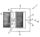
- the magnetic circuit 1 shown in the drawing comprises two half-circuits 2, 3, made of ferrite, in the shape of a "U".
- the ends of the legs of the half-circuits 2 and 3 are referenced 4, 5 and 6, 7 respectively.
- the ends 4 and 6 of the legs of the half-circuits 2, 3 must come into close contact with one another so as to leave only a very reduced air gap, the residual air gap having a thickness of less than 0.1 mm after assembly by gluing.
- the necessary air gap is created, by shortening, preferably by the same value, that is to say by the value of half the thickness of the air gap, the lengths of the legs having ends 5 and 7 (it is assumed that at the start the two legs of each "U" have the same length).
- the front faces of the ends 4 to 7 are rectified so that, on the one hand, the ends 4 and 6 allow a regular minimum residual air gap to persist, and so that the air gap of desired value is obtained between the ends 5 and 7.
- a wedge 8 of non-magnetic material is bonded between the ends 5 and 7, the thickness of which is practically equal to that of the desired air gap, taking into account the adhesive joint, this wedge only playing mechanical role.
- the shim 8 is made of magnetic material, with magnetic characteristics different from those of the half-circuits 2 and 3 and / or of section different from that of the legs of these circuits, in order to obtain other possibilities for adjusting the inductance values of the windings arranged on this magnetic circuit.
- a winding 9 with one or more windings (transformer or inductance) surrounds the ends 5 and 7 and the shim 8.
- the assembly of parts 2 and 3 and of the shim 8 is done using glue of the cold-bonding type with quick setting, making it possible to obtain joints with a thickness of less than 0.1 mm. You can also fix the winding carcass on the ends 5 and 7 with the same glue.
Description
La présente invention a pour objet un procéde de fabrication d'un circuit magnétique à faible champ magnétique rayonné, en particulier pour un transformateur haute tension alimentant un tube cathodique.The present invention relates to a method of manufacturing a magnetic circuit with a weak radiated magnetic field, in particular for a high-voltage transformer supplying a cathode-ray tube.
Les transformateurs haute tension tels que ceux utilisés pour alimenter des tubes cathodiques comportent généralement un entrefer de valeur bien déterminée dans leur circuit magnétique en ferrite. Cet entrefer rayonne un champ magnétique produisant des effets néfastes sur le tube cathodique, et même sur d'autres circuits pouvant les capter par effet d'antenne. On connaît d'après les documents FR-A-2 500 679 et DE-A-3 402 278 des circuits magnétiques pour bobinages, ces circuits magnétiques comportant au moins un entrefer épais, mais ces circuits connus nécessitent un réglage minutieux de l'épaisseur des entrefers lors de l'assemblage des transformateurs ou inducteurs montés sur ces circuits magnétiques.High-voltage transformers such as those used to supply cathode ray tubes generally have an air gap of well-defined value in their ferrite magnetic circuit. This air gap radiates a magnetic field producing harmful effects on the cathode ray tube, and even on other circuits which can pick them up by antenna effect. FR-A-2 500 679 and DE-A-3 402 278 disclose magnetic circuits for coils, these magnetic circuits comprising at least one thick air gap, but these known circuits require careful adjustment of the thickness air gaps during assembly of the transformers or inductors mounted on these magnetic circuits.
La présente invention a pour objet un procédé de fabrication d'un circuit magnétique pour transformateur haute tension dont les rayonnements produits par l'entrefer soient réduits à une valeur minimale et dont les effets sur les composants ou circuits environnants soient négligeables, ce circuit magnétique étant facile et peu onéreux à réaliser, en particulier pour une production en grande série, la valeur de l'inductance, et en particulier de l'inductance primaire du transformateur étant facile à ajuster avec de faibles tolérances.The subject of the present invention is a method of manufacturing a magnetic circuit for a high-voltage transformer whose radiation produced by the air gap is reduced to a minimum value and whose effects on the surrounding components or circuits are negligible, this magnetic circuit being easy and inexpensive to produce, in particular for mass production, the value of the inductance, and in particular of the primary inductance of the transformer, being easy to adjust with low tolerances.
Le procédé de fabrication d'un circuit magnétique conforme à l'invention, du type à deux demi-circuits en "U" est caractérisé par le fait que pour réduire le champ magnétique rayonné, la jambe logée à l'intérieur d'un bobinage comporte un entrefer usiné par rectification des extrémités des jambes correspondantes des demi-circuits, les extrémités des autres jambes des demi-circuits étant rectifiées et collées directement l'une sur l'autre.The method of manufacturing a magnetic circuit according to the invention, of the type with two half-circuits in a "U" shape, is characterized in that, in order to reduce the radiated magnetic field, the leg housed inside a coil has a machined air gap by rectifying the ends of the corresponding legs of the half-circuits, the ends of the other legs of the half-circuits being rectified and glued directly to each other.
La présente invention sera mieux comprise à la lecture de la description détaillée d'un mode de réalisation pris comme exemple non limitatif et illustré par le dessin annexé, dont la figure unique est une vue en coupe simplifiée d'un circuit magnétique conforme à l'invention.The present invention will be better understood on reading the detailed description of an embodiment taken as a nonlimiting example and illustrated by the appended drawing, the single figure of which is a simplified sectional view of a magnetic circuit according to invention.
Le circuit magnétique décrit ci-dessous est destiné à un transformateur haute tension alimentant un tube cathodique, mais il est bien entendu que l'invention n'est pas limitée à une telle application, et peut être utilisée aussi bien lorsque l'on désire réduire les rayonnements magnétiques d'un transformateur ou d'une inductance, que lorsque l'on désire régler à une valeur précise la valeur d'inductance d'un enroulement disposé sur un circuit magnétique.The magnetic circuit described below is intended for a high voltage transformer supplying a cathode ray tube, but it is understood that the invention is not limited to such an application, and can be used as well when it is desired to reduce magnetic radiation from a transformer or an inductance, only when it is desired to adjust the inductance value of a winding arranged on a magnetic circuit to a precise value.
Le circuit magnétique 1 représenté sur le dessin comporte deux demi-circuits 2, 3, en ferrite, en forme de "U". Les extrémités des jambes des demi-circuits 2 et 3 sont référencées 4, 5 et 6, 7 respectivement. Les extrémités 4 et 6 des jambes des demi-circuits 2, 3 doivent venir en contact étroit l'une contre l'autre pour ne laisser subsister qu'un entrefer très réduit, l'entrefer résiduel ayant une épaisseur inférieure à 0,1 mm après assemblage par collage.The
Entre les extrémités 5, 7, on crée l'entrefer nécessaire, en raccourcissant, de préférence de la même valeur, c'est-à-dire de la valeur de la moitié de l'épaisseur de l'entrefer, les longueurs des jambes ayant pour extrémités 5 et 7 (on suppose qu'au départ les deux jambes de chaque "U" ont la même longueur). Les faces frontales des extrémités 4 à 7 sont rectifiées pour que, d'une part les extrémités 4 et 6 laissent susbsister un entrefer résiduel minimal régulier, et pour que l'on obtienne entre les extrémités 5 et 7 l'entrefer de valeur désirée.Between the
Pour obtenir un assemblage solide, on colle entre les extrémités 5 et 7 une cale 8 en matériau amagnétique, dont l'épaisseur est pratiquement égale à celle de l'entrefer désiré, compte tenu du joint de colle, cette cale ne jouant qu'un rôle mécanique.To obtain a solid assembly, a wedge 8 of non-magnetic material is bonded between the
Selon une variante de l'invention, la cale 8 est en matériau magnétique, de caractéristiques magnétiques différentes de celles des demi-circuits 2 et 3 et/ou de section différente de celle des jambes de ces circuits, afin d'obtenir d'autres possibilités de réglage des valeurs d'inductance des enroulements disposés sur ce circuit magnétique. Un bobinage 9 à un ou plusieurs enroulements (transformateur ou inductance) entoure les extrémités 5 et 7 et la cale 8.According to a variant of the invention, the shim 8 is made of magnetic material, with magnetic characteristics different from those of the half-
De préférence, l'assemblage des parties 2 et 3 et de la cale 8 est fait à l'aide de colle du type à collage à froid avec prise rapide, permettant d'obtenir des joints d'épaisseur inférieure à 0,1 mm. On peut également fixer avec la même colle la carcasse du bobinage sur les extrémités 5 et 7.Preferably, the assembly of
Dans le cas de la réalisation d'un transformateur haute tension alimentant un tube cathodique, on a constaté que la valeur d'inductance du bobinage primaire d'un tel transformateur était critique, la tolérance devant être inférieure ou égale à 8 %, ce que l'on ne pouvait obtenir que difficilement avec les procédés de l'art antérieur, consistant à ajuster l'épaisseur de l'entrefer individuellement pour chaque transformateur.In the case of producing a high voltage transformer supplying a cathode ray tube, it has been found that the inductance value of the primary winding of such a transformer is critical, the tolerance having to be less than or equal to 8%, which it was difficult to obtain with the methods of the prior art, consisting in adjusting the thickness of the air gap individually for each transformer.
Par contre, selon la présente invention, il suffit, pour une même série de transformateurs ou d'inductances, d'usiner les jambes des demi-circuits 2 et 3 toujours aux mêmes longueurs, ces demi-circuits étant assemblés automatiquement avec la cale 8 et le bobinage 9, pour ne plus avoir à ajuster après assemblage l'épaisseur d'entrefer, en respectant facilement les tolérances fixées pour la valeur d'inductance.On the other hand, according to the present invention, it suffices, for the same series of transformers or inductors, to machine the legs of the half-
Par ailleurs, on a constaté une forte diminution du champ rayonné par le circuit de l'invention. On peut par exemple mesurer ce champ en un point 10 situé à une distance d (par exemple 1 cm) du circuit, sur le plan de joint des extrémités 4 et 6. Cette diminution peut être dans un rapport d'environ 3.Furthermore, there has been a sharp decrease in the field radiated by the circuit of the invention. One can for example measure this field at a
Claims (5)
- Method for manufacturing a magnetic circuit with a low radiated magnetic field, in particular for a high-voltage transformer supplying a cathode-ray tube, of the type with two "U-shaped" half-circuits (2, 3), characterised in that in order to reduce the radiated magnetic field, the limb (5, 7) housed inside a winding (9) includes an air gap machined by grinding the ends (5, 7) of the corresponding limbs of the half-circuits, the ends (4, 6) of the other limbs of the half-circuits being glued together directly.
- Method for manufacturing a magnetic circuit according to Claim 1, characterised in that the ends of the limbs of the two magnetic half-circuits are, on assembly, glued together, on the air gap side with the interposition of a block (8) with a thickness practically equal to the thickness of the desired air gap, and with a permeability less than that of the material of the magnetic circuit.
- Method for manufacturing a magnetic circuit according to Claim 2, characterised in that the block is made of a non-magnetic material.
- Method for manufacturing a magnetic circuit according to either of Claims 2 or 3, characterised in that the cross-section of the block is different from that of the limbs of the magnetic circuit.
- Method for manufacturing a magnetic circuit according to one of Claims 2 to 4, characterised in that a glue of the cold-bonding fast-setting type is used for the assembly.
Applications Claiming Priority (2)
| Application Number | Priority Date | Filing Date | Title |
|---|---|---|---|
| FR8517948A FR2591024B1 (en) | 1985-12-04 | 1985-12-04 | LOW MAGNETIC RADIUS MAGNETIC CIRCUIT, PARTICULARLY FOR A HIGH VOLTAGE TRANSFORMER SUPPLYING A CATHODE RAY TUBE |
| FR8517948 | 1985-12-04 |
Publications (2)
| Publication Number | Publication Date |
|---|---|
| EP0225830A1 EP0225830A1 (en) | 1987-06-16 |
| EP0225830B1 true EP0225830B1 (en) | 1993-03-31 |
Family
ID=9325439
Family Applications (1)
| Application Number | Title | Priority Date | Filing Date |
|---|---|---|---|
| EP86402674A Expired - Lifetime EP0225830B1 (en) | 1985-12-04 | 1986-12-02 | Method for producing a magnetic circuit with a low magnetic-leakage field, in particular for a high-voltage transformer supplying a cathode ray tube |
Country Status (6)
| Country | Link |
|---|---|
| EP (1) | EP0225830B1 (en) |
| JP (1) | JPS63502149A (en) |
| DE (1) | DE3688181T2 (en) |
| ES (1) | ES2039358T3 (en) |
| FR (1) | FR2591024B1 (en) |
| WO (1) | WO1987003736A1 (en) |
Cited By (3)
| Publication number | Priority date | Publication date | Assignee | Title |
|---|---|---|---|---|
| US8779885B2 (en) | 2002-12-13 | 2014-07-15 | Volterra Semiconductor Corporation | Method for making magnetic components with M-phase coupling, and related inductor structures |
| US8847722B2 (en) | 2002-12-13 | 2014-09-30 | Volterra Semiconductor Corporation | Method for making magnetic components with N-phase coupling, and related inductor structures |
| US9019063B2 (en) | 2009-08-10 | 2015-04-28 | Volterra Semiconductor Corporation | Coupled inductor with improved leakage inductance control |
Families Citing this family (10)
| Publication number | Priority date | Publication date | Assignee | Title |
|---|---|---|---|---|
| EP0471864B1 (en) * | 1990-08-17 | 1994-07-27 | TDK Corporation | Coil device |
| DE19528185A1 (en) * | 1995-08-01 | 1997-02-06 | Thomson Brandt Gmbh | transformer |
| US8237530B2 (en) | 2009-08-10 | 2012-08-07 | Volterra Semiconductor Corporation | Coupled inductor with improved leakage inductance control |
| US7965165B2 (en) | 2002-12-13 | 2011-06-21 | Volterra Semiconductor Corporation | Method for making magnetic components with M-phase coupling, and related inductor structures |
| US7352269B2 (en) | 2002-12-13 | 2008-04-01 | Volterra Semiconductor Corporation | Method for making magnetic components with N-phase coupling, and related inductor structures |
| US7498920B2 (en) | 2002-12-13 | 2009-03-03 | Volterra Semiconductor Corporation | Method for making magnetic components with N-phase coupling, and related inductor structures |
| US8102233B2 (en) | 2009-08-10 | 2012-01-24 | Volterra Semiconductor Corporation | Coupled inductor with improved leakage inductance control |
| JP2009064990A (en) * | 2007-09-07 | 2009-03-26 | Sht Corp Ltd | Coil unit |
| WO2009114872A1 (en) * | 2008-03-14 | 2009-09-17 | Volterra Semiconductor Corporation | Magnetic components with m-phase coupling, and related inductor structures |
| CN105719825A (en) * | 2016-01-22 | 2016-06-29 | 深圳顺络电子股份有限公司 | Inductor and fabrication method thereof |
Family Cites Families (6)
| Publication number | Priority date | Publication date | Assignee | Title |
|---|---|---|---|---|
| DE2927182C2 (en) * | 1979-07-05 | 1982-09-02 | Licentia Patent-Verwaltungs-Gmbh, 6000 Frankfurt | Method for producing a transformer, in particular a line transformer for a television receiver |
| DE3040368A1 (en) * | 1980-10-25 | 1982-05-27 | Vogt Gmbh & Co Kg, 8391 Erlau | Ferromagnetic core with filled air gap - uses lower permeability compacted iron powder in gaps of ferromagnetic cores |
| FR2500679A3 (en) * | 1981-02-20 | 1982-08-27 | Orega Cifte | Transformer mfg. method for line scan circuit of TV receiver - has gap of magnetic core adjusted by use of predetermined amount of hardening glue and coil impedance measurement |
| JPS5952812A (en) * | 1982-09-20 | 1984-03-27 | Matsushita Electric Ind Co Ltd | Fly-back transformer |
| JPS59168608A (en) * | 1983-03-14 | 1984-09-22 | Murata Mfg Co Ltd | Manufacture of fly-back transformer |
| DE3402278A1 (en) * | 1984-01-24 | 1985-08-01 | Vogt Gmbh & Co Kg, 8391 Erlau | Trimmable E-core for inductors |
-
1985
- 1985-12-04 FR FR8517948A patent/FR2591024B1/en not_active Expired
-
1986
- 1986-12-02 DE DE19863688181 patent/DE3688181T2/en not_active Expired - Fee Related
- 1986-12-02 ES ES86402674T patent/ES2039358T3/en not_active Expired - Lifetime
- 1986-12-02 JP JP50637886A patent/JPS63502149A/en active Pending
- 1986-12-02 EP EP86402674A patent/EP0225830B1/en not_active Expired - Lifetime
- 1986-12-02 WO PCT/FR1986/000412 patent/WO1987003736A1/en unknown
Non-Patent Citations (1)
| Title |
|---|
| Weichmagnetisches SIFERRIT -und SIRUFER-Material, Datenbuch 1975/1976, SIEMENS AG, page 59 * |
Cited By (7)
| Publication number | Priority date | Publication date | Assignee | Title |
|---|---|---|---|---|
| US8779885B2 (en) | 2002-12-13 | 2014-07-15 | Volterra Semiconductor Corporation | Method for making magnetic components with M-phase coupling, and related inductor structures |
| US8786395B2 (en) | 2002-12-13 | 2014-07-22 | Volterra Semiconductor Corporation | Method for making magnetic components with M-phase coupling, and related inductor structures |
| US8836461B2 (en) | 2002-12-13 | 2014-09-16 | Volterra Semiconductor Corporation | Method for making magnetic components with M-phase coupling, and related inductor structures |
| US8847722B2 (en) | 2002-12-13 | 2014-09-30 | Volterra Semiconductor Corporation | Method for making magnetic components with N-phase coupling, and related inductor structures |
| US9019064B2 (en) | 2002-12-13 | 2015-04-28 | Volterra Semiconductor Corporation | Method for making magnetic components with M-phase coupling, and related inductor structures |
| US9147515B2 (en) | 2002-12-13 | 2015-09-29 | Volterra Semiconductor LLC | Method for making magnetic components with M-phase coupling, and related inductor structures |
| US9019063B2 (en) | 2009-08-10 | 2015-04-28 | Volterra Semiconductor Corporation | Coupled inductor with improved leakage inductance control |
Also Published As
| Publication number | Publication date |
|---|---|
| DE3688181D1 (en) | 1993-05-06 |
| EP0225830A1 (en) | 1987-06-16 |
| DE3688181T2 (en) | 1993-07-08 |
| FR2591024A1 (en) | 1987-06-05 |
| WO1987003736A1 (en) | 1987-06-18 |
| FR2591024B1 (en) | 1988-01-08 |
| JPS63502149A (en) | 1988-08-18 |
| ES2039358T3 (en) | 1993-10-01 |
Similar Documents
| Publication | Publication Date | Title |
|---|---|---|
| EP0225830B1 (en) | Method for producing a magnetic circuit with a low magnetic-leakage field, in particular for a high-voltage transformer supplying a cathode ray tube | |
| EP0030186B1 (en) | Measuring shunt with induced error-voltage compensation | |
| EP0618568B1 (en) | Thin layer recording/reproducing magnetic head and production method | |
| FR2601218A1 (en) | SQUARE TRANSFORMER FOR HYBRID INTEGRATED CIRCUIT | |
| EP0313514A1 (en) | Manufacturing method of a non-slotted stator for an electric motor and electric motor fitted with such a stator | |
| EP0162766B1 (en) | High-energy and high-voltage storage device, and its use as a pulse generator | |
| EP1019926B1 (en) | Inductive component and method for making same | |
| EP0130902A2 (en) | Inductive electronic component for transmission by flat contacts | |
| FR2503505A1 (en) | CURRENT POWER SUPPLY SOURCE FOR A TELEVISION USING A MAGNETICABLE CORE ARRANGEMENT INTO TWO MATERIALS | |
| EP1063425A2 (en) | Ignition device for internal combustion engine | |
| EP0258362A1 (en) | High voltage transformer | |
| FR2721431A1 (en) | Automated mfg. process for transformer used in motor vehicle electronics | |
| EP0660339A1 (en) | Improvement relating to transformers of the closed ferrite magnetic circuit type | |
| EP0068946A1 (en) | Method of realising a unitary component consisting of an oscillating diode and a varactor diode, and frequency-tunable transmitter having such a unitary component | |
| US3686527A (en) | High-speed synthesized field focus coil | |
| EP0213982A1 (en) | Electronic inductive chip component, and method of making the same | |
| FR2681262A1 (en) | ACOUSTIC ELECTROMAGNETIC SOURCE OF PRESSURE PULSES. | |
| EP0280624A1 (en) | Device to position a magnetic circuit in relation to a coil of a high-tension transformer | |
| EP0442411B1 (en) | Conical spring for electric contact | |
| JP2000150244A (en) | Choke coil | |
| EP0543434B1 (en) | Magnetic head with a system of coils compensating magnetic leakage | |
| BE1002498A6 (en) | Manufacturing process of a magnetic core using a continuous metal ribbon | |
| FR3076391A1 (en) | INDUCTIVE FILTERING DEVICE WITH TORNE MAGNETIC CORE | |
| EP0033699B1 (en) | Method and device for assembling a magnetic circuit by using an adhesive | |
| FR3089367A1 (en) | AC / DC CONVERTER |
Legal Events
| Date | Code | Title | Description |
|---|---|---|---|
| PUAI | Public reference made under article 153(3) epc to a published international application that has entered the european phase |
Free format text: ORIGINAL CODE: 0009012 |
|
| AK | Designated contracting states |
Kind code of ref document: A1 Designated state(s): DE ES FR GB IT NL |
|
| 17P | Request for examination filed |
Effective date: 19871125 |
|
| 17Q | First examination report despatched |
Effective date: 19900618 |
|
| GRAA | (expected) grant |
Free format text: ORIGINAL CODE: 0009210 |
|
| AK | Designated contracting states |
Kind code of ref document: B1 Designated state(s): DE ES FR GB IT NL |
|
| ITF | It: translation for a ep patent filed |
Owner name: JACOBACCI CASETTA & PERANI S.P.A. |
|
| REF | Corresponds to: |
Ref document number: 3688181 Country of ref document: DE Date of ref document: 19930506 |
|
| GBT | Gb: translation of ep patent filed (gb section 77(6)(a)/1977) |
Effective date: 19930513 |
|
| REG | Reference to a national code |
Ref country code: ES Ref legal event code: FG2A Ref document number: 2039358 Country of ref document: ES Kind code of ref document: T3 |
|
| PGFP | Annual fee paid to national office [announced via postgrant information from national office to epo] |
Ref country code: GB Payment date: 19931119 Year of fee payment: 8 Ref country code: DE Payment date: 19931119 Year of fee payment: 8 |
|
| PGFP | Annual fee paid to national office [announced via postgrant information from national office to epo] |
Ref country code: ES Payment date: 19931213 Year of fee payment: 8 |
|
| PGFP | Annual fee paid to national office [announced via postgrant information from national office to epo] |
Ref country code: FR Payment date: 19931221 Year of fee payment: 8 |
|
| PGFP | Annual fee paid to national office [announced via postgrant information from national office to epo] |
Ref country code: NL Payment date: 19931231 Year of fee payment: 8 |
|
| PLBE | No opposition filed within time limit |
Free format text: ORIGINAL CODE: 0009261 |
|
| STAA | Information on the status of an ep patent application or granted ep patent |
Free format text: STATUS: NO OPPOSITION FILED WITHIN TIME LIMIT |
|
| 26N | No opposition filed | ||
| PG25 | Lapsed in a contracting state [announced via postgrant information from national office to epo] |
Ref country code: GB Effective date: 19941202 |
|
| PG25 | Lapsed in a contracting state [announced via postgrant information from national office to epo] |
Ref country code: ES Free format text: LAPSE BECAUSE OF THE APPLICANT RENOUNCES Effective date: 19941203 |
|
| PG25 | Lapsed in a contracting state [announced via postgrant information from national office to epo] |
Ref country code: NL Effective date: 19950701 |
|
| GBPC | Gb: european patent ceased through non-payment of renewal fee |
Effective date: 19941202 |
|
| PG25 | Lapsed in a contracting state [announced via postgrant information from national office to epo] |
Ref country code: FR Effective date: 19950831 |
|
| NLV4 | Nl: lapsed or anulled due to non-payment of the annual fee |
Effective date: 19950701 |
|
| PG25 | Lapsed in a contracting state [announced via postgrant information from national office to epo] |
Ref country code: DE Effective date: 19950901 |
|
| REG | Reference to a national code |
Ref country code: FR Ref legal event code: ST |
|
| REG | Reference to a national code |
Ref country code: ES Ref legal event code: FD2A Effective date: 20010402 |
|
| PG25 | Lapsed in a contracting state [announced via postgrant information from national office to epo] |
Ref country code: IT Free format text: LAPSE BECAUSE OF NON-PAYMENT OF DUE FEES;WARNING: LAPSES OF ITALIAN PATENTS WITH EFFECTIVE DATE BEFORE 2007 MAY HAVE OCCURRED AT ANY TIME BEFORE 2007. THE CORRECT EFFECTIVE DATE MAY BE DIFFERENT FROM THE ONE RECORDED. Effective date: 20051202 |