EP0220344A1 - Leistungsversorgung für Gasentladungseinrichtungen - Google Patents
Leistungsversorgung für Gasentladungseinrichtungen Download PDFInfo
- Publication number
- EP0220344A1 EP0220344A1 EP85307220A EP85307220A EP0220344A1 EP 0220344 A1 EP0220344 A1 EP 0220344A1 EP 85307220 A EP85307220 A EP 85307220A EP 85307220 A EP85307220 A EP 85307220A EP 0220344 A1 EP0220344 A1 EP 0220344A1
- Authority
- EP
- European Patent Office
- Prior art keywords
- transistor
- base
- supply circuit
- circuit according
- transformer
- Prior art date
- Legal status (The legal status is an assumption and is not a legal conclusion. Google has not performed a legal analysis and makes no representation as to the accuracy of the status listed.)
- Withdrawn
Links
Images

Classifications
-
- H—ELECTRICITY
- H02—GENERATION; CONVERSION OR DISTRIBUTION OF ELECTRIC POWER
- H02M—APPARATUS FOR CONVERSION BETWEEN AC AND AC, BETWEEN AC AND DC, OR BETWEEN DC AND DC, AND FOR USE WITH MAINS OR SIMILAR POWER SUPPLY SYSTEMS; CONVERSION OF DC OR AC INPUT POWER INTO SURGE OUTPUT POWER; CONTROL OR REGULATION THEREOF
- H02M3/00—Conversion of DC power input into DC power output
- H02M3/22—Conversion of DC power input into DC power output with intermediate conversion into AC
- H02M3/24—Conversion of DC power input into DC power output with intermediate conversion into AC by static converters
- H02M3/28—Conversion of DC power input into DC power output with intermediate conversion into AC by static converters using discharge tubes with control electrode or semiconductor devices with control electrode to produce the intermediate AC
- H02M3/325—Conversion of DC power input into DC power output with intermediate conversion into AC by static converters using discharge tubes with control electrode or semiconductor devices with control electrode to produce the intermediate AC using devices of a triode or a transistor type requiring continuous application of a control signal
- H02M3/335—Conversion of DC power input into DC power output with intermediate conversion into AC by static converters using discharge tubes with control electrode or semiconductor devices with control electrode to produce the intermediate AC using devices of a triode or a transistor type requiring continuous application of a control signal using semiconductor devices only
- H02M3/338—Conversion of DC power input into DC power output with intermediate conversion into AC by static converters using discharge tubes with control electrode or semiconductor devices with control electrode to produce the intermediate AC using devices of a triode or a transistor type requiring continuous application of a control signal using semiconductor devices only in a self-oscillating arrangement
Definitions
- This invention relates to a low current, high voltage power supply for neon signs or other similar gas discharge devices and in particular to a solid state power supply which is far more efficient and less costly than conventional high voltage transformers used to excite gas discharge devices.
- Gas discharge devices such as tubes for neon signs, require a high voltage, typically between five to ten thousand volts or more, to stimulate the gas atoms therein sufficiently to emit radiation in the visible spectrum.
- a high voltage typically between five to ten thousand volts or more
- such high voltages are generally produced by a low frequency step-up transformer connected to a standard 60 Hz power line.
- the resulting transformers are expensive, heavy and generally bulky.
- the power supply of the invention utilizes a unique solid state free-running power oscillator to generate a high frequency power signal which drives a compact, light-weight high frequency transformer.
- the transformer delivers a sufficiently high voltage to excite the inert gas within a gas-filled tube in order to cause it to produce light. In this manner, the conventional bulky, low frequency step-up transformer is eliminated.
- the transformer is of the type having leakage reactance. It has a primary winding, a feedback winding, and a secondary winding connected to the gas-filled tube.
- a transistor is employed, having its collector connected to the transformer primary winding and its base connected to the transformer feedback winding to provide a base current drive. When voltage is applied to the base of the transistor, the transistor conducts until the transistor comes out of saturation from increasing collector current.
- a solid state switch is connected to the primary winding and is activated when the transistor comes out of saturation in order to remove the base drive to render the transistor non-conductive. The switch also provides a path for rapid evacuation of charge carriers stored in the base-emitter junction of the transistor to rapidly render the transistor non-conductive.
- the switch comprises a second transistor having its base connected to the transformer primary winding and its collector connected to the base of the first transistor in order to provide the rapid evacuation path for the base-emitter junction of the first transistor.
- the emitter of the second transistor is directly grounded.
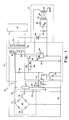
- the neon sign supply of the invention is shown generally at 10 in Figure 1.
- the supply 10 includes a power supply 12, a start-up circuit 14, a high frequency oscillator 16 connected to an output load 18, typically a neon tube or other similar device and a safety bypass circuit 17.
- the power supply 12 consists of a bridge rectifier 20 and a filter capacitor 22.
- the rectifier 20 is connected to a conventional 120 volt alternating current supply (not illustrated) through leads 24 and 26.
- the positive output of the power supply 12 is directed on line 28 to the start-up circuit 14 and the oscillator 16, while the negative output of the power supply 12 is connected to "ground" 30 of the neon supply 10.
- the start-up circuit 14 consists of the parallel combination of a capacitor 32 and resistor 34 connected at one end to the line 28 and at the other end in series with a resistor 36.
- the resistor 36 is connected through the parallel combination of a charging capacitor 38 and resistor 39 to the ground 30. It is also connected to a diac 40 in series with a current limiting resistor 42 on a line 44 leading to the oscillator 16.
- the start-up circuit 14 operates as a relaxation oscillator in which the capacitor 38 is charged until the voltage across the capacitor 38 exceeds the threshold trigger voltage of the diac 40. The diac 40 then conducts, and when the current through the diac 40 has substantially stopped due to completion of the charge on the capacitor 38, the diac switches off, commencing a new and repetitive charge cycle. If the oscillator 16 is not previously in oscillation, the repetitive discharge cycles of the diac 40 initiate such oscillation.
- the frequency of oscillation of the start-up circuit 14 is not critical, generally and preferrably having a period initially of 200 Hz and later settling to a steady state of 10 to 20 Hz.
- the oscillator 16 is a free-running high frequency oscillator comprising a power transistor 46, a low voltage switch transistor 48, an output and feedback transformer 50, and associated biasing and triggering circuit elements. It is preferred that the oscillator 16 nominally operate under load at a frequency of 25 KHz.
- the power transistor 46 is of a common type having a collector-emitter breakdown voltage rating of approximately 1500 volts and a maximum collector current nominally of 2.5 amperes. Such a transistor is commonly found in a television horizontal output circuit, and transistors having a collector current between two and seven amperes are suitable in this invention.
- the collector of the transistor 46 is connected to the positive output line 28 of the power supply 12 through the primary 52 of the transformer 50.
- the base of the transistor 46 is connected through a biasing network 54 and a diode 56 to a transformer feedback winding 58, while the emitter of the transistor 46 is connected to ground through an emitter biasing network 60.
- the emitter biasing network 60 comprises the parallel combination of a resistor 62 and a by-pass capacitor 64.
- the capacitor 64 functions as a low impedance by-pass capacitor at the frequency of oscillation of the network 60, thereby producing a substantially constant direct current voltage at the emitter of the transistor 46.
- the resistor 62 can be replaced by a positive temperature coeffient resistance element which increases in resistance as voltage across the element increases, such as a standard incandescent lamp. Substituting such a device for the resistor 62 permits the potential across the emitter bias network 60 to be varied as necessary to compensate for changing load and temperature conditions.
- the base bias network 54 is connected to the base of the transistor 46 and comprises the parallel combination of a by-pass capacitor 66 and a resistor 68. Similar to the biasing network 60, the resistor 68 may be replaced by an incandescent lamp to permit variance of the potential across the biasing network 54 as necessary. In addition, the resistor 68 can be replaced by a variable resistor or may be used in series with a variable resistor in order to set the quiescent biasing level of the transistor 46.
- the transformer 50 includes the primary 52, the feedback winding 58 and a secondary winding 70.
- the transformer is preferrably formed such that the windings 52, 58 and 70 are provided on a generally rectangular ferrite core comprised of two opposed U-shaped pieces formed to create a 0.05 inch air gap between respective adjacent ends of the U-shaped core members.
- the number of turns of each of the windings is set forth below in a table illustrating representative values of the various elements of the neon supply 10.
- the number of turns in the primary 52 is set, and the air gap is adjusted large enough to avoid core saturation and to establish a given inductance in the primary winding 52 which, in turn, establishes the frequency of oscillation of the oscillator 16, in conjunction with capacitor 72.
- the secondary-to-primary turns ratio is selected according to conventional transformer relationships to provide the requisite output voltage to excite the output load 18.
- Neon and other similar gas discharge tubes are known to possess a highly non-linear voltage-current characteristic wherein substantially no current passes through the tube until the threshold excitation voltage is achieved and, thereafter, substantial and excessive currents may result unless means for limiting such current are provided.
- a pure "constant voltage" power source without current limiting is unsatisfactory for use with gas discharge tubes.
- the geometry of the transformer 50 may be designed to provide the voltage source of this invention with inherent current limiting which functions, in essence, as a constant current source under the low load resistance presented by an excited gas discharge tube.
- This feature is achieved in a conventional manner by positioning the primary 52 and secondary 70 windings on different poles of the transformer core thereby producing a leakage reactance between these windings.
- the maximum current is limited by this leakage reactance.
- the feedback winding 58 of the transformer 50 is connected through the diode 56 and the bias network 54 to the base of the transistor 46. As seen, the feedback winding 58 is also connected through the diode 56 to the collector of the transistor 48, for reasons described in greater detail below.
- the number of turns of the feedback winding 58 is selected to assure adequate feedback for oscillation and, more particularly, to force the transistor 46 into saturation over a substantial portion of each cycle as required to produce sufficient power output to drive the load 18.
- the diode 56 is positioned between the feedback winding 58 and the base bias network 54 in such polarity to generally block the reverse flow of current through the winding 58.
- the diode 26 preferrably is a fast recovery type of diode to prevent an instantaneous reverse current from flowing following initial reverse biasing of the diode.
- the primary winding 52 is connected to the base of the transistor 48 through a blocking and primary resonating capacitor 72.
- a resistor 74 and diode 76 are also attached to the base of the transistor 48, and the emitter of the transistor 48 is connected to the ground 30.
- the diode 76 is a clamping diode which limits the maximum base-to-emitter voltage of the transistor 48 to assure that the emitter-base breakdown voltage of the transistor 48 is not exceeded.
- the resistor 74 is connected in parallel with the diode 76 to provide a low impedance path effectively across the emitter-base junction of the transistor 48, thereby shunting, in a conventional manner, the collector-to-emitter leakage current of the transistor 48.
- the purpose of the transistor 48 is to aid in rapid turn-off of the transistor 46.
- charge carriers stored in the base-emitter junction of the transistor 46 normally remain, and are recombined in a natural recombination process. This recombination process results in a substantial turn-off delay and therefore gradual and dissipative turn-off of the transistor 46.
- the transistor 48 being biased to conduct at the instant of desired turn-off of the transistor 46, the charge carriers stored in the base-emitter junction of the transistor 46 are rapidly evacuated through base-emitter reverse bias from the biasing network 54 and the conducting transistor 48.
- the rapid evacuation of the base-emitter junction of the transistor 46 occurs in a time period much shorter than that required for the natural recombination process, aiding the rapid turn-off of the transistor 46.
- the safety bypass curcuit 17 causes the remainder of the supply 10 to revert to a low energy pulse mode which prevents any ensuing burns or a fire.
- the secondary winding 88 of the transformer 84 is connected to a diode 90 whose output is directed to a filter capacitor tor 94, and the gate cathode of a triac or silicon controlled rectifier 96.
- a triac is preferred.
- the triac 96 is connected to the feedback winding 58 of the transformer 50 and to the ground 30.
- the start-up circuit 14 When connected, line voltage on the leads 24 and 26 is rectified by the bridge 20 and appears across the capacitor 22.
- the start-up circuit 14 generates a series of pulses to initiate oscillation of the oscillator 16.
- the start-up circuit Preferably, the start-up circuit generates pulses at a frequency of 200 Hz, settling to a steady-state pulse generation of between 10 and 20 Hz.
- the pulses of the start-up circuit 14 have a negligible effect and may continue without altering oscillation of the oscillator 16.
- the collector voltage V C begins to rise rapidly as the current I L begins to drop, and the negative base current I B begins to diminish. Since the transistor 46 remains in a non-conducting state, as the current I L continues to decrease, the collector voltage V C of the transistor 46 reaches a maximum at time T3, at which time the collector voltage begins to decrease. At the same time, the sign of dVc/ dt changes, reversing current through the transistor 48 emitter-base junction, causing the transistor 48 to cease conducting. The current I L in the primary 52 then goes negative, and the collector voltage V C of the transistor 46 decreases to zero, as the reverse current in the primary 52 reaches its maximum negative value.
- the osillator 16 is halted, it is not restarted until another pulse is received from the diac 40, a period of several hundred milliseconds. If the fault condition across the secondary winding 70 has not cleared, a new pulse from the diac 40 only causes a new fault current, thus repeating the above sequence of initiation of the safety bypass circuit 17. The resulting continual repetition of activation of the safety bypass circuit 17 prevents any significant power output level of the transformer 50.
- the output voltage of the transformer 60 can be altered in a well-known manner.
Landscapes
- Engineering & Computer Science (AREA)
- Power Engineering (AREA)
- Circuit Arrangements For Discharge Lamps (AREA)
Applications Claiming Priority (1)
| Application Number | Priority Date | Filing Date | Title |
|---|---|---|---|
| US59086884A | 1984-03-19 | 1984-03-19 |
Publications (1)
| Publication Number | Publication Date |
|---|---|
| EP0220344A1 true EP0220344A1 (de) | 1987-05-06 |
Family
ID=24364059
Family Applications (1)
| Application Number | Title | Priority Date | Filing Date |
|---|---|---|---|
| EP85307220A Withdrawn EP0220344A1 (de) | 1984-03-19 | 1985-10-09 | Leistungsversorgung für Gasentladungseinrichtungen |
Country Status (1)
| Country | Link |
|---|---|
| EP (1) | EP0220344A1 (de) |
Citations (4)
| Publication number | Priority date | Publication date | Assignee | Title |
|---|---|---|---|---|
| FR95960E (fr) * | 1968-09-13 | 1972-05-19 | Radiotechnique Compelec | Perfectionnements aux dispositifs d'allumage électronique pour moteur a combustion interne. |
| GB2018529A (en) * | 1978-04-06 | 1979-10-17 | Westfaelische Metall Industrie | DC-to-DC converters |
| FR2469857A1 (fr) * | 1979-11-07 | 1981-05-22 | Fuji Koeki Corp | Dispositif electrique producteur d'eclairs lumineux |
| US4451772A (en) * | 1982-09-09 | 1984-05-29 | Eastman Kodak Company | Passive clamp for on/off control of a capacitor charger |
-
1985
- 1985-10-09 EP EP85307220A patent/EP0220344A1/de not_active Withdrawn
Patent Citations (4)
| Publication number | Priority date | Publication date | Assignee | Title |
|---|---|---|---|---|
| FR95960E (fr) * | 1968-09-13 | 1972-05-19 | Radiotechnique Compelec | Perfectionnements aux dispositifs d'allumage électronique pour moteur a combustion interne. |
| GB2018529A (en) * | 1978-04-06 | 1979-10-17 | Westfaelische Metall Industrie | DC-to-DC converters |
| FR2469857A1 (fr) * | 1979-11-07 | 1981-05-22 | Fuji Koeki Corp | Dispositif electrique producteur d'eclairs lumineux |
| US4451772A (en) * | 1982-09-09 | 1984-05-29 | Eastman Kodak Company | Passive clamp for on/off control of a capacitor charger |
Similar Documents
| Publication | Publication Date | Title |
|---|---|---|
| US4613934A (en) | Power supply for gas discharge devices | |
| US4060751A (en) | Dual mode solid state inverter circuit for starting and ballasting gas discharge lamps | |
| CA2012929C (en) | Lamp starting circuit | |
| US3917976A (en) | Starting and operating circuit for gaseous discharge lamps | |
| US3334270A (en) | Discharge lamp circuit | |
| US4000443A (en) | Voltage control | |
| US4503362A (en) | Frequency stabilized, gain controlled ballast system | |
| GB1570926A (en) | Circuit for starting and operating gas discharge lamp | |
| US4392081A (en) | Lighting unit | |
| USRE32904E (en) | Power supply for gas discharge devices | |
| US4959593A (en) | Two-lead igniter for HID lamps | |
| EP0031933B1 (de) | Betriebsschaltung niedriger Spannung für Fluoreszenzlampen | |
| US4013921A (en) | Warning light control | |
| CA1086815A (en) | High frequency transistor ballast | |
| CA1101487A (en) | Trigger circuit for flash lamp directly coupled to ac source | |
| US3544840A (en) | Voltage multiplier power supply for gas-discharge lamps | |
| US5572093A (en) | Regulation of hot restrike pulse intensity and repetition | |
| EP0220344A1 (de) | Leistungsversorgung für Gasentladungseinrichtungen | |
| US3949273A (en) | Burner ignition system | |
| US4069442A (en) | Pulse circuit for gaseous discharge lamps | |
| CA1258137A (en) | Power supply for gas discharge devices | |
| ES8402688A1 (es) | Aparato del tipo de reactancia auxiliar para hacer funcionar lamparas de descarga con energia de corriente alterna. | |
| CA1263433A (en) | Apparatus for starting and operating a discharge lamp | |
| US3307098A (en) | Inverter having a single selfcommutating thyristor | |
| US3524102A (en) | Solid state means for gas discharge lamp |
Legal Events
| Date | Code | Title | Description |
|---|---|---|---|
| PUAI | Public reference made under article 153(3) epc to a published international application that has entered the european phase |
Free format text: ORIGINAL CODE: 0009012 |
|
| AK | Designated contracting states |
Kind code of ref document: A1 Designated state(s): AT BE CH DE FR GB IT LI NL SE |
|
| 17P | Request for examination filed |
Effective date: 19871020 |
|
| 17Q | First examination report despatched |
Effective date: 19891120 |
|
| STAA | Information on the status of an ep patent application or granted ep patent |
Free format text: STATUS: THE APPLICATION IS DEEMED TO BE WITHDRAWN |
|
| 18D | Application deemed to be withdrawn |
Effective date: 19901219 |