EP0216580B1 - Infinite impulse response filters - Google Patents
Infinite impulse response filters Download PDFInfo
- Publication number
- EP0216580B1 EP0216580B1 EP86307025A EP86307025A EP0216580B1 EP 0216580 B1 EP0216580 B1 EP 0216580B1 EP 86307025 A EP86307025 A EP 86307025A EP 86307025 A EP86307025 A EP 86307025A EP 0216580 B1 EP0216580 B1 EP 0216580B1
- Authority
- EP
- European Patent Office
- Prior art keywords
- filter
- output
- words
- iir
- iir filter
- Prior art date
- Legal status (The legal status is an assumption and is not a legal conclusion. Google has not performed a legal analysis and makes no representation as to the accuracy of the status listed.)
- Expired - Lifetime
Links
Images
Classifications
-
- H—ELECTRICITY
- H03—ELECTRONIC CIRCUITRY
- H03H—IMPEDANCE NETWORKS, e.g. RESONANT CIRCUITS; RESONATORS
- H03H17/00—Networks using digital techniques
- H03H17/02—Frequency selective networks
- H03H17/04—Recursive filters
Definitions
- This invention relates to infinite impulse response (IIR) filters.
- an IIR filter is a type of digital filter which can be used to effect filtration of an input signal that comprises a sequence of digital words (which may, for example, comprise samples of an analog signal) spaced in time by an interval T.
- the filter is operative during each of a plurality of periods of time (clock periods) equal to T to process sets of relatively delayed words of the input signal to produce a word of a filtered output signal.
- the IIR filter is distinguished from some other types of digital filter in that it is recursive. That is to say, each output word (or sample) is a function of a past or previously generated word or words as well as of present and past input words.
- the IIR filter includes a feedback loop which feeds back at least one word to adding means where it is summed with other signals.
- the word that is fed back is multiplied by a weighting coefficient.
- an infinite impulse response filter for filtering an input signal that comprises a sequence of digital words spaced in time by an interval T, the filter comprising: p IIR filter portions all connected to receive all the words of the input signal, each filter portion being operative during each of a plurality of periods of time equal to p.T to produce an output word by combining a respective set of adjacent words of the input signal and an output word produced by that filter portion during a previous said period of time, the sets of adjacent words of the input signal combined by each of the p IIR filter portions during each said period of time being offset with respect to one another by one word; and means for multiplexing together the p output words produced during each said period of time to constitute a filtered output signal comprising a sequence of said output words spaced in time by the interval T.
- the p IIR filter portions are operative to produce p output words during periods of time equal to p.T, that is, each of them can operate at a data rate equal to the data rate of the input signal divided by p, the time available to form each output word is increased (as compared to the above-described conventional filter) by a factor equal to p. Accordingly, if processing components (multipliers and adders) having the same operating speeds are used, the maximum operating speed of the present IIR filter is increased by a factor of p relative to the above-described conventional type of IIR filter.
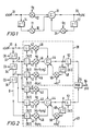
- Equations (1) and (2) can be implemented in hardware terms by the structure shown in Figure 1.
- the input signal x(n), whose z-transform is X(z), is supplied to an input terminal or port 10.
- the input signal is a sequence of digital words (for example, but not necessarily, 8-bit words) having the spacing T.
- the input signal is passed to a multiplier 12 where each successive word is multiplied by the weighting coefficient a0.
- the input signal is passed also to a Z ⁇ 1 delay element 14 in which it is subjected to a delay equal to T, namely a one word or sampling period delay.
- the output signal produced by the delay element 14 is passed to a multiplier 16 where each successive word thereof is multiplied by the weighting coefficient a1.
- each output word is a function of a past or previously generated word or words as well as present and past input words or samples.
- the filter of Figure 1 includes a feedback loop, connected between the output of the adder 18 and another input of the adder, the adder being operative to sum an output word sent back via the feedback loop with the words from the multipliers 12 and 16.
- the feedback loop comprises a Z ⁇ 1 delay element 22 (delay time T) and a multiplier 24 in which the output signal from the delay element 22 is multiplied by the weighting coefficient -b1.
- the value +b1 (rather than -b1) can instead be applied to the multiplier 24 if the adder is configured to perform an addition operation in which its inputs from the multipliers 12 and 16 are considered positive while its input from the multiplier 24 is considered negative).
- Faster signals can be handled only by increasing the speed of the multiplier and/or adder, which may be difficult and/or excessively expensive and/or impossible.
- Equation (1) it will be seen from a comparison of Equation (1) with the circuit of Figure 1 that the denominator of Equation (1) is representative mathematically of the feedback loop of Figure 1. Therefore, if it is possible to implement an IIR filter circuit which is generally similar to that of Figure 1, but which operates in accordance with Equation (5), then since the denominator contains a term which is a function of Z ⁇ 2 (but not a term which is a function of Z ⁇ 1) it should be possible to double the time available for forming each output word. Therefore, for a multiplier and adder operating at the same speeds, the maximum operating speed of the filter also will be doubled.
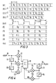
- the IIR filter shown in Figure 2 comprises an input terminal or port 30 to which an input signal x(n) is applied.
- the input signal x(n) comprises a stream or sequence of digital words or samples spaced in time b) the interval (sampling internal) T.
- the input signal, as present at a point A in Figure 2, is shown in Figure 3(A). It comprises a sequence of words X ⁇ 2, X ⁇ 1, X0, X1, X2 etc.
- the input signal is directed through a delay means comprising three Z ⁇ 1 delay elements 32, 34, 36 connected in cascade or tandem so as successively to delay it by increments of time equal to T.
- a delay means comprising three Z ⁇ 1 delay elements 32, 34, 36 connected in cascade or tandem so as successively to delay it by increments of time equal to T.
- Two IIR processing units 38, 40 are connected to receive respective groups of the series of four relatively delayed signals available at the points A to D. Specifically, the unit 38 receives the group of signals at the points A to C and the unit 40 receives the group of signals at the points B to D, the two groups thus being offset with respect to one another by one word.
- the two IIR processing units 38, 40 are preferably, as shown, of substantially identical construction.
- Each unit comprises three latches 42, each having a bit capacity appropriate to the number of bits in each word of the input signal, so as to latch into each unit 38,40 under the control of a clock signal CK/2 ( Figure 3), words from the appropriate group (A to C or B to D) of the series of four relatively delayed signals.
- the outputs of the latches 24 are connected to respective inputs of an adder 44 via respective multipliers 46 having weighting coefficients a o , (a1 -b1 a o ) and -b1 a1 which correspond to those in the numerator of Equation (4) above.
- each adder 44 is connected back to a further input of the adder via a feedback loop comprising a delay element 48 and a multiplier 50.
- the delay element 48 is a Z ⁇ 2 delay element and therefore produces a delay of 2T.
- the weighting coefficient of the multiplier 50 is +b12, which is that appearing in the final term of the difference equation, namely Equation (6).
- the outputs of the adders 44 are connected via respective latches 52 (supplied with the clock signal CK/2) to respective inputs of a multiplexer 54 which has an output terminal or port 56 at which the filtered output signal y(n) of the filter is produced.
- the clock signal CK/2 which is supplied to the latches 42, 52 and other components of the processing units 38, 40, has a frequency that is half the frequency or data rate fs of the input signal. That is, the period of the clock signal CK/2 is equal to 2T. Accordingly, in order that the delay elements 32, 34, 36 will produce delays of Z ⁇ 1, they are supplied with a clock signal CK having a frequency (equal to fs) that is twice that of the clock signal CK/2.
- the delay elements 32, 34, 36 can in fact be of the same construction as the latches 42, 52, which are used to pipeline the various signals through the processing units 38, 40, the sole functional difference between them being that they are supplied with clock signals (CK and CK/2, respectivey) of different frequencies.
- the latches 42 serve effectively to demultiplex the input signal so that, during each of the clock periods (2T) of the clock signal CK/2, the processing units 38, 40 can process simultaneously or contemporaneously, that is in parallel, respective sets of words of the input signal which are offset by one word and which, in the conventional IIR filter of Figure 1, have to be processed (at twice the speed) during successive clock periods equal to T.
- This effective halving of the data rate of the processing units 38, 40 which is achievable by virtue of the fact that it implements Equation (5) which has no term for Z ⁇ 1 in its denominator (feedback loop), is what enables relaxation of the constraint on the maximum operating speed of the filter to be achieved.
- the clock signal CK/2 is depicted in Figure 3 as comprising a series of clock pulses. As explained above, it has a period equal to 2T and therefore has a frequency which is half the data rate fs of the input signal. As represented by the arrows in Figure 3, the clock signal becomes effective upon the latches 42 (and the other circuits to which it is connected) at the leading edges of the clock pulses thereof. Assume that, just prior to one such edge occurring at a time t o , the words X o , X ⁇ 1 and X ⁇ 2 are stored in the latches 42 of the unit 38 and the words X ⁇ 1, X ⁇ 2 and X ⁇ 3 are stored in the latches 42 of the unit 40.
- the processing unit 38 produces an output word Y o ( Figure 3(F)) which is based upon the set of input words X o , X ⁇ 1 and X ⁇ 2 and which conforms to Equation (5).
- the processing unit 40 produces an output word Y ⁇ 1 ( Figure 3(H)) which is based upon the set of input words X ⁇ 1, X ⁇ 2 and X ⁇ 3 and which also conforms to Equation (4).
- the components of the processing units have twice as much time to carry out their operations than is the case for the conventional circuit of Figure 1 where the two words are produced successively in consecutive clock periods equal to T.
- the reduction in speed is achievable by virtue of the fact that the feedback loop does not need to incorporate a Z ⁇ 1 delay element but, in this embodiment, comprises a single Z ⁇ 2 delay element 48.
- the Z ⁇ 2 delay element 48 may comprise a latch similar to the latches 42, 52 and supplied with the same clock signal CK/2).
- the output words Y o and Y ⁇ 1 produced by the processing units 38,40, respectively, are passed via the latches 52 to the multiplexer 54 where they are multiplexed together in the proper order, at the full data rate fs, to produce the output word sequence y(n): see Figure 3.
- the filter of Figure 2 effectively filters the input signal in the same way as that of Figure 1, that is it has the same transfer response, but it does so by processing pairs of words in parallel (at a reduced rate) rather than by processing sets of words serially (at the full rate).
- the IIR filter of Figure 2 displays the advantage that it has twice as much time available to produce each output word than does the conventional IIR filter of Figure 1 so that, for the same operating times of the relevant circuit components, the maximum signal frequency or data rate that it can handle is doubled.
- the same technique can be extended to higher values of p (probably only corresponding to integral powers of 2).
- the numerator Y(z) of the transfer characteristic equation would become much more complex in order to obtain the same filter response.
- the transfer characteristic of a two-pole (second order) IIR filter can be represented by the equation: where a2 and b2 represent further constants (weighting coefficients) and the other symbols are as defined above.
- Equations (7) and (8) can be implemented in hardware terms is shown in Figure 4. This structure is similar in many respects to that of Figure 1 and will be described only in so far as it differs from that of Figure 1.
- components which are the same as or similar to components of the filter of Figure 1 are represented by the same references.
- Equation (9) which are a function of Z ⁇ 1 and Z ⁇ 3 cancel out, leaving only unity and functions of Z ⁇ 2 and Z ⁇ 4.
- Equation (10) can be implemented in hardware terms in such a manner that the feedback loop contains only functions of Z ⁇ 2 and Z ⁇ 4 (in practice implemented as two Z ⁇ 2 delay elements connected in cascade), the implementation being a demultiplexed version of Figure 4 running at half the data rate in like manner to that in which the one-pole implementation of Figure 2 is a demultiplexed version of Figure 1 running at half the data rate.
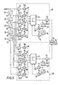
- Equations (10) and (11) can be implemented is shown in Figure 5.
- the structure of Figure 5 is similar in many respects to that of Figure 2 and will only be described in so far as it differs from that of Figure 2.
- components which are the same as or similar to components of the filter of Figure 2 are represented by the same references.
- the filter of Figure 5 functions in a manner very similar to that of Figure 2 to replicate the response of the conventional two-pole filter of Figure 4, but in such a manner that, during each clock period equal to 2T, a pair of sets of words are processed in parallel (at a halved data rate) instead of such pair being processed consecutively (at the full data rate) in respective consecutive clock periods equal to T.
- the filter of Figure 5 displays the same advantage over that of Figure 4 that the filter of Figure 2 displays over that of Figure 1, namely it has twice as much time to generate output signal words as does the filter of Figure 4 so that, for the same operating times of the relevant circuit components, the maximum input signal frequency or data rate that it can handle is doubled.
- the principle underlying the design of the filter of Figure 5 can be extended to provide filters running p times (where p is greater than 2 and probably is an integral power of 2) more slowly than the full (input) data rate.
- the denominator X(z) of the transfer characteristic equation governing the operation of the filter might be reduced to functions of Z ⁇ 4 and Z ⁇ 8 (or Z ⁇ 8, Z ⁇ 16 etc.), in which case the data rate would be reduced by a factor of 4 (8, etc.) and 4 (8, etc.) processing units would be employed to process 4 (8, etc.) of input words in parallel or contemporaneously.
- the denominator X(z) can be made a function of Z which is of order 2p so as to contain terms for Z which are powers of -p and -2p. Obviously, however, for higher values of p than Z the numerator of the equation would become much more complex in order to obtain the same filter response.
- each of the IIR processing units 38, 40 in conjunction with a respective part of the delay means 32,34,36 or 32,34,36,70,72, constitutes a respective demultiplexed IIR filter or filter portion that implements Equation (5) or Equation (10), but with the groups of adjacent words processed by the two units being offset with respect to one another by one word.
- the processing unit 38 and the delay elements 32,34 form one IIR filter portion and the processing unit 40 and the delay elements 32,34,36 form the other IIR filter portion.
- the delay means is shared between the IIR filter portions to provide hardware economy, because incorporating a separate delay means in each IIR filter portion would increase the number of delay elements in that, in Figure 2, the three delay elements 32,34,36 would have to be replaced by five elements (two in the unit 38 and three in the unit 40) and, in Figure 5, the five delay elements 32,34,36,70,72 would have to be replaced by nine elements (four in the unit 38 and five in the unit 40). Nonetheless, it should be appreciated that the IIR processing units 38,40 and the shared delay means could be replaced by respective IIR filter portions including respective individual delay means. Such an arrangement may in fact be considered preferable in some cases in that it may enable the filter to be implemented in hardware terms as two or more substantially identical portions which might be formed as respective substantially identical circuit assemblies such as circuit boards.
- the invention can be embodied in other ways than those described above with reference to Figures 2 and 5.
- the circuits as shown in Figures 2 and 5 can be transformed into alternative structures by using a transposition (flow graph reversal) technique: see "Digital Signal Processing", A.V. Oppenheim and R.W. Schafer, Prentice-Hall, Inc., 1975 at pages 130 to 160.
- transposition flow graph reversal
- alternative structures obtained by transposition will be of substantially different form than the structures shown in Figures 2 and 5, they will function equivalently and have the same transfer characteristics of the structures of Figures 2 and 5.
- Equation (7) can be implemented in other forms than that shown in Figure 4.
- a filter embodying the invention can be designed by the following technique.
- a basic or non-demultiplexed form is chosen and a desired response of the filter is selected by calculating suitable values for the weighting coefficients of the transfer characteristic equation of the basic or non-demultiplexed form.
- the modified equation corresponds to a demultiplexed filter or filter portion having an order m.p (where m is the order of the basic or non-demultiplexed form of the filter).
- the modified equation is then implemented in any desired way to form art IIR filter portion or to form an IIR processing unit that shares its delay means with its (p-1) counterparts.
- the same implementation is used for each of the p processing units or filter portions so that they will all be of substantially identical construction.
- the modified equation could be implemented in more than one way so as to form processing units or filter portions of different constructions.
- a multiplexer is then associated with the p filter portions (that is p separate filter portions or p processing units sharing a common delay means) to form the complete demultiplexed filter.
Landscapes
- Physics & Mathematics (AREA)
- Engineering & Computer Science (AREA)
- Computer Hardware Design (AREA)
- Mathematical Physics (AREA)
- Complex Calculations (AREA)
- Networks Using Active Elements (AREA)
- Control Of Motors That Do Not Use Commutators (AREA)
- Input Circuits Of Receivers And Coupling Of Receivers And Audio Equipment (AREA)
- Filters That Use Time-Delay Elements (AREA)
- Analogue/Digital Conversion (AREA)
- Electrophonic Musical Instruments (AREA)
Abstract
Description
- This invention relates to infinite impulse response (IIR) filters.
- As is known to those skilled in the art, an IIR filter is a type of digital filter which can be used to effect filtration of an input signal that comprises a sequence of digital words (which may, for example, comprise samples of an analog signal) spaced in time by an interval T. The filter is operative during each of a plurality of periods of time (clock periods) equal to T to process sets of relatively delayed words of the input signal to produce a word of a filtered output signal. The IIR filter is distinguished from some other types of digital filter in that it is recursive. That is to say, each output word (or sample) is a function of a past or previously generated word or words as well as of present and past input words. Accordingly, the IIR filter includes a feedback loop which feeds back at least one word to adding means where it is summed with other signals. In the feedback loop, the word that is fed back is multiplied by a weighting coefficient. The multiplication operation takes time. So does the subsequent addition operation. If the filter is to function, the total of the times taken for addition and multiplication must not exceed T. That is to say, the filter cannot handle an input signal of which the data rate (word or sample frequency) fs is so high that T (= 1/fs) is greater than the total of the above-mentioned multiplication and addition times. This imposes a severe constraint on the designer of a filter intended to handle a high speed input signal in that even the fastest (and most expensive) multipliers and adding means may not be fast enough.
- An article entitled "Multiplex Digital Filtering Technique" by P. Thirion, appearing in IBM Technical Disclosure Bulletin, Vol. 16, No. 12, May 1974, discloses a technique for multiplexing digital filtering operations in cases when the input signal to be filtered is sampled with a sampling period shorter than the digital filter elementary delay.
- According to the present invention there is provided an infinite impulse response filter for filtering an input signal that comprises a sequence of digital words spaced in time by an interval T, the filter comprising:
p IIR filter portions all connected to receive all the words of the input signal, each filter portion being operative during each of a plurality of periods of time equal to p.T to produce an output word by combining a respective set of adjacent words of the input signal and an output word produced by that filter portion during a previous said period of time, the sets of adjacent words of the input signal combined by each of the p IIR filter portions during each said period of time being offset with respect to one another by one word; and
means for multiplexing together the p output words produced during each said period of time to constitute a filtered output signal comprising a sequence of said output words spaced in time by the interval T. - By virtue of the fact that the p IIR filter portions are operative to produce p output words during periods of time equal to p.T, that is, each of them can operate at a data rate equal to the data rate of the input signal divided by p, the time available to form each output word is increased (as compared to the above-described conventional filter) by a factor equal to p. Accordingly, if processing components (multipliers and adders) having the same operating speeds are used, the maximum operating speed of the present IIR filter is increased by a factor of p relative to the above-described conventional type of IIR filter.
- The invention will now be further described, by way of illustrative and non-limiting example, with reference to the accompanying drawings, in which like references designate like items throughout, and in which:
- Figure 1 shows a conventional form of one-pole (first order) IIR filter;
- Figure 2 shows a one-pole IIR filter embodying the present invention;
- Figure 3 shows signals present at various places within the filter of Figure 2;
- Figure 4 shows a conventional form of two-pole (second order) IIR filter; and
- Figure 5 shows a two-pole IIR filter embodying the present invention.
- As known to those skilled in the art of digital filter design (see "Theory and Application of Digital Signal Processing", L.R. Rabiner and B. Gold, Prentice-Hall, Inc., 1975), the Z-transfer characteristic H(z) of a one-pole (first order) IIR filter (from which the frequency response can be derived) can be represented by the equation:

where: - X(z)
- = the z-transform of a digital input sequence or signal x(n);
- Y(z)
- = the z-transform of a filtered output sequence or signal produced by the filter in response to the input sequence or signal x(n);
- z
- = ejωT, namely the complex exponential equal to cos(ωT)+ j sin (ωT), where ω is the angular frequency of a sampled sinusoid (sampling interval T) equivalent to the input sequence or signal x(n);
- a₀,a₁,b₁
- = constants (weighting coefficients of multiplication operations performed in the filter); and
- Z⁻¹
- = a delay operator corresponding to a delay of one sampling interval T, which interval is equal to the spacing in time of digital words making up the input signal.
- As also is known to those skilled in the art, the operation effected by a first order IIR filter can be represented by the following first order difference equation (which describes the transfer characteristic):

- Equations (1) and (2) can be implemented in hardware terms by the structure shown in Figure 1. In Figure 1, the input signal x(n), whose z-transform is X(z), is supplied to an input terminal or
port 10. The input signal is a sequence of digital words (for example, but not necessarily, 8-bit words) having the spacing T. Each word may for example comprise a digitised sample of an analog signal which is sampled at a frequency fs (=1/T). Since the bits of each word can be considered to arrive in parallel and since the words are transferred between the components of the circuit of Figure 1 in parallel, it should be appreciated that the various lines shown in Figure 1 (and in the subsequent figures) are in fact busses or highways having the appropriate bit capacity. - The input signal is passed to a
multiplier 12 where each successive word is multiplied by the weighting coefficient a₀. The input signal is passed also to a Z⁻¹delay element 14 in which it is subjected to a delay equal to T, namely a one word or sampling period delay. Thedelay element 14 may comprise a number of latches equal to the number of bits per word, the latches being supplied with a clock or synchronising signal at the frequency fs (=1/T) from a clock pulse source or circuit (not shown) which is connected also to the other circuit elements shown in Figure 1 in order to synchronise their operation. - The output signal produced by the
delay element 14 is passed to amultiplier 16 where each successive word thereof is multiplied by the weighting coefficient a₁. - Output signals from the
multipliers summing means 18. Theadder 18, which may comprise a plurality of individual addition units appropriately connected together, produces the output signal or sequence y(n), whose z-transform is Y(z), at an output terminal orport 20. - As indicated above, an IIR filter is recursive in that each output word (or sample) is a function of a past or previously generated word or words as well as present and past input words or samples. To this end, the filter of Figure 1 includes a feedback loop, connected between the output of the
adder 18 and another input of the adder, the adder being operative to sum an output word sent back via the feedback loop with the words from themultipliers multiplier 24 in which the output signal from thedelay element 22 is multiplied by the weighting coefficient -b₁. (The value +b₁ (rather than -b₁) can instead be applied to themultiplier 24 if the adder is configured to perform an addition operation in which its inputs from themultipliers multiplier 24 is considered negative). - It can readily be appreciated by simple mathematical analysis of the circuit of Figure 1 that it operates in accordance with Equation (1) above. During each clock period (T), the filter of Figure 1 processes a present and a previous input word and a previous output word to produce a new output word. During each such process, a previous output word that has been delayed by the
delay element 22 and multiplied by the weighting coefficient -b₁ in themultiplier 24 is added in theadder 18 to words coming from themultipliers multiplier 24 takes 100 ns and the operation of addition in theadder 18 takes 40 ns. In this event, for the filter to function, the clock period T must not be less than 140 ns. Accordingly, the filter cannot handle an input signal of which the data rate (input word or sample frequency) fs is greater than 1/140.10⁻⁹ = 7.14 MHz. Faster signals can be handled only by increasing the speed of the multiplier and/or adder, which may be difficult and/or excessively expensive and/or impossible. - A modification of the IIR filter of Figure 1, which considerably relaxes the above-described constraint on the maximum operating speed, is shown in Figure 2. However, before the circuit of Figure 2 is described, the mathematical operations which led to its derivation will be explained.
- If both the numerator and denominator of Equation (1) above are multiplied by the same quantity, the transfer response will not change. Thus, if both the numerator and denominator are multiplied by the complex conjugate of the denominator (the conjugate of the pole position), namely


where Z⁻² is a delay operator corresponding to a delay of two sampling intervals (2T) and the other symbols are as defined above. - The difference equation (second order) corresponding to the transfer characteristic of Equation (5) is:

- It will be seen that two terms in the denominator of Equation (4) which are functions of Z⁻¹ cancel out, leaving in the denominator of Equation (5) only unity and a term which is a function of Z⁻². Reverting to Equation (1), it will be seen from a comparison of Equation (1) with the circuit of Figure 1 that the denominator of Equation (1) is representative mathematically of the feedback loop of Figure 1. Therefore, if it is possible to implement an IIR filter circuit which is generally similar to that of Figure 1, but which operates in accordance with Equation (5), then since the denominator contains a term which is a function of Z⁻² (but not a term which is a function of Z⁻¹) it should be possible to double the time available for forming each output word. Therefore, for a multiplier and adder operating at the same speeds, the maximum operating speed of the filter also will be doubled.
- One possible way of implementing such an IIR filter is shown in Figure 2. The IIR filter shown in Figure 2 comprises an input terminal or
port 30 to which an input signal x(n) is applied. As before, the input signal x(n) comprises a stream or sequence of digital words or samples spaced in time b) the interval (sampling internal) T. The input signal, as present at a point A in Figure 2, is shown in Figure 3(A). It comprises a sequence of words X₋₂, X₋₁, X₀, X₁, X₂ etc. - The input signal is directed through a delay means comprising three Z⁻¹
delay elements - Two
IIR processing units unit 38 receives the group of signals at the points A to C and theunit 40 receives the group of signals at the points B to D, the two groups thus being offset with respect to one another by one word. - The two
IIR processing units latches 42, each having a bit capacity appropriate to the number of bits in each word of the input signal, so as to latch into eachunit unit latches 24 are connected to respective inputs of anadder 44 viarespective multipliers 46 having weighting coefficients ao,
- In like manner to Figure 1, the output of each
adder 44 is connected back to a further input of the adder via a feedback loop comprising adelay element 48 and amultiplier 50. Note, however, that in this case thedelay element 48 is a Z⁻² delay element and therefore produces a delay of 2T. Note also that the weighting coefficient of themultiplier 50 is +b₁², which is that appearing in the final term of the difference equation, namely Equation (6). - The outputs of the
adders 44 are connected via respective latches 52 (supplied with the clock signal CK/2) to respective inputs of amultiplexer 54 which has an output terminal orport 56 at which the filtered output signal y(n) of the filter is produced. - The manner of operation of the IIR filter of Figure 2 will now be described. It will, however, first be observed that the clock signal CK/2, which is supplied to the
latches processing units delay elements delay elements latches processing units - As will now be described, the
latches 42, in conjunction with thedelay elements processing units processing units - The clock signal CK/2 is depicted in Figure 3 as comprising a series of clock pulses. As explained above, it has a period equal to 2T and therefore has a frequency which is half the data rate fs of the input signal. As represented by the arrows in Figure 3, the clock signal becomes effective upon the latches 42 (and the other circuits to which it is connected) at the leading edges of the clock pulses thereof. Assume that, just prior to one such edge occurring at a time to, the words Xo, X₋₁ and X₋₂ are stored in the
latches 42 of theunit 38 and the words X₋₁, X₋₂ and X₋₃ are stored in thelatches 42 of theunit 40. At the time to, these various words are released from thelatches 42 and processed by theunits - As can be seen from examining Figure 2, during the succeeding clock period (between the instant to and an instant t₁) the
processing unit 38 produces an output word Yo (Figure 3(F)) which is based upon the set of input words Xo, X₋₁ and X₋₂ and which conforms to Equation (5). Likewise, during the same clock period, theprocessing unit 40 produces an output word Y₋₁ (Figure 3(H)) which is based upon the set of input words X₋₁, X₋₂ and X₋₃ and which also conforms to Equation (4). Since the output words Y₋₁ and Y₀ are produced contemporaneously (in parallel) during a clock period equal to 2T, the components of the processing units have twice as much time to carry out their operations than is the case for the conventional circuit of Figure 1 where the two words are produced successively in consecutive clock periods equal to T. As indicated above, the reduction in speed is achievable by virtue of the fact that the feedback loop does not need to incorporate a Z⁻¹ delay element but, in this embodiment, comprises a single Z⁻²delay element 48. (The Z⁻²delay element 48 may comprise a latch similar to thelatches - The output words Yo and Y₋₁ produced by the
processing units latches 52 to themultiplexer 54 where they are multiplexed together in the proper order, at the full data rate fs, to produce the output word sequence y(n): see Figure 3. - Note that, in spite of the fact that the input signal of the filter of Figure 2 is, in effect, demultiplexed, this does not involve skipping any words of the input signal. This would not be acceptable. The filter of Figure 2 effectively filters the input signal in the same way as that of Figure 1, that is it has the same transfer response, but it does so by processing pairs of words in parallel (at a reduced rate) rather than by processing sets of words serially (at the full rate).
- The IIR filter of Figure 2, in summary, displays the advantage that it has twice as much time available to produce each output word than does the conventional IIR filter of Figure 1 so that, for the same operating times of the relevant circuit components, the maximum signal frequency or data rate that it can handle is doubled.
- More generally, the filter circuit of Figure 2 runs p times more slowly than the input data rate (where p = 2 in this case) by using a technique in which the denominator X(z) of the equation representing the transfer characteristic governing the operation of the filter is made a function of Z-p. The same technique can be extended to higher values of p (probably only corresponding to integral powers of 2). For example, the denominator X(z) of the transfer characteristic equation might be reduced to a function of Z⁻⁴, in which case the data rate would be reduced by a factor of four (p = 4) and four processing units would be employed to process four sets of input words in parallel or contemporaneously. Similarly, the denominator might be reduced to a function of Z⁻⁸, in which case the data rate would be reduced to a factor of eight (p = 8) and eight processing units would be employed to process eight sets of input words in parallel. More generally, the denominator X(z) of the transfer characteristic may be reduced to an expression of the form

whereby the data rate can be reduced by a factor of p (where p is an integral multiple of 2) and p processing units would be employed to process p sets of input words in parallel. Obviously, however, for higher values of p than 2 the numerator Y(z) of the transfer characteristic equation would become much more complex in order to obtain the same filter response. - The foregoing part of the description has dealt with the application of the present invention to one-pole IIR filters. The invention is, however, applicable to IIR filters of a more complex nature. An example will now be given of how the invention is applicable to two-pole IIR filters.
- The transfer characteristic of a two-pole (second order) IIR filter can be represented by the equation:

where a₂ and b₂ represent further constants (weighting coefficients) and the other symbols are as defined above. - The difference equation (second order) corresponding to the transfer characteristic of Equation (7) is:

- One example of a structure by which Equations (7) and (8) can be implemented in hardware terms is shown in Figure 4. This structure is similar in many respects to that of Figure 1 and will be described only in so far as it differs from that of Figure 1. In Figure 4, components which are the same as or similar to components of the filter of Figure 1 are represented by the same references.
- The structure of Figure 4 is similar to that of Figure 1 except that:
- (i) a further Z⁻¹ delay element 60 and a further multiplier 62 (weighting coefficient a₂) are connected as shown to produce the third term in the numerator of Equation (7); and
- (ii) the feedback loop comprises a further Z⁻¹ delay element 64 and a further multiplier 66 (weighting coefficient -b₂) connected as shown to produce the third term in the denominator of Equation (7).
- In order to produce a version of the two-pole filter of Figure 4 which can be demultiplexed to run at a lower data rate, it is necessary to find an expression which, when multiplied with each of the numerator and denominator of Equation (7), gives rise to a transfer characteristic equation (on which a circuit can be based) which has a denominator that does not contain a term which is a function of Z⁻¹. Specifically, an expression which results in the denominator becoming a function of Z⁻² and Z⁻⁴ only would be suitable. One such expression is

- Multiplying both the numerator and denominator of Equation (7) by


- It will be seen that the terms in the denominator of Equation (9) which are a function of Z⁻¹ and Z⁻³ cancel out, leaving only unity and functions of Z⁻² and Z⁻⁴.
- Modifying Equation (9) by performing the above-mentioned cancellations and simplifying the constants gives:

where:


- The difference equation (fourth order) corresponding to the transfer characteristic of Equation (9) is:


- As will be appreciated from the foregoing, Equation (10) can be implemented in hardware terms in such a manner that the feedback loop contains only functions of Z⁻² and Z⁻⁴ (in practice implemented as two Z⁻² delay elements connected in cascade), the implementation being a demultiplexed version of Figure 4 running at half the data rate in like manner to that in which the one-pole implementation of Figure 2 is a demultiplexed version of Figure 1 running at half the data rate.
- One example of a structure by which Equations (10) and (11) can be implemented is shown in Figure 5. The structure of Figure 5 is similar in many respects to that of Figure 2 and will only be described in so far as it differs from that of Figure 2. In Figure 5, components which are the same as or similar to components of the filter of Figure 2 are represented by the same references.
- The structure of Figure 5 is similar to that of Figure 2 except that, in each of the
IIR processing units 38, 40: - (i) the delay means comprises two further Z⁻¹
delay elements delay elements - (ii) the weighting coefficients for the upper three
multipliers 46 are the coefficients wo, w₁ and w₂ of Equation (10), rather than the coefficients ao, a₁ and a₂ of Equation (5); - (iii) two
further latches 24 and multipliers 46 (weighting coefficients w₃ and w₄) are connected as shown; - (iv) the weighting coefficient of the
multiplier 48 of the feedback loop is the coefficient -v₁ of Equation (10); and - (v) the feedback loop comprises a further Z⁻²
delay element 74 connected in cascade or tandem with the Z⁻²delay element 48 and a further multiplier 76 (weighting coefficient -v₂) connected as shown to produce the third term in the denominator of Equation (10). - The filter of Figure 5 functions in a manner very similar to that of Figure 2 to replicate the response of the conventional two-pole filter of Figure 4, but in such a manner that, during each clock period equal to 2T, a pair of sets of words are processed in parallel (at a halved data rate) instead of such pair being processed consecutively (at the full data rate) in respective consecutive clock periods equal to T. Thus the filter of Figure 5 displays the same advantage over that of Figure 4 that the filter of Figure 2 displays over that of Figure 1, namely it has twice as much time to generate output signal words as does the filter of Figure 4 so that, for the same operating times of the relevant circuit components, the maximum input signal frequency or data rate that it can handle is doubled.
- The principle underlying the design of the filter of Figure 5 can be extended to provide filters running p times (where p is greater than 2 and probably is an integral power of 2) more slowly than the full (input) data rate. For example, the denominator X(z) of the transfer characteristic equation governing the operation of the filter might be reduced to functions of Z⁻⁴ and Z⁻⁸ (or Z⁻⁸, Z⁻¹⁶ etc.), in which case the data rate would be reduced by a factor of 4 (8, etc.) and 4 (8, etc.) processing units would be employed to process 4 (8, etc.) of input words in parallel or contemporaneously. More generally, the denominator X(z) can be made a function of Z which is of order 2p so as to contain terms for Z which are powers of -p and -2p. Obviously, however, for higher values of p than Z the numerator of the equation would become much more complex in order to obtain the same filter response.
- It should be appreciated that, in each of the embodiments of Figures 2 and 5, each of the
IIR processing units processing unit 38 and thedelay elements processing unit 40 and thedelay elements delay elements unit 38 and three in the unit 40) and, in Figure 5, the fivedelay elements unit 38 and five in the unit 40). Nonetheless, it should be appreciated that theIIR processing units - It should be appreciated that the invention can be embodied in other ways than those described above with reference to Figures 2 and 5. For instance, the circuits as shown in Figures 2 and 5 can be transformed into alternative structures by using a transposition (flow graph reversal) technique: see "Digital Signal Processing", A.V. Oppenheim and R.W. Schafer, Prentice-Hall, Inc., 1975 at pages 130 to 160. While alternative structures obtained by transposition will be of substantially different form than the structures shown in Figures 2 and 5, they will function equivalently and have the same transfer characteristics of the structures of Figures 2 and 5.
- Moreover, once the mathematical process of deriving a denominator X(z) of the suitable form for the transfer characteristic equation has been completed, the process of implementing the equation can take different routes than those described above. Consider, for example, the two-pole demultiplexed filter of Figure 5. The structure of Figure 5, which is an implementation of Equation (10), was based upon the structure of the non-demultiplexed two-pole filter of Figure 4, which is an implementation of Equation (7). However, as known to those skilled in the art, Equation (7) can be implemented in other forms than that shown in Figure 4. Therefore, it may be possible to construct a filter that functions equivalently to that of Figure 5, in that it is an implementation of Equation (10), but which is of a rather different structure in that it is based upon the structure of some other implementation of Equation (7) than that shown in Figure 4.
- More generally, therefore, a filter embodying the invention can be designed by the following technique. A basic or non-demultiplexed form is chosen and a desired response of the filter is selected by calculating suitable values for the weighting coefficients of the transfer characteristic equation of the basic or non-demultiplexed form. An expression (such as the conjugate of the pole position of X(z)) is then found which, when it is multiplied with both the numerator Y(z) and denominator X(z) of the basic transfer characteristic equation, leads to the transformation of the basic equation into a modified equation which has a denominator X(z) of the form

where p is equal to 2 or an integral power of 2 and represents the number of ways in which the filter is demultiplexed, that is the number of IIR processing portions that are employed to produce simultaneously p words of the output signal, and L is equal to the number of poles of the basic or original transfer characteristic. The modified equation corresponds to a demultiplexed filter or filter portion having an order m.p (where m is the order of the basic or non-demultiplexed form of the filter). The modified equation is then implemented in any desired way to form art IIR filter portion or to form an IIR processing unit that shares its delay means with its (p-1) counterparts. Preferably, the same implementation is used for each of the p processing units or filter portions so that they will all be of substantially identical construction. However, it should be appreciated that; in principle, the modified equation could be implemented in more than one way so as to form processing units or filter portions of different constructions. A multiplexer is then associated with the p filter portions (that is p separate filter portions or p processing units sharing a common delay means) to form the complete demultiplexed filter.
Claims (8)
- An infinite impulse response (IIR) filter for filtering an input signal (x(n)) that comprises a sequence of digital words spaced in time by an interval T, the filter comprising:
p IIR filter portions (32,34,36,38,40;32,34,36,70,72,38,40) all connected to receive all the words of the input signal, each filter portion being operative during each of a plurality of periods of time equal to p.T to produce an output word by combining a respective set of adjacent words of the input signal (x(n)) and an output word produced by that filter portion during a previous said period of time, the sets of adjacent words of the input signal combined by each of the p IIR filter portions during each said period of time being offset with respect to one another by one word; and
means (54) for multiplexing together the p output words produced during each said period of time to constitute a filtered output signal (y(n)) comprising a sequence of said output words spaced in time by the interval T. - An IIR filter according to claim 1, wherein p = 2.
- An IIR filter according to claim 1, wherein p is an integral power of 2.
- An IIR filter according to claim 1, claim 2 or claim 3, wherein each IIR filter portion (32,34,36,38,40;32,34,36,70,72,38,40) comprises summing means (44) and a feedback loop connected between an output and at least one input of the summing means (44), the feedback loop comprising at least one delay element (48) that produces a delay equal to p.T and a multiplier (50) connected between an output of the at least one delay element (48) and an input of the summing means (44).
- An IIR filter according to claim 4, which is a one-pole filter, wherein the feedback loop comprises a single delay element (48) that produces a delay equal to p.T and a single multiplier (50) connected between an output of the delay element (48) and an input of the summing means (44).
- An IIR filter according to claim 4, which is a two-pole filter, wherein the feedback loop comprises two delay elements (48,74) that each produce a delay equal to pT and two multipliers (50,76), the two delay elements (48,74) being connected in cascade and an output of each of the delay elements being connected to a respective input of the summing means (44) by a respective one of the two multipliers (50,76).
- An IIR filter according to claim 4, claim 5 or claim 6, wherein each IIR filter portion (32,34,36,38,40;32,34,36,70,72,38,40) comprises a plurality of multipliers (46) each having an output connected to a respective input of the summing means (44).
- An IIR filter according to any one of the preceding claims, wherein the p IIR filter units comprise:
delay means (32,34,36;32,34,36,70,72) for delaying the input signal (x(n)) by successive increments of time equal to T so as to cause the production of a series of relatively delayed signals (e.g. A,B,C,D) in which each signal is delayed by T with respect to the previous signal in the series; and
p IIR processing units (38,40) each connected to receive a respective group (e.g. A to C and B to D) of said series of relatively delayed signals (e.g. A,B,C,D), said groups being offset with respect to one another by one word.
Priority Applications (1)
| Application Number | Priority Date | Filing Date | Title |
|---|---|---|---|
| AT86307025T ATE65351T1 (en) | 1985-09-25 | 1986-09-11 | RECURSIVE DIGITAL FILTER. |
Applications Claiming Priority (2)
| Application Number | Priority Date | Filing Date | Title |
|---|---|---|---|
| GB8523655 | 1985-09-25 | ||
| GB8523655A GB2181008B (en) | 1985-09-25 | 1985-09-25 | Infinite impulse response filters |
Publications (3)
| Publication Number | Publication Date |
|---|---|
| EP0216580A2 EP0216580A2 (en) | 1987-04-01 |
| EP0216580A3 EP0216580A3 (en) | 1989-03-01 |
| EP0216580B1 true EP0216580B1 (en) | 1991-07-17 |
Family
ID=10585697
Family Applications (1)
| Application Number | Title | Priority Date | Filing Date |
|---|---|---|---|
| EP86307025A Expired - Lifetime EP0216580B1 (en) | 1985-09-25 | 1986-09-11 | Infinite impulse response filters |
Country Status (7)
| Country | Link |
|---|---|
| US (1) | US4811263A (en) |
| EP (1) | EP0216580B1 (en) |
| JP (1) | JPH0740656B2 (en) |
| AT (1) | ATE65351T1 (en) |
| CA (1) | CA1265588A (en) |
| DE (1) | DE3680270D1 (en) |
| GB (1) | GB2181008B (en) |
Families Citing this family (31)
| Publication number | Priority date | Publication date | Assignee | Title |
|---|---|---|---|---|
| GB2181008B (en) | 1985-09-25 | 1989-09-20 | Sony Corp | Infinite impulse response filters |
| JPH01248816A (en) * | 1988-03-30 | 1989-10-04 | Toshiba Corp | Digital filter |
| JP2870756B2 (en) * | 1988-04-20 | 1999-03-17 | 株式会社リコー | Spatial filter image processing device |
| JPH0828649B2 (en) * | 1989-02-16 | 1996-03-21 | 日本電気株式会社 | Digital filter |
| US4980849A (en) * | 1989-02-28 | 1990-12-25 | Raytheon Company | Method and apparatus for autoregressive model simulation |
| US5089981A (en) * | 1989-04-24 | 1992-02-18 | Audio Precision, Inc. | Hybrid form digital filter |
| US5049885A (en) * | 1989-10-13 | 1991-09-17 | Cincinnati Microwave, Inc. | Long range police radar warning receiver |
| US5079553A (en) * | 1989-10-13 | 1992-01-07 | Cincinnati Microwave, Inc. | Long range police radar warning receiver |
| US4954828A (en) * | 1989-10-13 | 1990-09-04 | Cincinnati Microwave, Inc. | Long range police radar warning receiver |
| US5134406A (en) * | 1989-10-13 | 1992-07-28 | Cincinnati Microwave, Inc. | Long range police radar warning receiver with multiple array averaging |
| JPH0537299A (en) * | 1991-04-12 | 1993-02-12 | Sony Corp | Circular Digital Filter |
| US6108680A (en) * | 1991-10-30 | 2000-08-22 | Texas Instruments Incorporated | System and method for filtering using an interleaved/retimed architecture |
| JP3297880B2 (en) * | 1992-03-18 | 2002-07-02 | テキサス インスツルメンツ インコーポレイテツド | IIR digital filter |
| US5432723A (en) * | 1993-12-02 | 1995-07-11 | Motorola, Inc. | Parallel infinite impulse response (IIR) filter with low quantization effects and method therefor |
| US5745396A (en) * | 1995-04-28 | 1998-04-28 | Lucent Technologies Inc. | Pipelined adaptive IIR filter |
| AUPO170196A0 (en) * | 1996-08-16 | 1996-09-12 | University Of Alberta | A finite-dimensional filter |
| US6058404A (en) * | 1997-04-11 | 2000-05-02 | Texas Instruments Incorporated | Apparatus and method for a class of IIR/FIR filters |
| US6446193B1 (en) | 1997-09-08 | 2002-09-03 | Agere Systems Guardian Corp. | Method and apparatus for single cycle processing of data associated with separate accumulators in a dual multiply-accumulate architecture |
| CA2269562C (en) * | 1998-04-29 | 2008-07-29 | Lockheed Martin Corporation | Drive-line damping control for an electric vehicle |
| US6529926B1 (en) * | 2000-09-20 | 2003-03-04 | Santel Networks, Inc. | Analog discrete-time FIR filter |
| US6553398B2 (en) * | 2000-09-20 | 2003-04-22 | Santel Networks, Inc. | Analog fir filter with parallel interleaved architecture |
| US7042958B2 (en) * | 2003-06-04 | 2006-05-09 | Tropian, Inc. | Digital time alignment in a polar modulator |
| US8725785B1 (en) | 2004-08-09 | 2014-05-13 | L-3 Communications Corp. | Parallel infinite impulse response filter |
| ES2297964B1 (en) * | 2005-03-03 | 2009-08-25 | Angel Carpeño Velayos | SMART INCREMENTAL FILTER. |
| US7809927B2 (en) * | 2007-09-11 | 2010-10-05 | Texas Instruments Incorporated | Computation parallelization in software reconfigurable all digital phase lock loop |
| WO2011128272A2 (en) * | 2010-04-13 | 2011-10-20 | Fraunhofer-Gesellschaft zur Förderung der angewandten Forschung e.V. | Hybrid video decoder, hybrid video encoder, data stream |
| US8949298B1 (en) | 2011-09-16 | 2015-02-03 | Altera Corporation | Computing floating-point polynomials in an integrated circuit device |
| US9053045B1 (en) | 2011-09-16 | 2015-06-09 | Altera Corporation | Computing floating-point polynomials in an integrated circuit device |
| US8543634B1 (en) * | 2012-03-30 | 2013-09-24 | Altera Corporation | Specialized processing block for programmable integrated circuit device |
| US9207909B1 (en) | 2012-11-26 | 2015-12-08 | Altera Corporation | Polynomial calculations optimized for programmable integrated circuit device structures |
| US9348795B1 (en) | 2013-07-03 | 2016-05-24 | Altera Corporation | Programmable device using fixed and configurable logic to implement floating-point rounding |
Family Cites Families (8)
| Publication number | Priority date | Publication date | Assignee | Title |
|---|---|---|---|---|
| US477612A (en) | 1892-06-21 | Electric switch | ||
| FR2133118A5 (en) * | 1971-04-08 | 1972-11-24 | Trt Telecom Radio Electr | |
| US4317092A (en) * | 1980-06-30 | 1982-02-23 | Hewlett-Packard Company | Recursive low pass digital filter |
| US4328426A (en) | 1980-08-04 | 1982-05-04 | Xerox Corporation | Filter for image pixels |
| JPS5834615A (en) * | 1981-08-24 | 1983-03-01 | Victor Co Of Japan Ltd | Iir digital filter |
| FR2546008B1 (en) * | 1983-05-11 | 1985-07-12 | Labo Electronique Physique | JOINT ADAPTIVE EQUALIZATION AND DEMODULATION CIRCUIT |
| DE3484701D1 (en) * | 1983-10-05 | 1991-07-18 | Nec Corp | DIGITAL SIGNAL PROCESSING DEVICE WITH A DIGITAL FILTER. |
| GB2181008B (en) | 1985-09-25 | 1989-09-20 | Sony Corp | Infinite impulse response filters |
-
1985
- 1985-09-25 GB GB8523655A patent/GB2181008B/en not_active Expired
-
1986
- 1986-09-11 AT AT86307025T patent/ATE65351T1/en not_active IP Right Cessation
- 1986-09-11 EP EP86307025A patent/EP0216580B1/en not_active Expired - Lifetime
- 1986-09-11 DE DE8686307025T patent/DE3680270D1/en not_active Expired - Lifetime
- 1986-09-23 CA CA000518802A patent/CA1265588A/en not_active Expired - Lifetime
- 1986-09-24 US US06/911,134 patent/US4811263A/en not_active Expired - Lifetime
- 1986-09-25 JP JP61227028A patent/JPH0740656B2/en not_active Expired - Fee Related
Also Published As
| Publication number | Publication date |
|---|---|
| EP0216580A2 (en) | 1987-04-01 |
| ATE65351T1 (en) | 1991-08-15 |
| EP0216580A3 (en) | 1989-03-01 |
| CA1265588A (en) | 1990-02-06 |
| GB2181008B (en) | 1989-09-20 |
| JPS6272218A (en) | 1987-04-02 |
| GB2181008A (en) | 1987-04-08 |
| DE3680270D1 (en) | 1991-08-22 |
| JPH0740656B2 (en) | 1995-05-01 |
| GB8523655D0 (en) | 1985-10-30 |
| US4811263A (en) | 1989-03-07 |
Similar Documents
| Publication | Publication Date | Title |
|---|---|---|
| US4811263A (en) | Infinite impulse response filters | |
| EP0218396B1 (en) | Two-dimensional finite impulse response filters | |
| US4791600A (en) | Digital pipelined heterodyne circuit | |
| US3521041A (en) | Digital filters | |
| US3979701A (en) | Non-recursive digital filter employing simple coefficients | |
| EP0146963B1 (en) | Iir digital filter | |
| EP1304797A2 (en) | Digital filter having high accuracy and efficiency | |
| US5270953A (en) | Fast convolution multiplier | |
| US4972356A (en) | Systolic IIR decimation filter | |
| US6065033A (en) | Wallace-tree multipliers using half and full adders | |
| EP0137386B1 (en) | Digital multiplying circuit | |
| EP0080266B1 (en) | Discrete fourier transform circuit | |
| EP0464666B1 (en) | Input-weighted transversal filter | |
| JPH0126204B2 (en) | ||
| JPH10509011A (en) | Improved digital filter | |
| US5148384A (en) | Signal processing integrated circuit | |
| Singh et al. | High performance VLSI architecture for wave digital filtering | |
| JPH0322725B2 (en) | ||
| JP2800820B2 (en) | Filter device | |
| US4041297A (en) | Real-time multiplier with selectable number of product digits | |
| JPH10233650A (en) | Filter circuit | |
| SU1483608A1 (en) | Digital non-recursive filter | |
| Cirainiera et al. | Efficient serial-parallel arrays for multiplication and addition | |
| SU703826A1 (en) | Multichannel digital filter | |
| JP3034998B2 (en) | Transversal filter system |
Legal Events
| Date | Code | Title | Description |
|---|---|---|---|
| PUAI | Public reference made under article 153(3) epc to a published international application that has entered the european phase |
Free format text: ORIGINAL CODE: 0009012 |
|
| AK | Designated contracting states |
Kind code of ref document: A2 Designated state(s): AT DE FR GB NL |
|
| PUAL | Search report despatched |
Free format text: ORIGINAL CODE: 0009013 |
|
| AK | Designated contracting states |
Kind code of ref document: A3 Designated state(s): AT DE FR GB NL |
|
| 17P | Request for examination filed |
Effective date: 19890725 |
|
| 17Q | First examination report despatched |
Effective date: 19891023 |
|
| GRAA | (expected) grant |
Free format text: ORIGINAL CODE: 0009210 |
|
| AK | Designated contracting states |
Kind code of ref document: B1 Designated state(s): AT DE FR GB NL |
|
| REF | Corresponds to: |
Ref document number: 65351 Country of ref document: AT Date of ref document: 19910815 Kind code of ref document: T |
|
| ET | Fr: translation filed | ||
| REF | Corresponds to: |
Ref document number: 3680270 Country of ref document: DE Date of ref document: 19910822 |
|
| PLBE | No opposition filed within time limit |
Free format text: ORIGINAL CODE: 0009261 |
|
| STAA | Information on the status of an ep patent application or granted ep patent |
Free format text: STATUS: NO OPPOSITION FILED WITHIN TIME LIMIT |
|
| 26N | No opposition filed | ||
| REG | Reference to a national code |
Ref country code: GB Ref legal event code: IF02 |
|
| PGFP | Annual fee paid to national office [announced via postgrant information from national office to epo] |
Ref country code: FR Payment date: 20050823 Year of fee payment: 20 |
|
| PGFP | Annual fee paid to national office [announced via postgrant information from national office to epo] |
Ref country code: NL Payment date: 20050904 Year of fee payment: 20 |
|
| PGFP | Annual fee paid to national office [announced via postgrant information from national office to epo] |
Ref country code: GB Payment date: 20050907 Year of fee payment: 20 |
|
| PGFP | Annual fee paid to national office [announced via postgrant information from national office to epo] |
Ref country code: DE Payment date: 20050909 Year of fee payment: 20 |
|
| PGFP | Annual fee paid to national office [announced via postgrant information from national office to epo] |
Ref country code: AT Payment date: 20050913 Year of fee payment: 20 |
|
| PG25 | Lapsed in a contracting state [announced via postgrant information from national office to epo] |
Ref country code: GB Free format text: LAPSE BECAUSE OF EXPIRATION OF PROTECTION Effective date: 20060910 |
|
| PG25 | Lapsed in a contracting state [announced via postgrant information from national office to epo] |
Ref country code: NL Free format text: LAPSE BECAUSE OF EXPIRATION OF PROTECTION Effective date: 20060911 |
|
| REG | Reference to a national code |
Ref country code: GB Ref legal event code: PE20 |
|
| NLV7 | Nl: ceased due to reaching the maximum lifetime of a patent |
Effective date: 20060911 |