EP0212585A2 - Selective and anisotropic dry etching - Google Patents
Selective and anisotropic dry etching Download PDFInfo
- Publication number
- EP0212585A2 EP0212585A2 EP86111282A EP86111282A EP0212585A2 EP 0212585 A2 EP0212585 A2 EP 0212585A2 EP 86111282 A EP86111282 A EP 86111282A EP 86111282 A EP86111282 A EP 86111282A EP 0212585 A2 EP0212585 A2 EP 0212585A2
- Authority
- EP
- European Patent Office
- Prior art keywords
- silicon
- cclf3
- etching
- ammonia
- composition
- Prior art date
- Legal status (The legal status is an assumption and is not a legal conclusion. Google has not performed a legal analysis and makes no representation as to the accuracy of the status listed.)
- Granted
Links
Images


Classifications
-
- H—ELECTRICITY
- H01—ELECTRIC ELEMENTS
- H01L—SEMICONDUCTOR DEVICES NOT COVERED BY CLASS H10
- H01L21/00—Processes or apparatus adapted for the manufacture or treatment of semiconductor or solid state devices or of parts thereof
- H01L21/02—Manufacture or treatment of semiconductor devices or of parts thereof
- H01L21/04—Manufacture or treatment of semiconductor devices or of parts thereof the devices having at least one potential-jump barrier or surface barrier, e.g. PN junction, depletion layer or carrier concentration layer
- H01L21/18—Manufacture or treatment of semiconductor devices or of parts thereof the devices having at least one potential-jump barrier or surface barrier, e.g. PN junction, depletion layer or carrier concentration layer the devices having semiconductor bodies comprising elements of Group IV of the Periodic System or AIIIBV compounds with or without impurities, e.g. doping materials
- H01L21/30—Treatment of semiconductor bodies using processes or apparatus not provided for in groups H01L21/20 - H01L21/26
- H01L21/31—Treatment of semiconductor bodies using processes or apparatus not provided for in groups H01L21/20 - H01L21/26 to form insulating layers thereon, e.g. for masking or by using photolithographic techniques; After treatment of these layers; Selection of materials for these layers
- H01L21/3205—Deposition of non-insulating-, e.g. conductive- or resistive-, layers on insulating layers; After-treatment of these layers
- H01L21/321—After treatment
- H01L21/3213—Physical or chemical etching of the layers, e.g. to produce a patterned layer from a pre-deposited extensive layer
- H01L21/32133—Physical or chemical etching of the layers, e.g. to produce a patterned layer from a pre-deposited extensive layer by chemical means only
- H01L21/32135—Physical or chemical etching of the layers, e.g. to produce a patterned layer from a pre-deposited extensive layer by chemical means only by vapour etching only
- H01L21/32136—Physical or chemical etching of the layers, e.g. to produce a patterned layer from a pre-deposited extensive layer by chemical means only by vapour etching only using plasmas
- H01L21/32137—Physical or chemical etching of the layers, e.g. to produce a patterned layer from a pre-deposited extensive layer by chemical means only by vapour etching only using plasmas of silicon-containing layers
Definitions
- This invention relates to compositions and a method for reactive ion etching.
- the manufacturing of semiconductor devices usually involves the patterned etching of specific layers comprising the device.
- This etching can be done in a variety of ways. Formerly, such etching was done with wet chemicals. These processes have a number of disadvantages.
- the etching is isotropic, that is, etching occurs laterally as well as vertically resulting in an etched linewidth which is larger than the resist image.
- the chemicals used are typically very hazardous to personnel and undesirably polluting.
- the etching step must be followed by a rinse and dry step. The additional steps increase processing time and decrease yield.
- More recent processes employ gas plasmas. Because the gases are contained within a sealed reaction chamber there is no hazard to personnel. Much smaller quantities of etchant are used and the gaseous nature of the effluent allows for "scrubbing" to remove pollutants. Not only are the rinse and dry steps removed, but resist removal can be performed in the chamber after completion of the etching. Processing time is decreased and yield is increased.
- etching performed in this way can be anisotropic, that is predominantly vertical.
- the degree of anisotropy is largely determined by the pressure. The lower the pressure the more anisotropic the etching. This is because at low pressures particles in the chamber have a long mean free path. As particles are accelerated toward the surface being etched they are less likely to collide with other particles. Collisions with other particles change the direction of the particle with the result that the vertical surfaces are more likely to be attacked at high pressures than at low pressures.
- selectivity is another factor which must be considered.
- a perfectly selective process would be one in which the overlying layer would etch and the underlying layer would not. In real life this is never achieved.
- Selectivity is expressed as a ratio of the etch rate of the overlying layer to the etch rate of the underlying layer. In general, the lower the pressure the less selective the etching. This is because the particles have high kinetic energy with the result that non-selective physical etching by particle bombardment occurs along with selective chemical etching.
- One area of semiconductor manufacturing in which dry etching has been used is in patterning a layer of polysilicon or refractory metal silicide which overlies an insulating layer such as silicon dioxide, silicon nitride, or silicon oxynitride.
- insulating layer such as silicon dioxide, silicon nitride, or silicon oxynitride.
- a specific example is the definition of polysilicon or polycide gate electrodes in the manufacturing of (MOSFET) devices.
- Many etch formulations have been proposed which vary in their selectivity and anisotropy. Gases which have been tried are CClF3 and CCl2F2.
- CClF3 has been used at relatively high pressures (less than 133 ⁇ bar) to etch polysilicon over silicon dioxide with excellent selectivity, the etching has not been anisotropic.
- Fig. 1 shows the etched profiles of N+ polysilicon etched at various pressures in pure CClF3. Excessive undercutting can be seen at 133 ⁇ bar, as well as at much lower pressures. In pure CClF3 at higher pressures there is thought to be an excess of Cl species over unsaturate species, CFx+. These chlorine species are low energy because of the high pressure and reduced mean free path. They diffuse in random directions and attack both vertical and horizontal surfaces of the layer being etched. Therefore, this p rocess produces substantial undercutting and has a poor directionality.
- a low pressure (33.25 ⁇ bar) RIE process has been developed for etching SiO2 with respect to silicon. This involves the addition of molecular hydrogen to CClF3. The addition of molecular hydrogen serves to getter the excess chlorine. This enhances the relative quantity of CFx+ in the ambient. At low pressures, CFx+ etches SiO2 and because there is so little chlorine in the ambient, silicon does not etch.
- a process employing CCl2F2 and argon has been used to etch polysilicon overlying SiO2 at moderate pressure.
- the selectivity of the process is low (7:1) and it is not anisotropic.
- a two-step process has been disclosed for etching layers of molybdenum silicide and polysilicon overlying SiO2. Two different etch formulations are required for the two steps.
- the second etchant which is used to etch the polysilicon comprises CCl2F2 and C2F6.
- mixtures of CClF3 and ammonia or of CCl2F2 and ammonia are employed at moderate pressures in a reactive ion etching chamber to anisotropically etch polysilicon or silicides with excellent selectivity to an underlying layer of an oxide or nitride of silicon.
- Elemental Silicon-containi ng layers this refers to layers containing elemental silicon. These layers may be single crystal or polycrystalline. They may be doped to either conductivity type at any level. Silicon may be contained as part of an intermetallic compound such as a silicide of a refractory metal such as molybdenum, tungsten, titanium or tantalum.
- Covalent Silicon-containing compounds this refers to chemical compounds containing silicon covalently bonded to other elements, such as nitrogen or oxygen. Such compounds include silicon oxide, silicon dioxide, silicon nitride, and silicon oxynitride.
- Plasma etching etching which proceeds by means of a plasma generated by an RF discharge.
- the predominant removal mechanism is chemical reaction.
- Ion Beam Etching etching which proceeds by means of accelerated species bombarding the surface to be etched.
- the predominant removal mechanism is physical momentum transfer. Also called ion milling or sputter etching.
- Reactive Ion Etching etching which proceeds by means of a plasma in which the reactant species are accelerated toward the surface to be etched.
- the removal mechanism is a combination of chemical and physical interactions between the accelerated species and the surface.
- Etch Profile wall configuration produced in an etched structure, which may be: Vertical--straight walls on a plane with the resist edge and perpendicular to the surface of the substrate. Undercut--sloped walls in which some portion of the wall lies under the resist.
- Isotropic etching which proceeds at a uniform rate in all directions (both vertically and laterally). It results in undercutting in which the etched region closest to the resist undercuts to a dimension approximately equal to that of the vertical etch dimension.
- Anisotropic etching which is directional; that is, which proceeds faster in the vertical direction than in the lateral direction. Ideal anisotropic etching produces a vertical etch profile.
- Selectivity the preferential etching of one substance over another which is a result of differences in the rate of chemical reaction between the etchant and each of the substances. It is expressed as the ratio of the etch rates of two adjacent layers (ERR).
- a typical reactive ion etching system is shown in Fig. 2. It comprises etching chamber 10 containing parallel plate electrodes 11 and 12. In this configuration, upper electrode 11 is grounded. Lower electrode 12 is powered by RF generator 13. Either or both electrodes may be water cooled and the distance between them may be adjustable. In a plasma etching system (not shown), the system configuration is similar, but the lower electrode is grounded and the upper electrode is powered.
- Etching chamber 10 is evacuated via exhaust pipe 14 by pumping means (not shown). Etchant gas is supplied to etching chamber 10 through gas inlet 16.
- the system may have multiple gas channels. The flow of the reactive gases can be controlled by pressure and/or flow-rate servo systems.
- a reactive plasma is generated.
- the plasma is characterized by a uniform dark space in the immediate vicinity of cathode 12. Volatile products formed during the etching process are exhausted from chamber 10 via exhaust pipe 14.
- the etchant gas mixture employed according to the present invention comprises:
- Preferred gaseous fluorocarbons are CClF3 and CCl2F2, and the preferred source of hydrogen ions is ammonia.
- the ammonia is employed in an amount effective to increase the selectivity, e.g. in a CClF3: NH3 ra tio or in a CCl2F2: NH3 ratio (v/v) of about 80:20 to about 35:65.
- the unsaturate species, CFx have low energy and coat out as a polymer on all exposed surfaces. The net result is a coating process instead of an etching process.
- the unsaturate species, CFx have high energy.
- the addition of hydrogen to CClF3 for example at low pressure (33.25 ⁇ bar) actually produces a process which can be viewed as the opposite of the present invention, i.e. the process will preferentially etch SiO2 over Si, whereas the process of the present invention will preferentially etch Si over SiO2.
- the CClF3/H2/low pressure process etches SIO2 because of the predominance of high energy CFx species which are SiO2 etchants.
- ammonia is preferred over hydrogen gas as the source of hydrogen ions as the source of hydrogen ions.
- ammonia produces active nitrogen which is a polymer inhibitor. This gives the added benefit of a reduction in polymer formation. Of course, some polymer will still form on exposed surfaces. That which forms on horizontal surfaces will be removed by the chlorine species in a properly balanced mixture. That which forms on the sidewalls will not be attacked by the accelerated chlorine species and will further reduce the lateral etching which results in undercutting.
- an etchant gas mixture containing an inert gas it is sometimes desirable to employ an etchant gas mixture containing an inert gas.
- the ratio of the fluorocarbon to ammonia is kept the same as the composition without inerts.
- Inerts increase etch uniformity and help to cool the chamber. Examples of inerts which may be used are the noble gases, especially helium.
- the process of the present invention is used to etch articles with comprise a substrate (20) with one or more layers thereon.
- the method permits the preferential etching of an elemental silicon-containing layer (24) of doped polysilicon or a refractory metal silicide over a covalent silicon-containing layer (22) such as SiO, SiO2, silicon nitride, or silicon oxynitride.
- a mask (26) of, for instance, a photoresist or electron beam resist material is applied on top of the upper layer.
- the process of the present invention is preferably carried out under vacuum at pressures between about 79.8 and 133 ⁇ bar. Pressures higher than 133 ⁇ bar ordinarily are not employed because they cause an excessive amount of polymer to coat out on the surfaces, as will be discussed hereinafter. Pressures lower than about 79.8 ⁇ bar result in a reduction in selectivity.
- the total flow rate of the gases is generally 15 to 100 SCCM, preferably about 30 to 60 (standard conditions of 25°C and 1.011 bar).
- the RF power supply was operated at a power density between about 0.125 and 0.3 or 0.2 and 0.3 watts/cm2. However, these parameters will be dependent on the apparatus employed.
- etch chamber a parallel plate, radial flow reactor was used. The space bet ween the anode and the cathode was about 9-10 cm. All parts within the etch chamber are constructed of aluminum. RF power at 13.56 MH z is capacitatively coupled to the bottom electrode while the top electrode and chamber wall are well grounded. The power density is 0.22 W/cm2. The etch gases are introduced through a manifold arrangement at the front of the chamber and evacuated at the back. Etch rates are measured from a laser interferometer trace or by measuring film thickness before and after etch on an IBM 3820 Film Thickness Analyzer. Selectivities are calculated from the measured etch rates.
- the substrates are single crystal silicon wafers with ⁇ 100> orientation.
- 25 nm of gate thermal oxide was grown.
- polysilicon was deposited using LPCVD at 625° C.
- the polysilicon was subsequently doped with POCl3.
- the substrates in examples 1, 2 and 3 had 430 nm of polysilicon.
- the substrates in examples 4 and 5 had 170 nm of polysilicon on which 250 nm of tungsten silicide was deposited using co-evaporation.
Abstract
Description
- This invention relates to compositions and a method for reactive ion etching.
- The manufacturing of semiconductor devices usually involves the patterned etching of specific layers comprising the device. This etching can be done in a variety of ways. Formerly, such etching was done with wet chemicals. These processes have a number of disadvantages. The etching is isotropic, that is, etching occurs laterally as well as vertically resulting in an etched linewidth which is larger than the resist image. Furthermore, the chemicals used are typically very hazardous to personnel and undesirably polluting. Finally, the etching step must be followed by a rinse and dry step. The additional steps increase processing time and decrease yield.
- More recent processes employ gas plasmas. Because the gases are contained within a sealed reaction chamber there is no hazard to personnel. Much smaller quantities of etchant are used and the gaseous nature of the effluent allows for "scrubbing" to remove pollutants. Not only are the rinse and dry steps removed, but resist removal can be performed in the chamber after completion of the etching. Processing time is decreased and yield is increased.
- If the use of a gas plasma to etch is combined with the technique of accelerating the etchant species toward the article being etched, the technique is known as Reactive Ion Etching (RIE). In addition to the advantages gained by use of a gas plasma, etching performed in this way can be anisotropic, that is predominantly vertical. The degree of anisotropy is largely determined by the pressure. The lower the pressure the more anisotropic the etching. This is because at low pressures particles in the chamber have a long mean free path. As particles are accelerated toward the surface being etched they are less likely to collide with other particles. Collisions with other particles change the direction of the particle with the result that the vertical surfaces are more likely to be attacked at high pressures than at low pressures.
- However, selectivity is another factor which must be considered. A perfectly selective process would be one in which the overlying layer would etch and the underlying layer would not. In real life this is never achieved. Selectivity is expressed as a ratio of the etch rate of the overlying layer to the etch rate of the underlying layer. In general, the lower the pressure the less selective the etching. This is because the particles have high kinetic energy with the result that non-selective physical etching by particle bombardment occurs along with selective chemical etching.
- One area of semiconductor manufacturing in which dry etching has been used is in patterning a layer of polysilicon or refractory metal silicide which overlies an insulating layer such as silicon dioxide, silicon nitride, or silicon oxynitride. A specific example is the definition of polysilicon or polycide gate electrodes in the manufacturing of (MOSFET) devices. Many etch formulations have been proposed which vary in their selectivity and anisotropy. Gases which have been tried are CClF₃ and CCl₂F₂.
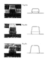
- Although CClF₃ has been used at relatively high pressures (less than 133 µbar) to etch polysilicon over silicon dioxide with excellent selectivity, the etching has not been anisotropic. Fig. 1 shows the etched profiles of N+ polysilicon etched at various pressures in pure CClF₃. Excessive undercutting can be seen at 133 µbar, as well as at much lower pressures. In pure CClF₃ at higher pressures there is thought to be an excess of Cl species over unsaturate species, CFx⁺. These chlorine species are low energy because of the high pressure and reduced mean free path. They diffuse in random directions and attack both vertical and horizontal surfaces of the layer being etched. Therefore, this p rocess produces substantial undercutting and has a poor directionality.
- A low pressure (33.25 µbar) RIE process has been developed for etching SiO₂ with respect to silicon. This involves the addition of molecular hydrogen to CClF₃. The addition of molecular hydrogen serves to getter the excess chlorine. This enhances the relative quantity of CFx⁺ in the ambient. At low pressures, CFx⁺ etches SiO₂ and because there is so little chlorine in the ambient, silicon does not etch.
- A process employing CCl₂F₂ and argon has been used to etch polysilicon overlying SiO₂ at moderate pressure. The selectivity of the process is low (7:1) and it is not anisotropic.
- A two-step process has been disclosed for etching layers of molybdenum silicide and polysilicon overlying SiO₂. Two different etch formulations are required for the two steps. The second etchant which is used to etch the polysilicon comprises CCl₂F₂ and C₂F₆.
- Pure CCl₂F₂ has also been used to etch polysilicon overlying SiO₂. However, the selectivity of the process is very low, especially at low power density where it approaches 2:1.
- It is an object of this invention to provide an improved process for the dry etching of silicon or silicides.
- It is a further object of this invention to provide a process for the dry etching of polysilicon or silicides which is both anisotropic and selective to an underlying layer of an oxide or nitride of silicon.
- It is another object of this invention to provide an anisotropic selective process for the dry etching of polysilicon or silicides which can be carried out at moderate to high pressures and low power density.
- Other objects will be apparent to those skilled in the art to which this invention pertains.
- In accordance with the invention, mixtures of CClF₃ and ammonia or of CCl₂F₂ and ammonia are employed at moderate pressures in a reactive ion etching chamber to anisotropically etch polysilicon or silicides with excellent selectivity to an underlying layer of an oxide or nitride of silicon.
- Figs. 1a, 1b and 1c are a series of SEMs showing the etched profiles of N+ polysilicon etched in pure CClF₃ at various pressures.
- Fig. 1a shows the profile obtained at 29.3 µbar.
- Fig. 1b shows the profile obtained at 79.8 µbar.
- Fig. 1c shows the profile obtained at 133 µbar.
- Fig. 2 is a schematic cross-sectional view of apparatus which can be used to carry out the process of the present invention.
- Fig. 3 is a schematic enlarged cross-sectional view of a substrate on which the process of this invention has been practiced.
- Figs. 4a, 4b, 4c and 4d are a series of SEMs showing the effect of the %NH₃ in CClF₃ on the etched profiles of N+ polysilicon at 133 µbar.
- Fig. 4a shows the effect of pure CClF₃.
- Fig. 4b shows the effect of 20% NH₃ in CClF₃ (v/v).
- Fig. 4c shows the effect of 30% NH₃ in CClF₃ (v/v).
- Fig. 4d shows the effect of 50% NH₃ in CClF₃ (v/v).
- Figs. 5a, 5b and 5c are a series of SEMs showing the effect of the %NH₃ in CClF₃ on the etched profiles of N+ polysilicon at 79.8 µbar.
- Fig. 5a shows the effect of pure CClF₃.
- Fig. 5b shows the effect of 20% NH₃ in CClF₃ (v/v).
- Fig. 5c shows the effect of 50% NH₃ in CClF₃ (v/v).
- Figs. 6a, 6b and 6c are SEMs showing the effect of the %NH₃ in CCl₂F₂ on the etched profiles on N+ polysilicon at 93.1 µbar.
- Fig. 6a shows pure CCl₂F₂.
- Fig. 6b shows 33.3% NH₃ by volume in CCl₂F₂.
- Fig. 6c shows 37.5% NH₃ by volume in CCl₂F₂.
- Elemental Silicon-containi ng layers: this refers to layers containing elemental silicon. These layers may be single crystal or polycrystalline. They may be doped to either conductivity type at any level. Silicon may be contained as part of an intermetallic compound such as a silicide of a refractory metal such as molybdenum, tungsten, titanium or tantalum.
- Covalent Silicon-containing compounds: this refers to chemical compounds containing silicon covalently bonded to other elements, such as nitrogen or oxygen. Such compounds include silicon oxide, silicon dioxide, silicon nitride, and silicon oxynitride.
- Plasma etching: etching which proceeds by means of a plasma generated by an RF discharge. The predominant removal mechanism is chemical reaction.
- Ion Beam Etching: etching which proceeds by means of accelerated species bombarding the surface to be etched. The predominant removal mechanism is physical momentum transfer. Also called ion milling or sputter etching.
- Reactive Ion Etching: etching which proceeds by means of a plasma in which the reactant species are accelerated toward the surface to be etched. The removal mechanism is a combination of chemical and physical interactions between the accelerated species and the surface.
- Etch Profile: wall configuration produced in an etched structure, which may be:
Vertical--straight walls on a plane with the resist edge and perpendicular to the surface of the substrate.
Undercut--sloped walls in which some portion of the wall lies under the resist. - Isotropic: etching which proceeds at a uniform rate in all directions (both vertically and laterally). It results in undercutting in which the etched region closest to the resist undercuts to a dimension approximately equal to that of the vertical etch dimension.
- Anisotropic: etching which is directional; that is, which proceeds faster in the vertical direction than in the lateral direction. Ideal anisotropic etching produces a vertical etch profile.
- Selectivity: the preferential etching of one substance over another which is a result of differences in the rate of chemical reaction between the etchant and each of the substances. It is expressed as the ratio of the etch rates of two adjacent layers (ERR).
- A typical reactive ion etching system is shown in Fig. 2. It comprises etching
chamber 10 containingparallel plate electrodes upper electrode 11 is grounded.Lower electrode 12 is powered byRF generator 13. Either or both electrodes may be water cooled and the distance between them may be adjustable. In a plasma etching system (not shown), the system configuration is similar, but the lower electrode is grounded and the upper electrode is powered. -
Etching chamber 10 is evacuated viaexhaust pipe 14 by pumping means (not shown). Etchant gas is supplied toetching chamber 10 throughgas inlet 16. The system may have multiple gas channels. The flow of the reactive gases can be controlled by pressure and/or flow-rate servo systems. - By introducing a suitable gas or gas mixture into
chamber 10 and establishing an electrical field betweenupper electrode 11 andlower electrode 12, a reactive plasma is generated. The plasma is characterized by a uniform dark space in the immediate vicinity ofcathode 12. Volatile products formed during the etching process are exhausted fromchamber 10 viaexhaust pipe 14. - The etchant gas mixture employed according to the present invention comprises:
- a. a gaseous fluorocarbon capable of supplying CFx and chlorine ions, and
- b. a gas capable of supplying hydrogen ions.
- Preferred gaseous fluorocarbons are CClF₃ and CCl₂F₂, and the preferred source of hydrogen ions is ammonia. The ammonia is employed in an amount effective to increase the selectivity, e.g. in a CClF₃: NH₃ ra tio or in a CCl₂F₂: NH₃ ratio (v/v) of about 80:20 to about 35:65.
- It is theorized that at 133 µbar with a pure gaseous fluorocarbon there is an excess of chlorine ions over unsaturate species, CFx. As noted above, this excess chlorine diffuses in random directions and attacks both vertical and horizontal surfaces producing substantial undercutting. The addition of hydrogen ions to the fluorocarbon removes the excess of chlorine ions and balances the concentration of CFx ions relative to chlorine ions. Ammonia is preferred over hydrogen gas as the source of hydrogen ions for two reasons. First, ammonia gas provides a much broader process window than hydrogen gas. This is important because if too much hydrogen is added, too much chlorine will be removed and unsaturate species, CFx, will predominate. The result of removing too much chlorine will depend on the pressure. At relatively high pressures, the unsaturate species, CFx, have low energy and coat out as a polymer on all exposed surfaces. The net result is a coating process instead of an etching process. At relatively low pressures, the unsaturate species, CFx, have high energy. As noted above, the addition of hydrogen to CClF₃ for example at low pressure (33.25 µbar) actually produces a process which can be viewed as the opposite of the present invention, i.e. the process will preferentially etch SiO₂ over Si, whereas the process of the present invention will preferentially etch Si over SiO₂. The CClF₃/H₂/low pressure process etches SIO₂ because of the predominance of high energy CFx species which are SiO₂ etchants. The second reason that ammonia is preferred over hydrogen gas as the source of hydrogen ions is because ammonia produces active nitrogen which is a polymer inhibitor. This gives the added benefit of a reduction in polymer formation. Of course, some polymer will still form on exposed surfaces. That which forms on horizontal surfaces will be removed by the chlorine species in a properly balanced mixture. That which forms on the sidewalls will not be attacked by the accelerated chlorine species and will further reduce the lateral etching which results in undercutting.
- It is sometimes desirable to employ an etchant gas mixture containing an inert gas. In this case, the ratio of the fluorocarbon to ammonia is kept the same as the composition without inerts. Inerts increase etch uniformity and help to cool the chamber. Examples of inerts which may be used are the noble gases, especially helium.
- The process of the present invention is used to etch articles with comprise a substrate (20) with one or more layers thereon. (See Fig. 3.) The method permits the preferential etching of an elemental silicon-containing layer (24) of doped polysilicon or a refractory metal silicide over a covalent silicon-containing layer (22) such as SiO, SiO₂, silicon nitride, or silicon oxynitride. When the process is used in the preparation of patterned articles, a mask (26) of, for instance, a photoresist or electron beam resist material is applied on top of the upper layer.
- The process of the present invention is preferably carried out under vacuum at pressures between about 79.8 and 133 µbar. Pressures higher than 133 µbar ordinarily are not employed because they cause an excessive amount of polymer to coat out on the surfaces, as will be discussed hereinafter. Pressures lower than about 79.8 µbar result in a reduction in selectivity.
- The total flow rate of the gases is generally 15 to 100 SCCM, preferably about 30 to 60 (standard conditions of 25°C and 1.011 bar).
- The RF power supply was operated at a power density between about 0.125 and 0.3 or 0.2 and 0.3 watts/cm². However, these parameters will be dependent on the apparatus employed.
- General conditions: a parallel plate, radial flow reactor was used. The space bet ween the anode and the cathode was about 9-10 cm. All parts within the etch chamber are constructed of aluminum. RF power at 13.56 MH z is capacitatively coupled to the bottom electrode while the top electrode and chamber wall are well grounded. The power density is 0.22 W/cm². The etch gases are introduced through a manifold arrangement at the front of the chamber and evacuated at the back. Etch rates are measured from a laser interferometer trace or by measuring film thickness before and after etch on an IBM 3820 Film Thickness Analyzer. Selectivities are calculated from the measured etch rates.
- The substrates are single crystal silicon wafers with <100> orientation. To obtain the MOS structure, 25 nm of gate thermal oxide was grown. Then polysilicon was deposited using LPCVD at 625° C. The polysilicon was subsequently doped with POCl₃. The substrates in examples 1, 2 and 3 had 430 nm of polysilicon. The substrates in examples 4 and 5 had 170 nm of polysilicon on which 250 nm of tungsten silicide was deposited using co-evaporation.
- Pressure -- 79.8 µbar
Flow rate -- 40 sccm
%NH3 -- 20% - An etch rate of 49 nm/minute was realized in N+ polysilicon. The etch profile was vertical and the ERR of polysilicon to SiO₂ was 11:1.
- Pressure -- l06.4 µbar
Flow rate -- 40 sccm
%NH3 -- 35% - An etch rate of 54 nm/minute was realized in N+ polysilicon. The etch profile was vertical and the ERR of polysilicon to SiO₂ was l8:1.
- Pressure -- 133 µbar
Flow rate -- 40 sccm
%NH3 -- 45% - An etch rate of 62 nm/minute was realized in N+ polysilicon. The etch profile was vertical and the ERR of polysilicon to SiO₂ was 31:1.
- Pressure -- 106.4 µbar
Flow rate -- 40 sccm
%NH3 -- 35% - An etch rate of 54 nm/minute was realized in tungsten silicide. The etch profile was vertical and the ERR of silicide to SiO₂ was 18:1.
- Pressure -- 133 µbar
Flow rate -- 40 sccm
%NH3 -- 45% - An etch rate of 62 nm/minute was realized in tungsten silicide. The etch profile was vertical and the ERR of silicide to SiO₂ was 31:1.
- While the invention has been described in conjunction with a reactive ion etching apparatus, it will be understood that a variety of reactors may be employed satisfactorily. Different etching modes, including chemically based concepts like plasma etching and physically based concepts like reactive ion beam etching should be possible with the plasma environments disclosed. It is to be understood that the above-described arrangements and procedures are only illustrative of the principles of the present invention. Various alterations in form and detail may be made without departing from the spirit and scope of the invention.
Claims (18)
Applications Claiming Priority (4)
| Application Number | Priority Date | Filing Date | Title |
|---|---|---|---|
| US76983285A | 1985-08-27 | 1985-08-27 | |
| US76964785A | 1985-08-27 | 1985-08-27 | |
| US769832 | 1985-08-27 | ||
| US769647 | 1985-08-27 |
Publications (3)
| Publication Number | Publication Date |
|---|---|
| EP0212585A2 true EP0212585A2 (en) | 1987-03-04 |
| EP0212585A3 EP0212585A3 (en) | 1988-04-27 |
| EP0212585B1 EP0212585B1 (en) | 1991-12-18 |
Family
ID=27118205
Family Applications (1)
| Application Number | Title | Priority Date | Filing Date |
|---|---|---|---|
| EP19860111282 Expired - Fee Related EP0212585B1 (en) | 1985-08-27 | 1986-08-14 | Selective and anisotropic dry etching |
Country Status (2)
| Country | Link |
|---|---|
| EP (1) | EP0212585B1 (en) |
| DE (1) | DE3682976D1 (en) |
Cited By (2)
| Publication number | Priority date | Publication date | Assignee | Title |
|---|---|---|---|---|
| EP0553961A2 (en) * | 1992-01-29 | 1993-08-04 | Applied Materials, Inc. | Reactive ion etch process including hydrogen radicals |
| FR2765393A1 (en) * | 1997-06-25 | 1998-12-31 | France Telecom | Plasma etching of polycrystalline silicon@-germanium@ layer |
Citations (2)
| Publication number | Priority date | Publication date | Assignee | Title |
|---|---|---|---|---|
| FR2230148A1 (en) * | 1973-05-17 | 1974-12-13 | Itt | |
| DE3118839A1 (en) * | 1980-05-14 | 1982-02-18 | Hitachi, Ltd., Tokyo | DRY WET PROCESS |
-
1986
- 1986-08-14 DE DE8686111282T patent/DE3682976D1/en not_active Expired - Fee Related
- 1986-08-14 EP EP19860111282 patent/EP0212585B1/en not_active Expired - Fee Related
Patent Citations (2)
| Publication number | Priority date | Publication date | Assignee | Title |
|---|---|---|---|---|
| FR2230148A1 (en) * | 1973-05-17 | 1974-12-13 | Itt | |
| DE3118839A1 (en) * | 1980-05-14 | 1982-02-18 | Hitachi, Ltd., Tokyo | DRY WET PROCESS |
Non-Patent Citations (1)
| Title |
|---|
| JOURNAL OF VACUUM SCIENCE & TECHNOLOGY: PART B, vol. 3, no. 1, second series, January-February 1985, pages 16-19, American Vacuum Society, new York, US; M. KIMIZUKA et al.: "Pattern profile control of polysilicon plasma etching" * |
Cited By (5)
| Publication number | Priority date | Publication date | Assignee | Title |
|---|---|---|---|---|
| EP0553961A2 (en) * | 1992-01-29 | 1993-08-04 | Applied Materials, Inc. | Reactive ion etch process including hydrogen radicals |
| EP0553961A3 (en) * | 1992-01-29 | 1995-09-27 | Applied Materials Inc | Reactive ion etch process including hydrogen radicals |
| FR2765393A1 (en) * | 1997-06-25 | 1998-12-31 | France Telecom | Plasma etching of polycrystalline silicon@-germanium@ layer |
| EP0905759A1 (en) * | 1997-06-25 | 1999-03-31 | France Telecom | Process for etching a polycristalline Si1-xGex layer or stacked layers of polycristalline Si1-xGex and Si, and application to electronic devices |
| US6271144B1 (en) | 1997-06-25 | 2001-08-07 | France Telecom | Process for etching a polycrystalline Si(1-x)Ge(x) layer or a stack of polycrystalline Si(1-x)Ge(x) layer and of a polycrystalline Si layer, and its application to microelectronics |
Also Published As
| Publication number | Publication date |
|---|---|
| EP0212585B1 (en) | 1991-12-18 |
| EP0212585A3 (en) | 1988-04-27 |
| DE3682976D1 (en) | 1992-01-30 |
Similar Documents
| Publication | Publication Date | Title |
|---|---|---|
| US4734157A (en) | Selective and anisotropic dry etching | |
| US5286344A (en) | Process for selectively etching a layer of silicon dioxide on an underlying stop layer of silicon nitride | |
| US7049244B2 (en) | Method for enhancing silicon dioxide to silicon nitride selectivity | |
| US4713141A (en) | Anisotropic plasma etching of tungsten | |
| JP4579611B2 (en) | Dry etching method | |
| EP0482519B1 (en) | Method of etching oxide materials | |
| US5814563A (en) | Method for etching dielectric using fluorohydrocarbon gas, NH3 -generating gas, and carbon-oxygen gas | |
| US5256245A (en) | Use of a clean up step to form more vertical profiles of polycrystalline silicon sidewalls during the manufacture of a semiconductor device | |
| US5180464A (en) | Dry etching method | |
| US4465552A (en) | Method of selectively etching silicon dioxide with SF6 /nitriding component gas | |
| US5024722A (en) | Process for fabricating conductors used for integrated circuit connections and the like | |
| US20050037624A1 (en) | Method for plasma etching performance enhancement | |
| US5453156A (en) | Anisotropic polysilicon plasma etch using fluorine gases | |
| US5880033A (en) | Method for etching metal silicide with high selectivity to polysilicon | |
| US4836886A (en) | Binary chlorofluorocarbon chemistry for plasma etching | |
| US4373990A (en) | Dry etching aluminum | |
| US6756314B2 (en) | Method for etching a hard mask layer and a metal layer | |
| US5536364A (en) | Process of plasma etching silicon | |
| US4364793A (en) | Method of etching silicon and polysilicon substrates | |
| US6069087A (en) | Highly selective dry etching process | |
| KR20010109187A (en) | Method of anisotropic plasma etching using non-chlorofluorocarbon, fluorine-based chemistry | |
| EP0212585B1 (en) | Selective and anisotropic dry etching | |
| Ephrath | The effect of cathode materials on reactive ion etching of silicon and silicon dioxide in a CF 4 plasma | |
| US6228774B1 (en) | High aspect ratio sub-micron contact etch process in an inductively-coupled plasma processing system | |
| Smolinsky et al. | Reactive ion etching of silicon oxides with ammonia and trifluoromethane. The role of nitrogen in the discharge |
Legal Events
| Date | Code | Title | Description |
|---|---|---|---|
| PUAI | Public reference made under article 153(3) epc to a published international application that has entered the european phase |
Free format text: ORIGINAL CODE: 0009012 |
|
| AK | Designated contracting states |
Kind code of ref document: A2 Designated state(s): DE FR GB |
|
| 17P | Request for examination filed |
Effective date: 19870623 |
|
| PUAL | Search report despatched |
Free format text: ORIGINAL CODE: 0009013 |
|
| RHK1 | Main classification (correction) |
Ipc: H01L 21/31 |
|
| AK | Designated contracting states |
Kind code of ref document: A3 Designated state(s): DE FR GB |
|
| 17Q | First examination report despatched |
Effective date: 19900622 |
|
| GRAA | (expected) grant |
Free format text: ORIGINAL CODE: 0009210 |
|
| AK | Designated contracting states |
Kind code of ref document: B1 Designated state(s): DE FR GB |
|
| ET | Fr: translation filed | ||
| REF | Corresponds to: |
Ref document number: 3682976 Country of ref document: DE Date of ref document: 19920130 |
|
| PLBE | No opposition filed within time limit |
Free format text: ORIGINAL CODE: 0009261 |
|
| STAA | Information on the status of an ep patent application or granted ep patent |
Free format text: STATUS: NO OPPOSITION FILED WITHIN TIME LIMIT |
|
| 26N | No opposition filed | ||
| PGFP | Annual fee paid to national office [announced via postgrant information from national office to epo] |
Ref country code: GB Payment date: 19960724 Year of fee payment: 11 |
|
| PGFP | Annual fee paid to national office [announced via postgrant information from national office to epo] |
Ref country code: FR Payment date: 19960806 Year of fee payment: 11 |
|
| PGFP | Annual fee paid to national office [announced via postgrant information from national office to epo] |
Ref country code: DE Payment date: 19960828 Year of fee payment: 11 |
|
| PG25 | Lapsed in a contracting state [announced via postgrant information from national office to epo] |
Ref country code: GB Free format text: LAPSE BECAUSE OF NON-PAYMENT OF DUE FEES Effective date: 19970814 |
|
| GBPC | Gb: european patent ceased through non-payment of renewal fee |
Effective date: 19970814 |
|
| PG25 | Lapsed in a contracting state [announced via postgrant information from national office to epo] |
Ref country code: FR Free format text: LAPSE BECAUSE OF NON-PAYMENT OF DUE FEES Effective date: 19980430 |
|
| PG25 | Lapsed in a contracting state [announced via postgrant information from national office to epo] |
Ref country code: DE Free format text: LAPSE BECAUSE OF NON-PAYMENT OF DUE FEES Effective date: 19980501 |
|
| REG | Reference to a national code |
Ref country code: FR Ref legal event code: ST |