EP0209630B1 - Heat transfer element and its use in a circuit package - Google Patents
Heat transfer element and its use in a circuit package Download PDFInfo
- Publication number
- EP0209630B1 EP0209630B1 EP86102647A EP86102647A EP0209630B1 EP 0209630 B1 EP0209630 B1 EP 0209630B1 EP 86102647 A EP86102647 A EP 86102647A EP 86102647 A EP86102647 A EP 86102647A EP 0209630 B1 EP0209630 B1 EP 0209630B1
- Authority
- EP
- European Patent Office
- Prior art keywords
- fins
- foil
- heat transfer
- cavity
- foils
- Prior art date
- Legal status (The legal status is an assumption and is not a legal conclusion. Google has not performed a legal analysis and makes no representation as to the accuracy of the status listed.)
- Expired - Lifetime
Links
Images


Classifications
-
- F—MECHANICAL ENGINEERING; LIGHTING; HEATING; WEAPONS; BLASTING
- F28—HEAT EXCHANGE IN GENERAL
- F28F—DETAILS OF HEAT-EXCHANGE AND HEAT-TRANSFER APPARATUS, OF GENERAL APPLICATION
- F28F13/00—Arrangements for modifying heat-transfer, e.g. increasing, decreasing
- F28F13/18—Arrangements for modifying heat-transfer, e.g. increasing, decreasing by applying coatings, e.g. radiation-absorbing, radiation-reflecting; by surface treatment, e.g. polishing
- F28F13/185—Heat-exchange surfaces provided with microstructures or with porous coatings
- F28F13/187—Heat-exchange surfaces provided with microstructures or with porous coatings especially adapted for evaporator surfaces or condenser surfaces, e.g. with nucleation sites
-
- F—MECHANICAL ENGINEERING; LIGHTING; HEATING; WEAPONS; BLASTING
- F28—HEAT EXCHANGE IN GENERAL
- F28F—DETAILS OF HEAT-EXCHANGE AND HEAT-TRANSFER APPARATUS, OF GENERAL APPLICATION
- F28F3/00—Plate-like or laminated elements; Assemblies of plate-like or laminated elements
- F28F3/02—Elements or assemblies thereof with means for increasing heat-transfer area, e.g. with fins, with recesses, with corrugations
-
- H—ELECTRICITY
- H10—SEMICONDUCTOR DEVICES; ELECTRIC SOLID-STATE DEVICES NOT OTHERWISE PROVIDED FOR
- H10W—GENERIC PACKAGES, INTERCONNECTIONS, CONNECTORS OR OTHER CONSTRUCTIONAL DETAILS OF DEVICES COVERED BY CLASS H10
- H10W40/00—Arrangements for thermal protection or thermal control
- H10W40/70—Fillings or auxiliary members in containers or in encapsulations for thermal protection or control
- H10W40/73—Fillings or auxiliary members in containers or in encapsulations for thermal protection or control for cooling by change of state
-
- H—ELECTRICITY
- H10—SEMICONDUCTOR DEVICES; ELECTRIC SOLID-STATE DEVICES NOT OTHERWISE PROVIDED FOR
- H10W—GENERIC PACKAGES, INTERCONNECTIONS, CONNECTORS OR OTHER CONSTRUCTIONAL DETAILS OF DEVICES COVERED BY CLASS H10
- H10W72/00—Interconnections or connectors in packages
- H10W72/071—Connecting or disconnecting
- H10W72/072—Connecting or disconnecting of bump connectors
- H10W72/07251—Connecting or disconnecting of bump connectors characterised by changes in properties of the bump connectors during connecting
-
- H—ELECTRICITY
- H10—SEMICONDUCTOR DEVICES; ELECTRIC SOLID-STATE DEVICES NOT OTHERWISE PROVIDED FOR
- H10W—GENERIC PACKAGES, INTERCONNECTIONS, CONNECTORS OR OTHER CONSTRUCTIONAL DETAILS OF DEVICES COVERED BY CLASS H10
- H10W72/00—Interconnections or connectors in packages
- H10W72/20—Bump connectors, e.g. solder bumps or copper pillars; Dummy bumps; Thermal bumps
Definitions
- This invention relates to a heat transfer element with nucleate boiling and to its use in a package for electronic circuits.
- a semiconductor chip is mounted on a dielectric chip carrier that contains part of the circuit wiring, and the chip carrier with the chips is assembled with an enclosure or cover that holds a dielectric liquid. Heat is transferred from the chips to the liquid and then from the dielectric liquid to the atmosphere or to a water supply. In some circuit packages heat is transferred from the chip to the dielectric liquid by a mechanism called nucleate boiling.
- Nucleate boiling is described in detail in U. S. patent 4,050,507 of Richard C. Chu and Kevin P. Moran and their explanation will be repeated here only to a limited extent to establish the terminology.
- heat from a heat generating subject goes to break the inter-molecular bonds of the liquid and to overcome the pressure of nearby molecules.
- "Nucleate” means that vapor bubbles form and grow from nucleation sites. The nucleation sites commonly trap bubbles of gas or vapor and these bubbles reduce the temperature required for nucleation.
- the nucleation sites are formed by cavities in the surface of the heat generating subject.
- Fig. 1 of the Chu and Moran patent is a plot showing different modes of heat transfer that take place at different values of heat flux and temperature excess. (Temperature excess is the difference between the temperature of the heat generating component and the saturation temperature of the dielectric liquid.) The plot illustrates that nucleate boiling handles large increases in heat flux with only small increases in temperature. At a lower temperature, the heat transfer occurs by convection, and at a higher temperature heat transfer occurs by a mechanism called film boiling.
- Fig. 12 of the patent shows a cross section of a desirable nucleate boiling cavity, and it will be used to illustrate part of the terminology for this specification. It will be convenient to assign names to the inner walls of the cavity as though the walls of the cavity were built up from separate components even though the demarcation may be faint in an actual device: in the preferred heat transfer elements these names will correspond to particular steps in the method of manufacture.
- the heat transfer element is arbitrarily oriented with its nucleate boiling surface horizontal and facing upward in contact with a boiling liquid.
- the cavity has a top at the plane of the nucleate boiling surface (or in Fig. 12 the top is rimmed slightly above the surface).
- the cavity has a bottom remote from this surface.
- the cavity is jug shaped with a narrow entrance or mouth and a wider main cavity below the entrance.
- the sides of the main cavity are approximately cylindrical as a result of the method of forming the cavity, and the main cavity has an approximate predetermined diameter.
- the surface of the cavity that in Fig. 12 flares outward from the entrance to approximately the predetermined diameter will be called the ceiling, and in Fig. 12 this surface is concave.
- the approximately horizontal surface at the bottom of the cavity will be called the floor.
- the heat transfer element can of course be oriented with its nucleate boiling surface in any direction and the same terminology can be used.
- Figs. 2 and 3 of the patent show the growth of a vapor bubble in a nucleate boiling site. Bubbles of gas exist in the cavities because the dielectric liquid contains dissolved gas and because vapor bubbles are formed during the normal operation of the device. The patent also explains that supplemental vapor bubbles can be injected into the dielectric liquid. However, the vapor or gas bubble can be lost from the cavities and this loss causes the nucleate boiling surface to become less effective. Loss of the bubble can be understood best from the viewpoint that the dielectric liquid floods the cavity. Flooding of a nucleate boiling surface with cavities is therefore highly undesirable.
- the liquid floods the cavity because it wets the cavity surfaces that were otherwise in contact with a gas or vapor bubble.
- Fig. 4 of the patent illustrates the general effect of the surface tension
- Figs. 5 and 6 show how the dielectric liquid can flood the cavity.
- the wettability of a liquid is expressed numerically as the contact angle that is formed between a drop of the liquid and a flat substrate. For example, a highly wetting liquid would spread over the substrate into a film and the angle between the surface of the substrate and the surface of the film would approach 180 degrees. A non- wetting liquid would tend to form a sphere touching the substrate at only a point with a contact angle approaching 0 degrees. Typical dielectric liquids have low contact angles and thus more easily flood the cavities. In the cavity of Fig. 12, the narrow cavity entrance reduces flooding.
- the prior art teaches first making small holes in a thin metal foil and then folding the foil over to form two layers. Except where the holes match up in the two foil parts, each hole is backed by the solid surface of the other foil. Thus, the two foil parts have many small outwardly facing cavities.
- the invention is particularly intended for cooling electronic components but it will be useful in other applications.
- the heat transfer element of the invention is formed by laminating two thin metal foils that each have holes formed in a new way.
- two part through holes are formed with a larger diameter part opening to the inner surface and forming a main cavity in the heat transfer element and a smaller diameter hole part opening to the outer surface and forming the entrance of the nucleate boiling cavity in the heat transfer element.
- the sides of the hole steps are generally cylindrical as in the Chu and Moran Fig. 12.
- the top of the first step forms the ceiling of the cavity and it has a convex shape that produces an angle of greater than 90 degrees in the path of the liquid entering the cavity.
- the first and second step holes are formed in one punch operation or are formed separately.
- the fins can also be made of two foils of different metals with differing coefficients of thermal expansion so that the bimetal effect causes the fins to bend as they heat. This effect is controlled to cause the fins to fan open when the temperature increases and to thereby allow better circulation of the boiling liquid. When the fin temperature decreases the fins bend closer together and reduce the circulation of the coolant and thereby prevent overcooling the associated component.
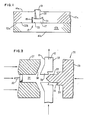
- Fig. 1 shows a section of a foil 12a having a surface 14a that faces a boiling liquid (not shown).
- the nucleate boiling cavity 15 has a main cavity 17 with a generally cylindrical side wall 18 and an entrance 19 with a generally cylindrical side wall 20. Between side walls 18 and 20 the cavity is bounded by a convex ceiling 21.
- Foil surface 22a is designated the inside surface and it faces the inside surface 22b of a second foil 12b.
- Surface 22b forms the floor 23 of cavity 15.
- foil 12b has similar nucleate boiling cavities opening to its outer surface 14b.
- element 12b in Fig. 1 represents any heat transfer element to which foil 12a might be attached to provide a nucleate boiling surface or any suitable structure to provide floor 23 for cavity 15.
- the main cavity 17 is formed in a first step and the entrance 19 is formed in a second step and in another embodiment the main cavity and entrance are formed in a single step.
- Fig. 2 illustrates the method using two steps and
- Fig. 3 illustrates the method using one step. Both Figs. 2 and 3 illustrate features that are useful in either method. It will be convenient to describe the physical structure of the nucleate boiling cavity as though the cavity 17 and entrance 19 were distinct entities formed in separate steps.
- Fig. 2E is an edge view of two laminated foils 12a, 12b and will be familiar from the description of Fig. 1.
- Figs. 2A - 2D show manufacturing steps that in- dude folding a single foil to form the two layer structure of Fig. 2E.
- Reference characters 12, 14 and 22 (without subscripts) identify the unfolded foil and its outer and inner surfaces respectively to correspond to the terminology of the individual foils.
- a dashed line extends through the edge views of the foil and identifies a point of folding the foil to form the distinct foils 12a and 12b of Fig. 1. In Fig. 2E the dashed line coincides with the meeting surface of the two inside surfaces 22a, 22b.
- the unfolded foil 12 in Fig. 2A is a sheet of copper or aluminum or other metal or metal alloy that has good heat conductivity.
- the preferred foil is also easily punched and easily bent into the final folded fin form.
- the foil thickness is about 0.1 to 0.2 mm.
- Fig. 2B shows foil 12 after an operation of punching from the inside surface 22 to form holes that will be the main cavities 17 in the finished product of Fig. 2E. Only a few holes are shown in the drawing.
- the holes have substantially cylindrical side walls 18 and they have a convex ceiling 21 as introduced in the description of Fig. 1.
- the punching operation domes the foil outwardly at points 33 above the holes with material displaced from hole 17. The punching operation will be described more specifically in the description of Fig. 3.
- Fig. 2C shows the foil after the step of forming the second hole 19 between the outside surface 14 of the foil and the ceiling 21 of the main cavity 17.
- Hole 19 is formed by any suitable technique that preserves or enhances the convex shape of the cavity ceiling 21, preferably by punching or mechanical drilling or by laser drilling. Note that the structure of Fig. 2C is achieved whether the holes are formed in two steps as in Fig. 2B and 2C or in one step as will be described later.
- Figs. 2D shows the step of folding the foil
- Fig. 2E shows the completed fin structure with the inside surfaces 22a and 22b in contact.
- Fig. 3 shows the foil 12 of Fig. 1 with a punch 26 facing the foil inside surface 22 and a die 27 facing the foil outside surface 14.
- Suitable punching techniques are well known, and the components of the punch are shown diagrammatically.
- the punch and die are positioned in the drawing to show their relationship to the surfaces of the hole formed in the foil but the positions correspond to retracting the die and the punch after a punching operation.
- Punch 26 has a base 29, and it has surfaces 31, 32 and 33 that form respectively the sidewall 18 and ceiling 22 of the main cavity and the sidewall entrance 19.
- Die 27 has a hole 34 that receives the material (not shown) that is removed from the entrance of the cavity and an ejector 35 drives the material out of the hole at the end of the punching operation.
- the die has a conical depression 36 that permits the foil to be displaced in a conical rim 38 as material is moved out of the region of the main cavity.
- the punch for the method of Fig. 2 is a simplification of the punch shown in Fig. 3, without part 33 that forms the surface 18 of entrance 19 and with the surface 32 formed as a concave cone corresponding to the unfinished ceiling 21 in Fig. 2B.
- Fig. 4 is similar in part to Fig. 2E but additionally shows the foils 12a, 12b bent in a sinuous shape to form a series of fins that are spaced apart by an intervening single layer of the foil forming a base 41 for attachment to a heat generating subject such as a silicon chip (not shown) or, equivalently, to an intermediate heat transferring subject 42.
- a heat generating subject such as a silicon chip (not shown) or, equivalently, to an intermediate heat transferring subject 42.
- a molybdenum pad 42 is attached to the pad by means such as solder 45.
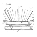
- FIG. 5A and 5B show the molybdenum pad 42, and solder 45 of Fig. 4 and additionally show a conventional chip 48, chip carrier 49 and solder balls 50 that electrically and mechanically interconnect conductive pads on the chip and pads on the chip carrier. (The thin pads are not shown in the drawing.)
- a barrier 52 separates chip 48 from the dielectric liquid.
- the barrier can be made of a flexible metal or polymer material.
- Fig. 5A shows the fins extending co-parallel and perpendicular to the back of the chip
- Fig. 5B shows the fins spread apart.
- the dielectric liquid 51 is circulated through the fins, either by a pump or by temperature differences, and the fanned out fins of Fig. 5B permit increased circulation and increased cooling.
- the folded fin structure of Figs. 2E and 4 can be fixed in any suitable spacing to provide a selected amount of cooling. In a circuit package with several chips that operate at different power, and thereby have different cooling requirements, the fins of higher powered chips can be set wider apart and the fins of lower powered chips can be set closer together to provide sufficient cooling for the higher powered chips without over cooling the lower powered chips.
- Figs. 5A and 5B also show a bimetal fin structure that provides a self adjusting heat transfer element.
- the two foils are not folded from a single sheet but are of separate materials that have different coefficients of thermal expansion.
- Suitable metals are a soft copper and molybdenum, and the foils are designated 12c and 12m for the higher coefficient material and the lower coefficient material respectively.
- the layers 12c and 12m are suitably laminated, for example by soldering or by an adhesive.
- An increase in temperature causes the bimetal structure to bend in the direction of the foil 12m having the lower coefficient of expansion, and the foils are arranged symmetrically about the mid line 62 of the chip so that the fins fan out as shown in Fig. 5B.
- Fig. 5B shows, adjacent fins or adjacent sets of fins are made to bend differently so that the outside fins bend more than the fins toward the mid line 62. (If the fins were identical, the fins would bend through equal angles and would actually be slightly closer together in the spread condition of Fig. 5B.)
- the fins are made of progressively different materials for one or both of layers 12c and 12m.
- the ratio of the thickness of the layers 12c and 12m is varied: the high coefficient layer 12c is made thicker for fins near the mid line or, conversely, the low coefficient layer 12m is made thinner for fins near the outside.
- the base 41 can be attached to the inside of a pipe that carries a liquid to be boiled or to the outside of a pipe that is submerged in a liquid to be boiled.
Landscapes
- Engineering & Computer Science (AREA)
- Physics & Mathematics (AREA)
- Thermal Sciences (AREA)
- Mechanical Engineering (AREA)
- General Engineering & Computer Science (AREA)
- Chemical & Material Sciences (AREA)
- Crystallography & Structural Chemistry (AREA)
- Cooling Or The Like Of Semiconductors Or Solid State Devices (AREA)
Description
- This invention relates to a heat transfer element with nucleate boiling and to its use in a package for electronic circuits.
- This invention is useful broadly in heat transfer apparatus, but it will be helpful to consider a specific circuit package that would use the invention. A semiconductor chip is mounted on a dielectric chip carrier that contains part of the circuit wiring, and the chip carrier with the chips is assembled with an enclosure or cover that holds a dielectric liquid. Heat is transferred from the chips to the liquid and then from the dielectric liquid to the atmosphere or to a water supply. In some circuit packages heat is transferred from the chip to the dielectric liquid by a mechanism called nucleate boiling.
- Nucleate boiling is described in detail in U. S. patent 4,050,507 of Richard C. Chu and Kevin P. Moran and their explanation will be repeated here only to a limited extent to establish the terminology. When a dielectric liquid is converted to a vapor by boiling, heat from a heat generating subject goes to break the inter-molecular bonds of the liquid and to overcome the pressure of nearby molecules. "Nucleate" means that vapor bubbles form and grow from nucleation sites. The nucleation sites commonly trap bubbles of gas or vapor and these bubbles reduce the temperature required for nucleation. In the apparatus of this invention and in the apparatus of Chu and Moran the nucleation sites are formed by cavities in the surface of the heat generating subject.
- Fig. 1 of the Chu and Moran patent is a plot showing different modes of heat transfer that take place at different values of heat flux and temperature excess. (Temperature excess is the difference between the temperature of the heat generating component and the saturation temperature of the dielectric liquid.) The plot illustrates that nucleate boiling handles large increases in heat flux with only small increases in temperature. At a lower temperature, the heat transfer occurs by convection, and at a higher temperature heat transfer occurs by a mechanism called film boiling.
- Fig. 12 of the patent shows a cross section of a desirable nucleate boiling cavity, and it will be used to illustrate part of the terminology for this specification. It will be convenient to assign names to the inner walls of the cavity as though the walls of the cavity were built up from separate components even though the demarcation may be faint in an actual device: in the preferred heat transfer elements these names will correspond to particular steps in the method of manufacture. To establish the terminology, the heat transfer element is arbitrarily oriented with its nucleate boiling surface horizontal and facing upward in contact with a boiling liquid. The cavity has a top at the plane of the nucleate boiling surface (or in Fig. 12 the top is rimmed slightly above the surface). The cavity has a bottom remote from this surface. The cavity is jug shaped with a narrow entrance or mouth and a wider main cavity below the entrance. The sides of the main cavity are approximately cylindrical as a result of the method of forming the cavity, and the main cavity has an approximate predetermined diameter. The surface of the cavity that in Fig. 12 flares outward from the entrance to approximately the predetermined diameter will be called the ceiling, and in Fig. 12 this surface is concave. The approximately horizontal surface at the bottom of the cavity will be called the floor. The heat transfer element can of course be oriented with its nucleate boiling surface in any direction and the same terminology can be used.
- Figs. 2 and 3 of the patent show the growth of a vapor bubble in a nucleate boiling site. Bubbles of gas exist in the cavities because the dielectric liquid contains dissolved gas and because vapor bubbles are formed during the normal operation of the device. The patent also explains that supplemental vapor bubbles can be injected into the dielectric liquid. However, the vapor or gas bubble can be lost from the cavities and this loss causes the nucleate boiling surface to become less effective. Loss of the bubble can be understood best from the viewpoint that the dielectric liquid floods the cavity. Flooding of a nucleate boiling surface with cavities is therefore highly undesirable.
- Whether the liquid will flood the cavities depends partly on the surface tension or wettability of the liquid: the liquid floods the cavity because it wets the cavity surfaces that were otherwise in contact with a gas or vapor bubble. Fig. 4 of the patent illustrates the general effect of the surface tension, and Figs. 5 and 6 show how the dielectric liquid can flood the cavity. The wettability of a liquid is expressed numerically as the contact angle that is formed between a drop of the liquid and a flat substrate. For example, a highly wetting liquid would spread over the substrate into a film and the angle between the surface of the substrate and the surface of the film would approach 180 degrees. A non- wetting liquid would tend to form a sphere touching the substrate at only a point with a contact angle approaching 0 degrees. Typical dielectric liquids have low contact angles and thus more easily flood the cavities. In the cavity of Fig. 12, the narrow cavity entrance reduces flooding.
- Flooding can also be inhibited if the liquid is made to flow over angles in the surface as it spreads into a cavity. In the analysis to calculate whether the liquid will flood the cavity, an angle in this path is combined with the contact angle. It is known that the cavity shape of Fig. 12 would be improved if the surface between the entrance and the side walls were concave, flaring outwardly and upwardly from the entrance to the side walls, instead of outwardly and downwardly. This shape produces an angle of more than 270 degrees in the path that the liquid must take to flood the cavity. A cavity with this shape can be said to have an approximate cardoid shape.
- The prior art teaches first making small holes in a thin metal foil and then folding the foil over to form two layers. Except where the holes match up in the two foil parts, each hole is backed by the solid surface of the other foil. Thus, the two foil parts have many small outwardly facing cavities.
- It is therefore the object of the present invention to provide an improved heat transfer element of the aforementioned kind that contains cavities which cannot be flooded and that is convenient to manufacture; in addition an improved circuit package for electronic circuits shall be provided that makes use of such heat transfer elements.
- This object is achieved by the invention as described in
claims 1 and 6; embodiments of the invention are characterized in the dependent claims. - The invention is particularly intended for cooling electronic components but it will be useful in other applications.
- The heat transfer element of the invention is formed by laminating two thin metal foils that each have holes formed in a new way. In preparing the foils before the lamination step, two part through holes are formed with a larger diameter part opening to the inner surface and forming a main cavity in the heat transfer element and a smaller diameter hole part opening to the outer surface and forming the entrance of the nucleate boiling cavity in the heat transfer element. The sides of the hole steps are generally cylindrical as in the Chu and Moran Fig. 12. The top of the first step forms the ceiling of the cavity and it has a convex shape that produces an angle of greater than 90 degrees in the path of the liquid entering the cavity. When two foils are laminated inside to inside, the inner surface of each foil forms the floor of the cavities of the other foil. The first and second step holes are formed in one punch operation or are formed separately.
- If the ribbon of the foil is folded inside to inside in a rosette fashion a series of closely spaced fins that extend from a base is obtained. This structure provides easy expansion in a direction at right angles to the lines of fins.
- The fins can also be made of two foils of different metals with differing coefficients of thermal expansion so that the bimetal effect causes the fins to bend as they heat. This effect is controlled to cause the fins to fan open when the temperature increases and to thereby allow better circulation of the boiling liquid. When the fin temperature decreases the fins bend closer together and reduce the circulation of the coolant and thereby prevent overcooling the associated component.
- Preferred embodiments of the invention will now be described with reference to the drawings.
-
- Fig. 1 is a section view of two laminated foils showing a nucleate boiling cavity according to this invention.
- Figs. 2A through 2E show a section view of a foil in a sequence of steps for forming the nucleate boiling cavities and folding the foil into the laminated heat transfer structure of Fig. 1.
- Fig. 3 shows a punch and die and a section of a foil where a hole has been punched that will become a nucleate boiling cavity in the completed heat transfer structure.
- Fig. 4 is a section view of a fin structure using the nucleate boiling foil.
- Figs. 5A and 5B are section views of a circuit package using fins having the nucleate boiling surface of Fig. 1. Fig. 5A shows the fins closely spaced to reduce the coolant flow and Fig. 5B shows the fins spread apart for enhanced coolant flow. Figs. 5A and 5B also illustrate a bimetal fin structure that automatically adjusts the fin spacing for temperature control.
- The general shape of the nucleate boiling cavity has been introduced earlier in this specification. Fig. 1 shows a section of a
foil 12a having asurface 14a that faces a boiling liquid (not shown). The nucleate boilingcavity 15 has amain cavity 17 with a generallycylindrical side wall 18 and anentrance 19 with a generallycylindrical side wall 20. Betweenside walls convex ceiling 21.Foil surface 22a is designated the inside surface and it faces theinside surface 22b of asecond foil 12b.Surface 22b forms thefloor 23 ofcavity 15. - For most applications of this invention,
foil 12b has similar nucleate boiling cavities opening to its outer surface 14b. From an alternative viewpoint,element 12b in Fig. 1 represents any heat transfer element to whichfoil 12a might be attached to provide a nucleate boiling surface or any suitable structure to providefloor 23 forcavity 15. - In one embodiment of our method the
main cavity 17 is formed in a first step and theentrance 19 is formed in a second step and in another embodiment the main cavity and entrance are formed in a single step. Fig. 2 illustrates the method using two steps and Fig. 3 illustrates the method using one step. Both Figs. 2 and 3 illustrate features that are useful in either method. It will be convenient to describe the physical structure of the nucleate boiling cavity as though thecavity 17 andentrance 19 were distinct entities formed in separate steps. - Fig. 2E is an edge view of two
laminated foils Reference characters distinct foils surfaces - The unfolded
foil 12 in Fig. 2A is a sheet of copper or aluminum or other metal or metal alloy that has good heat conductivity. The preferred foil is also easily punched and easily bent into the final folded fin form. The foil thickness is about 0.1 to 0.2 mm. - Fig. 2B shows
foil 12 after an operation of punching from theinside surface 22 to form holes that will be themain cavities 17 in the finished product of Fig. 2E. Only a few holes are shown in the drawing. The holes have substantiallycylindrical side walls 18 and they have aconvex ceiling 21 as introduced in the description of Fig. 1. The punching operation domes the foil outwardly atpoints 33 above the holes with material displaced fromhole 17. The punching operation will be described more specifically in the description of Fig. 3. - Fig. 2C shows the foil after the step of forming the
second hole 19 between theoutside surface 14 of the foil and theceiling 21 of themain cavity 17.Hole 19 is formed by any suitable technique that preserves or enhances the convex shape of thecavity ceiling 21, preferably by punching or mechanical drilling or by laser drilling. Note that the structure of Fig. 2C is achieved whether the holes are formed in two steps as in Fig. 2B and 2C or in one step as will be described later. - Figs. 2D shows the step of folding the foil, and Fig. 2E shows the completed fin structure with the
inside surfaces inner surfaces - Fig. 3 shows the
foil 12 of Fig. 1 with apunch 26 facing the foil insidesurface 22 and a die 27 facing the foil outsidesurface 14. Suitable punching techniques are well known, and the components of the punch are shown diagrammatically. The punch and die are positioned in the drawing to show their relationship to the surfaces of the hole formed in the foil but the positions correspond to retracting the die and the punch after a punching operation. -
Punch 26 has abase 29, and it has surfaces 31, 32 and 33 that form respectively thesidewall 18 andceiling 22 of the main cavity and thesidewall entrance 19.Die 27 has ahole 34 that receives the material (not shown) that is removed from the entrance of the cavity and anejector 35 drives the material out of the hole at the end of the punching operation. The die has aconical depression 36 that permits the foil to be displaced in aconical rim 38 as material is moved out of the region of the main cavity. - It will be apparent that the punch for the method of Fig. 2 is a simplification of the punch shown in Fig. 3, without
part 33 that forms thesurface 18 ofentrance 19 and with thesurface 32 formed as a concave cone corresponding to theunfinished ceiling 21 in Fig. 2B. - Fig. 4 is similar in part to Fig. 2E but additionally shows the
foils heat transferring subject 42. As is conventional in attaching metal fins to a silicon chip, amolybdenum pad 42 is attached to the pad by means such assolder 45. (Molybdenum and silicon have similar coefficients of thermal expansion and the molybdenum pad isolates the chip from the expansion of the foil.) To accommodate thermal expansion differences perpendicular to the plane of the drawing, fine slits are formed in base parts 41 in the right - left direction in the plane of the drawing. The folded fin structure accommodates thermal expansion differences in the right - left direction in the plane of the drawing. - 5A and 5B show the
molybdenum pad 42, andsolder 45 of Fig. 4 and additionally show aconventional chip 48,chip carrier 49 andsolder balls 50 that electrically and mechanically interconnect conductive pads on the chip and pads on the chip carrier. (The thin pads are not shown in the drawing.) An enclosure, not shown, contains a liquid dielectric, represented by thereference character 51. Optionally, abarrier 52separates chip 48 from the dielectric liquid. The barrier can be made of a flexible metal or polymer material. - Fig. 5A shows the fins extending co-parallel and perpendicular to the back of the chip, and Fig. 5B shows the fins spread apart. The
dielectric liquid 51 is circulated through the fins, either by a pump or by temperature differences, and the fanned out fins of Fig. 5B permit increased circulation and increased cooling. The folded fin structure of Figs. 2E and 4 can be fixed in any suitable spacing to provide a selected amount of cooling. In a circuit package with several chips that operate at different power, and thereby have different cooling requirements, the fins of higher powered chips can be set wider apart and the fins of lower powered chips can be set closer together to provide sufficient cooling for the higher powered chips without over cooling the lower powered chips. - Figs. 5A and 5B also show a bimetal fin structure that provides a self adjusting heat transfer element. In
representative fins layers foil 12m having the lower coefficient of expansion, and the foils are arranged symmetrically about themid line 62 of the chip so that the fins fan out as shown in Fig. 5B. As Fig. 5B shows, adjacent fins or adjacent sets of fins are made to bend differently so that the outside fins bend more than the fins toward themid line 62. (If the fins were identical, the fins would bend through equal angles and would actually be slightly closer together in the spread condition of Fig. 5B.) - In one embodiment of the circuit package, the fins are made of progressively different materials for one or both of
layers layers high coefficient layer 12c is made thicker for fins near the mid line or, conversely, thelow coefficient layer 12m is made thinner for fins near the outside. - The repeating fin structure of Fig. 4 will also be useful in many applications. For example, the base 41 can be attached to the inside of a pipe that carries a liquid to be boiled or to the outside of a pipe that is submerged in a liquid to be boiled.
Claims (9)
Applications Claiming Priority (2)
| Application Number | Priority Date | Filing Date | Title |
|---|---|---|---|
| US75621985A | 1985-07-18 | 1985-07-18 | |
| US756219 | 1985-07-18 |
Publications (3)
| Publication Number | Publication Date |
|---|---|
| EP0209630A2 EP0209630A2 (en) | 1987-01-28 |
| EP0209630A3 EP0209630A3 (en) | 1987-09-16 |
| EP0209630B1 true EP0209630B1 (en) | 1990-07-11 |
Family
ID=25042522
Family Applications (1)
| Application Number | Title | Priority Date | Filing Date |
|---|---|---|---|
| EP86102647A Expired - Lifetime EP0209630B1 (en) | 1985-07-18 | 1986-02-28 | Heat transfer element and its use in a circuit package |
Country Status (4)
| Country | Link |
|---|---|
| EP (1) | EP0209630B1 (en) |
| JP (1) | JPS6219695A (en) |
| CA (1) | CA1234641A (en) |
| DE (1) | DE3672537D1 (en) |
Families Citing this family (2)
| Publication number | Priority date | Publication date | Assignee | Title |
|---|---|---|---|---|
| CN101589287A (en) * | 2007-01-24 | 2009-11-25 | 日本电气株式会社 | Heat exchanger unit |
| CN110167323B (en) * | 2019-06-18 | 2024-10-22 | 先歌国际影音股份有限公司 | Radiating element capable of radiating in air and radiator |
Family Cites Families (5)
| Publication number | Priority date | Publication date | Assignee | Title |
|---|---|---|---|---|
| US4050507A (en) * | 1975-06-27 | 1977-09-27 | International Business Machines Corporation | Method for customizing nucleate boiling heat transfer from electronic units immersed in dielectric coolant |
| JPS5276762A (en) * | 1975-12-23 | 1977-06-28 | Hitachi Cable Ltd | Heat-transfer wall by ebullition |
| JPS5811101B2 (en) * | 1977-11-25 | 1983-03-01 | インタ−ナショナル ビジネス マシ−ンズ コ−ポレ−ション | Semiconductor surface treatment method |
| JPS5487959A (en) * | 1977-12-19 | 1979-07-12 | Ibm | Base plate for cooling |
| EP0053452B1 (en) * | 1980-12-02 | 1984-03-14 | Marston Palmer Ltd. | Heat exchanger |
-
1986
- 1986-02-28 EP EP86102647A patent/EP0209630B1/en not_active Expired - Lifetime
- 1986-02-28 DE DE8686102647T patent/DE3672537D1/en not_active Expired - Lifetime
- 1986-03-04 CA CA000503287A patent/CA1234641A/en not_active Expired
- 1986-05-16 JP JP61110986A patent/JPS6219695A/en active Granted
Also Published As
| Publication number | Publication date |
|---|---|
| CA1234641A (en) | 1988-03-29 |
| DE3672537D1 (en) | 1990-08-16 |
| JPH0565795B2 (en) | 1993-09-20 |
| JPS6219695A (en) | 1987-01-28 |
| EP0209630A3 (en) | 1987-09-16 |
| EP0209630A2 (en) | 1987-01-28 |
Similar Documents
| Publication | Publication Date | Title |
|---|---|---|
| US7703199B2 (en) | Method to accommodate increase in volume expansion during solder reflow | |
| US6964887B2 (en) | Method for manufacturing semiconductor device | |
| US4619316A (en) | Heat transfer apparatus | |
| US5019943A (en) | High density chip stack having a zigzag-shaped face which accommodates connections between chips | |
| US7569473B2 (en) | Methods of forming semiconductor assemblies | |
| US6587345B2 (en) | Electronic device substrate assembly with impermeable barrier and method of making | |
| US6268648B1 (en) | Board for mounting semiconductor element, method for manufacturing the same, and semiconductor device | |
| EP1294022B1 (en) | Electronic module including a cooling substrate having a fluid cooling circuit therein and related methods | |
| EP1143509A2 (en) | Method of manufacturing the circuit device and circuit device | |
| US4709754A (en) | Heat transfer element with nucleate boiling surface and bimetallic fin formed from element | |
| EP1122778A2 (en) | Circuit device and manufacturing method of circuit device | |
| US5481133A (en) | Three-dimensional multichip package | |
| US10553358B2 (en) | Electronic substrates and interposers made from nanoporous films | |
| US5159531A (en) | Multiple radial finger contact cooling device | |
| CN110010563B (en) | A bottom heat dissipation type RF chip adapter board packaging process | |
| US7816754B2 (en) | Ball grid array package construction with raised solder ball pads | |
| DE102018118070A1 (en) | Monolithic phase change heat dissipation device | |
| US5355019A (en) | Devices with tape automated bonding | |
| EP1827067A2 (en) | Flexible circuit substrate for flip-chip-on-flex applications | |
| US8804300B2 (en) | Method of forming a cooling device for an integrated circuit | |
| KR100662686B1 (en) | Circuit device and method of manufacturing the same | |
| EP0209630A2 (en) | Heat transfer element and its use in a circuit package | |
| WO2006058030A2 (en) | Semiconductor package including die interposed between cup-shaped lead frame and lead frame having mesas and valleys | |
| JPH0955444A (en) | Semiconductor package | |
| CN113964091A (en) | Semiconductor device, manufacturing method thereof and three-dimensional integrated circuit |
Legal Events
| Date | Code | Title | Description |
|---|---|---|---|
| PUAI | Public reference made under article 153(3) epc to a published international application that has entered the european phase |
Free format text: ORIGINAL CODE: 0009012 |
|
| AK | Designated contracting states |
Kind code of ref document: A2 Designated state(s): DE FR GB IT |
|
| 17P | Request for examination filed |
Effective date: 19870529 |
|
| PUAL | Search report despatched |
Free format text: ORIGINAL CODE: 0009013 |
|
| AK | Designated contracting states |
Kind code of ref document: A3 Designated state(s): DE FR GB IT |
|
| 17Q | First examination report despatched |
Effective date: 19890502 |
|
| GRAA | (expected) grant |
Free format text: ORIGINAL CODE: 0009210 |
|
| AK | Designated contracting states |
Kind code of ref document: B1 Designated state(s): DE FR GB IT |
|
| REF | Corresponds to: |
Ref document number: 3672537 Country of ref document: DE Date of ref document: 19900816 |
|
| ET | Fr: translation filed | ||
| ITF | It: translation for a ep patent filed | ||
| ITTA | It: last paid annual fee | ||
| PLBE | No opposition filed within time limit |
Free format text: ORIGINAL CODE: 0009261 |
|
| STAA | Information on the status of an ep patent application or granted ep patent |
Free format text: STATUS: NO OPPOSITION FILED WITHIN TIME LIMIT |
|
| 26N | No opposition filed | ||
| PGFP | Annual fee paid to national office [announced via postgrant information from national office to epo] |
Ref country code: GB Payment date: 19970120 Year of fee payment: 12 |
|
| PGFP | Annual fee paid to national office [announced via postgrant information from national office to epo] |
Ref country code: FR Payment date: 19970210 Year of fee payment: 12 |
|
| PGFP | Annual fee paid to national office [announced via postgrant information from national office to epo] |
Ref country code: DE Payment date: 19970218 Year of fee payment: 12 |
|
| PG25 | Lapsed in a contracting state [announced via postgrant information from national office to epo] |
Ref country code: DE Free format text: LAPSE BECAUSE OF THE APPLICANT RENOUNCES Effective date: 19980218 |
|
| PG25 | Lapsed in a contracting state [announced via postgrant information from national office to epo] |
Ref country code: GB Free format text: LAPSE BECAUSE OF NON-PAYMENT OF DUE FEES Effective date: 19980228 Ref country code: FR Free format text: THE PATENT HAS BEEN ANNULLED BY A DECISION OF A NATIONAL AUTHORITY Effective date: 19980228 |
|
| GBPC | Gb: european patent ceased through non-payment of renewal fee |
Effective date: 19980228 |
|
| REG | Reference to a national code |
Ref country code: FR Ref legal event code: ST |
|
| PG25 | Lapsed in a contracting state [announced via postgrant information from national office to epo] |
Ref country code: IT Free format text: LAPSE BECAUSE OF NON-PAYMENT OF DUE FEES;WARNING: LAPSES OF ITALIAN PATENTS WITH EFFECTIVE DATE BEFORE 2007 MAY HAVE OCCURRED AT ANY TIME BEFORE 2007. THE CORRECT EFFECTIVE DATE MAY BE DIFFERENT FROM THE ONE RECORDED. Effective date: 20050228 |