EP0208437B1 - Load limiting apparatus for flash a/d converter - Google Patents
Load limiting apparatus for flash a/d converter Download PDFInfo
- Publication number
- EP0208437B1 EP0208437B1 EP86304682A EP86304682A EP0208437B1 EP 0208437 B1 EP0208437 B1 EP 0208437B1 EP 86304682 A EP86304682 A EP 86304682A EP 86304682 A EP86304682 A EP 86304682A EP 0208437 B1 EP0208437 B1 EP 0208437B1
- Authority
- EP
- European Patent Office
- Prior art keywords
- input signal
- comparators
- midpoint
- reference voltages
- group
- Prior art date
- Legal status (The legal status is an assumption and is not a legal conclusion. Google has not performed a legal analysis and makes no representation as to the accuracy of the status listed.)
- Expired - Lifetime
Links
Images

Classifications
-
- H—ELECTRICITY
- H03—ELECTRONIC CIRCUITRY
- H03M—CODING; DECODING; CODE CONVERSION IN GENERAL
- H03M1/00—Analogue/digital conversion; Digital/analogue conversion
- H03M1/12—Analogue/digital converters
-
- H—ELECTRICITY
- H03—ELECTRONIC CIRCUITRY
- H03M—CODING; DECODING; CODE CONVERSION IN GENERAL
- H03M1/00—Analogue/digital conversion; Digital/analogue conversion
- H03M1/002—Provisions or arrangements for saving power, e.g. by allowing a sleep mode, using lower supply voltage for downstream stages, using multiple clock domains or by selectively turning on stages when needed
-
- H—ELECTRICITY
- H03—ELECTRONIC CIRCUITRY
- H03M—CODING; DECODING; CODE CONVERSION IN GENERAL
- H03M1/00—Analogue/digital conversion; Digital/analogue conversion
- H03M1/12—Analogue/digital converters
- H03M1/50—Analogue/digital converters with intermediate conversion to time interval
- H03M1/56—Input signal compared with linear ramp
-
- H—ELECTRICITY
- H03—ELECTRONIC CIRCUITRY
- H03M—CODING; DECODING; CODE CONVERSION IN GENERAL
- H03M1/00—Analogue/digital conversion; Digital/analogue conversion
- H03M1/12—Analogue/digital converters
- H03M1/34—Analogue value compared with reference values
- H03M1/36—Analogue value compared with reference values simultaneously only, i.e. parallel type
- H03M1/361—Analogue value compared with reference values simultaneously only, i.e. parallel type having a separate comparator and reference value for each quantisation level, i.e. full flash converter type
- H03M1/362—Analogue value compared with reference values simultaneously only, i.e. parallel type having a separate comparator and reference value for each quantisation level, i.e. full flash converter type the reference values being generated by a resistive voltage divider
- H03M1/365—Analogue value compared with reference values simultaneously only, i.e. parallel type having a separate comparator and reference value for each quantisation level, i.e. full flash converter type the reference values being generated by a resistive voltage divider the voltage divider being a single resistor string
Definitions
- a representative flash A/ D converter 10 is shown, which is capable of producing a parallel seven bit output signal 12.
- the A/D converter 10 is generally of the type disclosed in the afore-mentioned U. S. Patent No. 4,507,649, issued to Dingwall, et al.
- the seven bit output signal corresponds to the division of the maximum permitted input signal (i.e., VREF) into 128 (or 2 7 ) equally-spaced, ascending values. This is accomplished by applying a known voltage V REF , from a source 20, across a linear resistor ladder 22, and tapping the potential across the resistor 22 at 128 equispaced intervals.
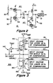
- FIGURE 2 depicts certain details of the FIGURE 1 A/D converter 10.
- a pair of complementary transistor switches 42 and 44 serve to alternately couple the reference potential and the input potential to a comparator 62 through a coupling capacitor 52 during each cycle.
Abstract
Description
- This invention relates to flash analog-to-digital (A/D) converters, and in particular to an arrangement for reducing the loading of operating signals for the A/D converters.
- The flash type A/D converter simultaneously compares an analog input signal with a plurality of ascending reference potentials to determine the closest match between the two. For example, a 7-bit A/D converter with the overflow bit uses 128 (i.e., 27) comparators for performing the simultaneous comparisons. In A/D converters of the type exemplified by the IC, CA3300, from RCA, each comparator is alternately coupled to a respective one of the aforesaid plurality of reference potentials and the analog input signal through a coupling capacitor. The output of all the comparators connected to the reference potentials having a value less than the input signal exhibit one output state and the remaining comparators exhibit an opposite output state.
- The outputs of the comparators are fed to logic circuitry (e.g., a programmable logic array) which produces a parallel, 7-bit binary code related to the magnitude of the analog input signal.
- During each cycle, various capacitors (e.g., coupling capacitors and the gate and parasitic capacitances of the switching transistors) are discharged and recharged between the respective reference potentials and the input signal. When the input signal is at either extreme of the range of the reference potential levels, maximum current drain is produced on the reference potential ladder and the input signal source. On the other hand, when the input signal is at the midpoint of the reference potential levels, the current drain on the reference ladder and the input signal source is minimized since the various capacitors tend to be charged equally in the opposite directions during each cycle.
- It is desirable to reduce the current drain on the reference ladder and the input signal source, since it introduces non-linearities, and further reduces either the cycle rate of the A/D converter or decreases the accuracy of the converter for a fixed cycle rate.
- U. S. Patent No. 4,507,649, issued to Dingwall, et al., discloses one approach to the above- mentioned problem of heavy current drain. In the Dingwall et al. approach, a field effect transistor (i.e., FET) is connected in series between each of the plurality of coupling capacitors and the input signal bus. The gate electrodes of the FET's are biased at D. C. potentials which are tailored to the relative position of the respective FET's along the reference ladder. The FET's are constrained to operate in the source follower mode with the various capacitors as the respective load elements for certain ranges of the input signal, so that the individual coupling capacitors cannot charge or discharge to a potential exceeding the respective FET's D.C. gate potential minus its threshold potential, and thereby reducing the loading on the reference ladder.
- This invention discloses yet another concept for reducing loading. In accordance with the present invention, the input signal is tested to determine if it is above or below the midpoint of the reference potential levels. If the input signal is above the midpoint, a lower group of comparators (e.g., lower 25%) receive a fixed lower voltage (e.g., 0.25 VREF), instead of the input signal. On the other hand, if the input signal is below the midpoint, an upper group of comparators (e.g., upper 25%) are provided with a fixed higher voltage (e.g., 0.75 VREF), instead of the input signal.
- In the accompanying drawings:
- FIGURE 1 is a block diagram of a known 7-bit flash analog-to-digital converter;
- FIGURE 2 illustrates certain details of the A/D converter of FIGURE 1; and
- FIGURE 3 shows a modification to the FIGURE 1 A/D converter in accordance with the subject invention.
- Referring to FIGURE 1, a representative flash A/
D converter 10 is shown, which is capable of producing a parallel sevenbit output signal 12. The A/D converter 10 is generally of the type disclosed in the afore-mentioned U. S. Patent No. 4,507,649, issued to Dingwall, et al. The seven bit output signal corresponds to the division of the maximum permitted input signal (i.e., VREF) into 128 (or 27) equally-spaced, ascending values. This is accomplished by applying a known voltage VREF, from asource 20, across alinear resistor ladder 22, and tapping the potential across theresistor 22 at 128 equispaced intervals. - The 128 taps provide increasing reference voltages.
- The analog input signal is made available on the
input bus 32 connected to aninput signal source 30. A plurality ofswitches 40 alternately apply the input signal and the respective reference voltages to thecomparators 60 through the associatedcoupling capacitors 50 during each cycle. The outputs of all thecomparators 60 connected to the reference voltages having values less than the input voltage experience one output state (e.g., logical high), and the remaining comparators exhibit a second output state (e.g., logical low). - The
comparators 60 are clocked to sample and compare the input signal at prescribed intervals. At the end of the sampling period, the output states of thecomparators 60 are stored in therespective latches 70. - The outputs of the
latches 70 are applied to the respective 3-input ANDgates 80. Each of theAND gates 80 examines triplets of successive ascending comparator states during every cycle. TheAND gates 80 generate a logical high output signal only for the condition that two adjacent latches connected to a particular AND gate are exhibiting a logical "high" output state and the next ascending latch is exhibiting a logical "low" output state. This arrangement of the AND gates senses the transition point in the output states of thecomparators 60, and produces only a single logical "high" output state for a given input signal. - The outputs of the
AND gates 80 are fed to a programmable logic array (or PLA) 90, which generates a parallel 7-bit output signal 12 corresponding to the particular AND gate currently exhibiting a logical "high" output state. - FIGURE 2 depicts certain details of the FIGURE 1 A/
D converter 10. A pair ofcomplementary transistor switches comparator 62 through acoupling capacitor 52 during each cycle. - The
comparator 62 is in the form of a self- biased CMOS inverter comprising a P-type and an N-type field effect transistor (FET's) 64 and 66 respectively. The FET's 64 and 66 have their respective conduction paths connected together in series between a source of positive potential (VDD) and the ground potential. The gate electrodes of the FET's 64 and 66 are joined together to provide a common input terminal. The output signal of the FET's 64 and 66 is derived from the common junction of the respective conductive paths. Acomplementary transistor switch 68, comprising a P-type and a N-type MOS device, selectively connects the inverter output terminal to the inverter input terminal in response to a pair of complementary control signals ϕ and ϕ. This biases theinverter 62 at its switch or midpoint, with the bias potential being stored on thecoupling capacitor 52. - During an equilibration period, the inverter output potential is fed back to one of the plates of the
coupling capacitor 52. A secondcomplementary switch 42, responsive to the same control signalsφ and φ, couples the reference potential to the other plate of thecoupling capacitor 52. Theswitches inverter 62 biased at it operating potential (i.e., VDD/2) and also leaving thecoupling capacitor 52 charged to the level of the difference between the reference potential and the inverter operating potential. - After the
switches complementary transistor switch 44 connects the input voltage to thecoupling capacitor 52 in response to a second pair of complementary control signals T' and ϕ'. The timings of these first and second control signals are such that theswitches switch 44. The difference between the input voltage and the reference voltage is coupled across thecapacitor 52 to theinverter 62. If the reference voltage applied to theinverter 62 is less than the input voltage, it exhibits a "high" logical output state, and vice versa. The output of theinverter 62 is stored in thelatch 72 as the control signal ϕ' goes low. - During each sampling interval, the various capacitors (i.e., coupling capacitors and the gate and parasitic capacitances of the switching transistors) are alternately charged and discharged between the respective reference voltages and the input voltage. If the input voltage coupled to the capacitors during one sampling interval is at the high end of the range of reference potentials (i.e., VREF), then during the next sampling interval, substantially all the capacitors will be discharged to reference potentials lower than the input voltage and then recharged back to the input voltage near the maximum reference potential VREF. This produces a heavy current drain on the reference
potential source 20 and theinput signal source 30. It is noted that most of the current drain is wastefully produced at the reference potential taps on theladder 22, which are furthest from the tap which matches the input potential. On the other hand, very little current drain results at the reference potential taps near the tap with the reference potential matching the input potential. Heavy current drain also occurs when the input voltage is near the ground potential for similar reasons. On the other hand, when the input voltage is near the midpoint of the reference potential levels, only moderate current drain is imposed on thereference potential ladder 22 and theinput signal source 30. - Pursuant to the present invention, the A/
D converter 10 is modified as shown in FIGURE 3 to substantially reduce the current drain on thereference ladder 22 and theinput signal source 30 by not applying input signals to thosecomparators 60 which are well removed from the reference-tap matching the input potential. Thecomparators 60 are illustratively grouped in 3 groups in correspondence with the ranges of reference potentials to which they are connected. In this particular embodiment, the upper, middle and lower groups ofcomparators middle 50%, and thebottom 25% of the reference potential taps. The input signal is selectively made available to the upper and lower groups ofcomparators comparators 120. It will be noted that the choice of three groups of comparators in the particular embodiment described herein is arbitrary. - The
modification 100, in accordance with the instant invention, includes means 140, which tests the input signal and develops a control signal depending upon the input signal being above or below the midpoint of the reference potentials. The midpoint sensing means 140 is a threshold detector which develops a logical "low" control potential when the input signal is greater than VREF/2 and a logical "high" control potential when the input signal is less than VREF/2. The control signal on theoutput terminal 142 of the midpoint sensing means 140 is fed to first and second switching means 150 and 160 for selectively applying either the input signal or an appropriate fixed potential (e.g., 0.75 VREF and 0.25 VREF) to the upper and lower groups ofcomparators - The first switching means 150 comprises first and second transistor switches 152 and 154 (e.g., FET's). The
first transistor switch 152 has its conduction path connected in series between a relatively high fixed voltage (e.g., 0.75 VREF) and the signal input terminal 156 of the upper group ofcomparators 110. The control signal on the terminal 142 is applied to the control electrode of thefirst transistor switch 152. Thesecond transistor switch 154 has its conduction path coupled in series between theinput signal source 30 and the input terminal 156 of the upper group ofcomparators 110. The control signal on the terminal 142 is applied to the control electrode of thesecond transistor switch 154 through aninverter 158. The transistor switches 152 and 154 are arranged to operate in a complementary fashion. When the input signal is above the midpoint reference potential, the control signal on the terminal 142 serves to open thefirst transistor switch 152, and to close thesecond transistor switch 154 to couple the input signal from thesource 30 to the input terminal 156 of the upper group of comparators. Alternatively, when the input signal is below the midpoint reference potential, thefirst transistor switch 152 connects the relatively high fixed voltage (0.75 VREF) to the input terminal 156 of the upper group ofcomparators 110 and thesecond transistor switch 154 blocks off the input signal from thesource 30 from being applied to the upper group. In other words, this arrangement precludes all the capacitors (i.e., coupling, gate and parasitic) associated with the upper group ofcomparators 110 from discharging to the relatively low input signal level when the input signal is below the midpoint reference potential, whereby unnecessary heavy current drain on thereference ladder 22 and theinput signal source 30 is avoided. - Similarly, the second switching means 160, consists of third and fourth transistor switches 162 and 164 (e.g., FET's), which serve to selectively couple the
input signal source 30 to theinput terminal 166 of the lower group ofcomparators 130 when the input signal is below the midpoint reference potential. When the input signal is above the midpoint reference potential, thethird transistor switch 162 is turned on to feed the relatively low fixed voltage (0.25 VREF) to theinput terminal 166 of the lower group ofcomparators 130, and the fourth transistor switch 164 is switched off to isolate theinput signal source 30 from the lower group. Thus, the second switching means 160 prevents all the capacitors (i.e., coupling, gate and parasitic) associated with the lower group ofcomparators 130 from charging to the relatively high input signal level when the input signal is above the midpoint reference potential, thereby again reducing the current drain on thereference ladder 22 and theinput signal source 30. - Thus, in accordance with this invention, the input signal is continuously monitored, and depending upon whether the input signal is above or below the midpoint reference potential, a fixed potential, in lieu of the input signal, is supplied to the remotest comparators which drain heavy input current. This strategy can typically reduce the input current drain to about 25 to 30% range. As long as the input voltage monitoring can be made sufficiently fast, the net result will be to substantially reduce the current drain on the reference ladder without sacrificing accuracy of the analog-to-digital conversion process.
- Although, in the particular embodiment described herein, the comparators are divided into three groups, it will be appreciated that the comparators may be divided into two or more groups, and the current drain on the reference voltage ladder and the input signal source can be reduced by disabling the input signals to the comparators that are well removed from the tap with a reference potential matching the input signal.
Claims (6)
Priority Applications (1)
| Application Number | Priority Date | Filing Date | Title |
|---|---|---|---|
| AT86304682T ATE59747T1 (en) | 1985-06-28 | 1986-06-17 | LOAD LIMITING DEVICE FOR AD CONVERTERS WORKING ACCORDING TO THE PARALLEL PROCESS. |
Applications Claiming Priority (2)
| Application Number | Priority Date | Filing Date | Title |
|---|---|---|---|
| US749858 | 1985-06-28 | ||
| US06/749,858 US4602241A (en) | 1985-06-28 | 1985-06-28 | Input current saving apparatus for flash A/D converter |
Publications (3)
| Publication Number | Publication Date |
|---|---|
| EP0208437A2 EP0208437A2 (en) | 1987-01-14 |
| EP0208437A3 EP0208437A3 (en) | 1988-09-28 |
| EP0208437B1 true EP0208437B1 (en) | 1991-01-02 |
Family
ID=25015512
Family Applications (1)
| Application Number | Title | Priority Date | Filing Date |
|---|---|---|---|
| EP86304682A Expired - Lifetime EP0208437B1 (en) | 1985-06-28 | 1986-06-17 | Load limiting apparatus for flash a/d converter |
Country Status (12)
| Country | Link |
|---|---|
| US (1) | US4602241A (en) |
| EP (1) | EP0208437B1 (en) |
| JP (1) | JPS626537A (en) |
| KR (1) | KR930007720B1 (en) |
| AT (1) | ATE59747T1 (en) |
| AU (1) | AU578369B2 (en) |
| CA (1) | CA1245364A (en) |
| DD (1) | DD248010A5 (en) |
| DE (1) | DE3676365D1 (en) |
| DK (1) | DK308186A (en) |
| ES (1) | ES8800540A1 (en) |
| FI (1) | FI862638A (en) |
Families Citing this family (15)
| Publication number | Priority date | Publication date | Assignee | Title |
|---|---|---|---|---|
| US4924225A (en) * | 1988-01-28 | 1990-05-08 | Harris Semiconductor Patents, Inc. | Analog to digital converter with integral linearity error compensation and method of operation |
| US4870417A (en) * | 1988-02-12 | 1989-09-26 | North American Philips Corporation, Signetics Division | Error correction circuit suitable for thermometer or circular code |
| IT1235679B (en) * | 1989-01-25 | 1992-09-21 | Sgs Thomson Microelectronics | INTEGRATED PROGRAMMABLE MIXED, LOGIC AND ANALOG TYPE. |
| US4918449A (en) * | 1989-02-13 | 1990-04-17 | National Semiconductor Corporation | Multistep flash analog to digital converter with voltage estimator |
| DE4005037A1 (en) * | 1990-02-16 | 1991-08-22 | Siemens Nixdorf Inf Syst | Analogue=digital voltage converter - uses binary values representing results of successive comparisons with respective reference voltages |
| US5404143A (en) * | 1991-06-12 | 1995-04-04 | Intellectual Property Development Associates Of Connecticut, Inc. | Network swappers and circuits constructed from same |
| US5202687A (en) * | 1991-06-12 | 1993-04-13 | Intellectual Property Development Associates Of Connecticut | Analog to digital converter |
| US5231399A (en) * | 1991-09-27 | 1993-07-27 | Trw Inc. | Differential quantizer reference resistor ladder for use with an analog-to-digital converter |
| DE69216818T2 (en) * | 1992-06-03 | 1997-07-24 | Alcatel Bell Nv | Analog to digital converter |
| KR0138029B1 (en) * | 1993-06-07 | 1998-05-15 | 가나이 쯔또무 | Ad converter and magnetic recording/regenerating apparatus using thereor |
| US6002356A (en) * | 1997-10-17 | 1999-12-14 | Microchip Technology Incorporated | Power saving flash A/D converter |
| US6081219A (en) * | 1998-05-05 | 2000-06-27 | Lucent Technology, Inc. | Power saving arrangement for a flash A/D converter |
| US6703960B2 (en) * | 2002-06-20 | 2004-03-09 | Agilent Technologies, Inc. | Analog-to-digital converter |
| US20060114140A1 (en) * | 2004-11-29 | 2006-06-01 | Taiwan Semiconductor Manufacturing Co., Ltd. | Two step flash analog to digital converter |
| KR100945740B1 (en) * | 2007-10-04 | 2010-03-08 | 고려대학교 산학협력단 | A method and apparatus for converting an analog signal to a digital signal |
Family Cites Families (7)
| Publication number | Priority date | Publication date | Assignee | Title |
|---|---|---|---|---|
| US4417233A (en) * | 1979-02-28 | 1983-11-22 | Matsushita Electric Industrial Co., Ltd. | Fully parallel threshold type analog-to-digital converter |
| JPS5947893B2 (en) * | 1979-02-28 | 1984-11-22 | 松下電器産業株式会社 | Parallel analog to digital converter |
| GB2082410B (en) * | 1980-08-23 | 1984-08-30 | Plessey Co Ltd | Analogue-to-digital converter |
| EP0054079B1 (en) * | 1980-12-11 | 1984-09-12 | Deutsche ITT Industries GmbH | Mos-parallel a/d converter |
| US4449118A (en) * | 1981-11-30 | 1984-05-15 | Rca Corporation | Switching circuitry as for a flash A/D converter |
| US4507649A (en) * | 1982-05-24 | 1985-03-26 | Rca Corporation | Flash A/D converter having reduced input loading |
| JPS6072324A (en) * | 1983-09-29 | 1985-04-24 | Toshiba Corp | Analog-to-digital converter |
-
1985
- 1985-06-28 US US06/749,858 patent/US4602241A/en not_active Expired - Fee Related
-
1986
- 1986-06-11 CA CA000511371A patent/CA1245364A/en not_active Expired
- 1986-06-17 DE DE8686304682T patent/DE3676365D1/en not_active Expired - Fee Related
- 1986-06-17 AT AT86304682T patent/ATE59747T1/en not_active IP Right Cessation
- 1986-06-17 EP EP86304682A patent/EP0208437B1/en not_active Expired - Lifetime
- 1986-06-19 FI FI862638A patent/FI862638A/en not_active Application Discontinuation
- 1986-06-20 ES ES556339A patent/ES8800540A1/en not_active Expired
- 1986-06-26 AU AU59283/86A patent/AU578369B2/en not_active Ceased
- 1986-06-27 KR KR1019860005186A patent/KR930007720B1/en not_active IP Right Cessation
- 1986-06-27 DD DD86291802A patent/DD248010A5/en not_active IP Right Cessation
- 1986-06-27 JP JP61152594A patent/JPS626537A/en active Pending
- 1986-06-27 DK DK308186A patent/DK308186A/en not_active Application Discontinuation
Also Published As
| Publication number | Publication date |
|---|---|
| EP0208437A2 (en) | 1987-01-14 |
| FI862638A0 (en) | 1986-06-19 |
| ATE59747T1 (en) | 1991-01-15 |
| CA1245364A (en) | 1988-11-22 |
| KR870000806A (en) | 1987-02-20 |
| ES556339A0 (en) | 1987-10-16 |
| FI862638A (en) | 1986-12-29 |
| JPS626537A (en) | 1987-01-13 |
| AU5928386A (en) | 1987-01-08 |
| DK308186A (en) | 1986-12-29 |
| KR930007720B1 (en) | 1993-08-18 |
| AU578369B2 (en) | 1988-10-20 |
| DD248010A5 (en) | 1987-07-22 |
| ES8800540A1 (en) | 1987-10-16 |
| EP0208437A3 (en) | 1988-09-28 |
| US4602241A (en) | 1986-07-22 |
| DK308186D0 (en) | 1986-06-27 |
| DE3676365D1 (en) | 1991-02-07 |
Similar Documents
| Publication | Publication Date | Title |
|---|---|---|
| EP0208437B1 (en) | Load limiting apparatus for flash a/d converter | |
| US4507649A (en) | Flash A/D converter having reduced input loading | |
| US4907002A (en) | Successive approximation analog to digital converter | |
| US7903018B2 (en) | Analog/digital converter assembly and corresponding method | |
| KR900000997B1 (en) | Intermeshed resistor network for analogue to digital conversion | |
| US4348658A (en) | Analog-to-digital converter using half range technique | |
| US6567029B2 (en) | Low voltage analog-to-digital converters with internal reference voltage and offset | |
| KR20060119780A (en) | Apparatus and method for detecting voltage of assembled battery | |
| CA1097810A (en) | Charge-transfer binary search generating circuit | |
| US4237390A (en) | Switching comparator | |
| US6486816B2 (en) | CDAC operation at low supply voltages | |
| US4973975A (en) | Initial potential setting circuit for a sample/hold circuit associated with an A/D converter | |
| US5075688A (en) | Binary signal generating circuit with parallel sample and hold circuits and common sampling switch | |
| US4897658A (en) | Analog-to-digital converter of successive-approximation type | |
| KR910009067B1 (en) | Analog to digital converter | |
| US4368457A (en) | Analog-to-digital converter | |
| US4929848A (en) | High accuracy reference ladder | |
| US6310572B1 (en) | Semiconductor integrated circuit having plural input control circuits | |
| US4821036A (en) | Method of and apparatus for producing a digital indication of the time-integral of an electric current | |
| US5153454A (en) | Chopper type comparator | |
| US3982140A (en) | High speed bistable multivibrator circuit | |
| EP0067544B1 (en) | Analog-to-digital converter | |
| US7187319B1 (en) | Bulk-compensated sampling network for wide range of signals | |
| US5568148A (en) | Analog/digital conversion circuit | |
| JPH0365685B2 (en) |
Legal Events
| Date | Code | Title | Description |
|---|---|---|---|
| PUAI | Public reference made under article 153(3) epc to a published international application that has entered the european phase |
Free format text: ORIGINAL CODE: 0009012 |
|
| AK | Designated contracting states |
Kind code of ref document: A2 Designated state(s): AT DE FR GB IT NL SE |
|
| RAP1 | Party data changed (applicant data changed or rights of an application transferred) |
Owner name: RCA LICENSING CORPORATION |
|
| PUAL | Search report despatched |
Free format text: ORIGINAL CODE: 0009013 |
|
| AK | Designated contracting states |
Kind code of ref document: A3 Designated state(s): AT DE FR GB IT NL SE |
|
| 17P | Request for examination filed |
Effective date: 19890301 |
|
| 17Q | First examination report despatched |
Effective date: 19900427 |
|
| GRAA | (expected) grant |
Free format text: ORIGINAL CODE: 0009210 |
|
| AK | Designated contracting states |
Kind code of ref document: B1 Designated state(s): AT DE FR GB IT NL SE |
|
| REF | Corresponds to: |
Ref document number: 59747 Country of ref document: AT Date of ref document: 19910115 Kind code of ref document: T |
|
| ITF | It: translation for a ep patent filed |
Owner name: ING. C. GREGORJ S.P.A. |
|
| REF | Corresponds to: |
Ref document number: 3676365 Country of ref document: DE Date of ref document: 19910207 |
|
| ET | Fr: translation filed | ||
| PGFP | Annual fee paid to national office [announced via postgrant information from national office to epo] |
Ref country code: SE Payment date: 19910506 Year of fee payment: 6 |
|
| PGFP | Annual fee paid to national office [announced via postgrant information from national office to epo] |
Ref country code: AT Payment date: 19910627 Year of fee payment: 6 |
|
| PGFP | Annual fee paid to national office [announced via postgrant information from national office to epo] |
Ref country code: NL Payment date: 19910630 Year of fee payment: 6 |
|
| PLBE | No opposition filed within time limit |
Free format text: ORIGINAL CODE: 0009261 |
|
| STAA | Information on the status of an ep patent application or granted ep patent |
Free format text: STATUS: NO OPPOSITION FILED WITHIN TIME LIMIT |
|
| 26N | No opposition filed | ||
| PG25 | Lapsed in a contracting state [announced via postgrant information from national office to epo] |
Ref country code: AT Effective date: 19920617 |
|
| PG25 | Lapsed in a contracting state [announced via postgrant information from national office to epo] |
Ref country code: SE Effective date: 19920618 |
|
| PG25 | Lapsed in a contracting state [announced via postgrant information from national office to epo] |
Ref country code: NL Effective date: 19930101 |
|
| NLV4 | Nl: lapsed or anulled due to non-payment of the annual fee | ||
| PGFP | Annual fee paid to national office [announced via postgrant information from national office to epo] |
Ref country code: FR Payment date: 19940426 Year of fee payment: 9 Ref country code: DE Payment date: 19940426 Year of fee payment: 9 |
|
| PGFP | Annual fee paid to national office [announced via postgrant information from national office to epo] |
Ref country code: GB Payment date: 19940523 Year of fee payment: 9 |
|
| EUG | Se: european patent has lapsed |
Ref document number: 86304682.7 Effective date: 19930109 |
|
| PG25 | Lapsed in a contracting state [announced via postgrant information from national office to epo] |
Ref country code: GB Effective date: 19950617 |
|
| GBPC | Gb: european patent ceased through non-payment of renewal fee |
Effective date: 19950617 |
|
| PG25 | Lapsed in a contracting state [announced via postgrant information from national office to epo] |
Ref country code: FR Effective date: 19960229 |
|
| PG25 | Lapsed in a contracting state [announced via postgrant information from national office to epo] |
Ref country code: DE Effective date: 19960301 |
|
| REG | Reference to a national code |
Ref country code: FR Ref legal event code: ST |
|
| PG25 | Lapsed in a contracting state [announced via postgrant information from national office to epo] |
Ref country code: IT Free format text: LAPSE BECAUSE OF NON-PAYMENT OF DUE FEES Effective date: 20050617 |