EP0206580A2 - Method and apparatus for interconnecting processors in a hyper-dimensional array - Google Patents
Method and apparatus for interconnecting processors in a hyper-dimensional array Download PDFInfo
- Publication number
- EP0206580A2 EP0206580A2 EP86304237A EP86304237A EP0206580A2 EP 0206580 A2 EP0206580 A2 EP 0206580A2 EP 86304237 A EP86304237 A EP 86304237A EP 86304237 A EP86304237 A EP 86304237A EP 0206580 A2 EP0206580 A2 EP 0206580A2
- Authority
- EP
- European Patent Office
- Prior art keywords
- integrated circuits
- dimensions
- backplane
- nearest neighbors
- interconnecting
- Prior art date
- Legal status (The legal status is an assumption and is not a legal conclusion. Google has not performed a legal analysis and makes no representation as to the accuracy of the status listed.)
- Withdrawn
Links
Images
Classifications
-
- G—PHYSICS
- G06—COMPUTING OR CALCULATING; COUNTING
- G06F—ELECTRIC DIGITAL DATA PROCESSING
- G06F13/00—Interconnection of, or transfer of information or other signals between, memories, input/output devices or central processing units
- G06F13/38—Information transfer, e.g. on bus
- G06F13/40—Bus structure
- G06F13/4063—Device-to-bus coupling
- G06F13/409—Mechanical coupling
-
- G—PHYSICS
- G06—COMPUTING OR CALCULATING; COUNTING
- G06F—ELECTRIC DIGITAL DATA PROCESSING
- G06F15/00—Digital computers in general; Data processing equipment in general
- G06F15/16—Combinations of two or more digital computers each having at least an arithmetic unit, a program unit and a register, e.g. for a simultaneous processing of several programs
- G06F15/163—Interprocessor communication
- G06F15/173—Interprocessor communication using an interconnection network, e.g. matrix, shuffle, pyramid, star, snowflake
- G06F15/17337—Direct connection machines, e.g. completely connected computers, point to point communication networks
- G06F15/17343—Direct connection machines, e.g. completely connected computers, point to point communication networks wherein the interconnection is dynamically configurable, e.g. having loosely coupled nearest neighbor architecture
-
- G—PHYSICS
- G06—COMPUTING OR CALCULATING; COUNTING
- G06F—ELECTRIC DIGITAL DATA PROCESSING
- G06F15/00—Digital computers in general; Data processing equipment in general
- G06F15/76—Architectures of general purpose stored program computers
- G06F15/80—Architectures of general purpose stored program computers comprising an array of processing units with common control, e.g. single instruction multiple data processors
Definitions
- This relates to a massively parallel processor- having a large number of interconnected processors operating in parallel and, in particular, to one in which such processors are interconnected in a hyper-dimensional pattern (i.e., a pattern of more than three dimensions).
- the processors are connected in a Boolean n-cube where n is relatively large (e.g. n>10).
- the entire array 30 contains 1,048,576 ( 8 2 20 ) identical processor/memories 36.
- Processor/memories 36 are organized and interconnected in two geometries. The first is a conventional two-dimensional grid pattern in which the processor/memories are organized in a square array and connected to their four nearest neighbors in the array. The second is a Boolean n-cube of fifteen dimensions.
- the present invention is related to the realization of the second of these interconnection geometries in the three-dimensional world of integrated circuits, circuit boards and backplanes (or mother boards) in which it must be built.
- the position of an object in a two dimensional grid by using two numbers, one of which specifies its position in the first dimension of the two-dimensional grid and the other which specifies its position in the second dimension, so too we can use a number to identify the position of an IC in each of the fifteen dimensions of the Boolean 15-cube.
- an IC can have one of only two different positions, 0 and 1, in each dimension.
- the fifteen-digit IC address in binary notation as set forth in Table I also specifies the IC 's'position in the fifteen dimensions of the n-cube.
- each IC has fifteen other ICs whose binary address differs by only one digit from its own address.
- We will refer to these fifteen ICs whose address differs by only one from that of a first IC as the first IC's nearest neighbors.
- Those familiar with the mathematical definition of a Hamming distance will recognize that the first IC is separated from each of its fifteen nearest neighbors by the Hamming distance one.
- Two examples of the addresses of an IC and its fifteen nearest neighbors are set forth in Table II of the above referenced applications. With reference to Table I of the present application, the ICs whose decimal address are 1, 2 and 4 are some of the nearest neighbors of the IC whose decimal address is 0.
- each IC is connected to its fifteen nearest neighbors by 15 input lines 38 and fifteen output lines 39.
- Each of these fifteen input lines 38 to each IC 35 is associated with a different one of the fifteen dimensions of the Boolean 15-cube and likewise each of the fifteen output lines 39 from each IC 35 is associated with a different dimension.
- the results of computations are organized in the form of message packets; and these packets are routed from one IC to the next by routing circuitry in each IC in accordance with address information that is part of the packet.
- An illustrative format of the message packet is depicted in Fig. 4 of the above-identified application where it is seen to comprise fifteen bits of IC address, a format bit, another fifteen bits duplicating the IC address, five bits of address to the processor/memory in the IC, four bits of address to a register in the processor/memory, thirty-two bits of a message and one bit for error detection.
- a message packet can be used that employs only one set of fifteen bits for an IC address.
- the IC address information is relative to the address of the destination IC. Initially, it is the difference or the displacement between the address of the IC that is the source of the message and that of its destination. For example, if the address of the source IC is 010 101 010 101 010 and the address of the destination IC is 111 111 111 111 111, then the relative address that is generated at the source IC is 101 010 101 010 101. It will be apparent that 1-bits in the relative address identify the dimensions where the message packet is not in the correct position and therefore identify the dimensions through which the message packet must be moved to reach the destination IC.
- the message is already located in the proper position in those dimensions.
- the presence of 1-bits in the relative address for those dimensions indicates that it is necessary to move the message packet from one IC to another in that dimension.
- the relative address is updated to take into account each move.
- the message packet includes a . duplicate IC address
- this is conveniently done by complementing the bits in the duplicate IC address that are associated with the dimensions through which the message packet is moved.
- the bits in the duplicate IC address will be all zeros.
- the routing circuitry in all the ICs is identical and operates in synchronism using the same routing cycle.
- the routing circuitry at each IC in the Boolean n-cube tests the leading bit of the first copy of the IC address of each message packet in the routing circuitry to determine its level. If there is a 1-bit in this position and if the output line from that IC which is associated with the first dimension is not already busy, the message packet is routed down the first dimension output line to the IC's nearest neighbor in the first dimension. If the leading bit of the message packet address is a 0-bit, the message packet remains in the same IC because it is in the correct position in the first dimension.
- the leading bit of the first copy of the IC address in the message packet is then discarded. If the message packet was routed to another IC, the corresponding address-bit in the duplicate IC address is complemented in order to account for such move.
- the process is the same, but the bits of the IC address are not discarded after use in routing selection. Rather, the bit associated with each dimension is complemented if the message packet was routed to another IC in that dimension and the entire address, as complemented, is retained. Again, when all fifteen bits of address are zero, the message packet has reached its destination.
- the nearest neighbors of each integrated circuit chip are located on circuit boards and backplanes (or mother boards) so that:
- each integrated circuit on a circuit board is connected to five integrated circuits on the same board which are its nearest neighbors in the first five dimensions. Further, each integrated circuit is also connected to four other integrated circuits on different circuit boards, but on the same backplane. Finally, each integrated circuit is also connected to three other integrated circuits, each on a different backplane.
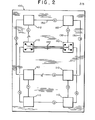
- Fig. 2 depicts the layout of a circuit board 100 in accordance with the invention.
- board 100 is divided into eight identical sections 110 and each section contains four integrated circuits 120.
- each integrated circuit contains sixteen processor/memory circuits.
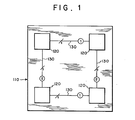
- Fig. 1 shows in greater detail one of sections 110 and in particular, depicts the connections in the first and second dimensions between the four integrated circuits 120 of that section.
- Each integrated circuit is connected by lines 130 to two other integrated circuits which are its nearest neighbors in the first and second dimensions.
- each line 130 represents one or more input and output lines of each IC chip, circuit board or backplane to which it is connected.
- the number of such lines is signified by a number following a slash through the line; and the dimension associated with the line is specified within a bubble in the line.
- Fig. 2 depicts the connections between the sections.
- each section 110 is seen to be connected to three other sections; and as shown in the detailed portion of Fig. 2, each integrated circuit of a section is connected to one integrated circuit in each section to which the section is connected.
- each integrated circuit is connected to its nearest neighbors in the third, fourth and fifth dimensions.
- Fig. 2 Examination of the layout of Fig. 2 will reveal a connection pattern that is the same as the connection pattern that would be observed if each of the eight sections were located at a different vertex of a cube.
- the four sections in the upper half of Fig. 2 can be regarded as the four sections in the four corners of the base of a cube; and the four sections in the lower half of Fig. 2 can be regarded as the four sections in the four corners of the top of the cube.
- each section in the upper half is connected to its two nearest neighbors in that half; and likewise each section in the lower half is connected to its two nearest neighbors in the lower half.
- each section in the upper half of Fig. 2 is also connected to one section in the lower half and that section is the section that is its nearest neighbor in the top of the cube.
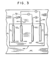
- the circuit boards are organized in sets and mounted on a backplane 140 shown in Figs. 3 and 4.
- Each set comprises four circuit boards 120 which are interconnected by lines 130 so that each board is connected to two of the other three boards in the-set.
- each IC on a board is connected to one IC on each of two of the other boards, thereby providing connections to three of its nearest neighbors in the sixth and seventh dimensions.
- each IC on a board is connected to one IC on each of two of the other three sets, thereby providing connections to its nearest neighbors in the eighth and ninth dimensions.
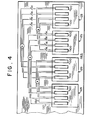
- the backplanes are mounted in racks 150, with an upper backplane and a lower backplane in each rack.
- the ICs of each backplane are connected by lines 130 to those in the three nearest backplanes so that each IC in each backplane is connected to an IC in each of three other backplanes, thereby providing connections to its nearest neighbors in the tenth, eleventh and twelfth dimensions.
- connection pattern can be generalized from the foregoing description.
- the ICs on each circuit board are connected to those ICs which are its nearest neighbors in dimensions 1 through L; the ICs on the boards connected to a backplane are connected to those ICs on other boards on the same backplane which are its nearest neighbors in dimensions L+l through M; and the ICs on a backplane are connected to those ICs on other backplanes that are its nearest neighbors in dimensions M+l through N.
- the ICs on a circuit board are connected to those ICs which are its nearest neighbors in a first consecutive number of dimensions; those on boards connected to a backplane are connected to ICs on other boards connected to the same backplane that are its nearest neighbors in a second consecutive number of dimensions; and those on a backplane are connected to ICs on other backplanes that are its nearest neighbors in a third consecutive number of dimensions.
Landscapes
- Engineering & Computer Science (AREA)
- Computer Hardware Design (AREA)
- Theoretical Computer Science (AREA)
- General Engineering & Computer Science (AREA)
- Physics & Mathematics (AREA)
- General Physics & Mathematics (AREA)
- Mathematical Physics (AREA)
- Software Systems (AREA)
- Computing Systems (AREA)
- Multi Processors (AREA)
Abstract
Description
- This relates to a massively parallel processor- having a large number of interconnected processors operating in parallel and, in particular, to one in which such processors are interconnected in a hyper-dimensional pattern (i.e., a pattern of more than three dimensions). Advantageously, the processors are connected in a Boolean n-cube where n is relatively large (e.g. n>10).
- As described in connection with Fig. 1A of the above-referenced application an array 30 of parallel processing integrated circuits (ICs) 35, illustratively, contains 32,768 (=215) identical ICs 35; and each IC 35 contains 32 (=25) identical processor/memories 36. Thus the entire array 30 contains 1,048,576 (8220) identical processor/memories 36. Processor/memories 36 are organized and interconnected in two geometries. The first is a conventional two-dimensional grid pattern in which the processor/memories are organized in a square array and connected to their four nearest neighbors in the array. The second is a Boolean n-cube of fifteen dimensions.
- The present invention is related to the realization of the second of these interconnection geometries in the three-dimensional world of integrated circuits, circuit boards and backplanes (or mother boards) in which it must be built.
- To understand the n-cube connection pattern for ICs 35, it is helpful to number the ICe from 0 to 32,767 and to express these numbers or addresses in binary notation using fifteen binary digits as in Table I.

- Just as we can specify the position of an object in a two dimensional grid by using two numbers, one of which specifies its position in the first dimension of the two-dimensional grid and the other which specifies its position in the second dimension, so too we can use a number to identify the position of an IC in each of the fifteen dimensions of the Boolean 15-cube. In an n-cube, however, an IC can have one of only two different positions, 0 and 1, in each dimension. Thus, the fifteen-digit IC address in binary notation as set forth in Table I also specifies the IC's'position in the fifteen dimensions of the n-cube. For convenience, we will use the left-hand-most digit of the fifteen binary digits to specify the IC's position in the first dimension, and so on in order to the right-hand-most digit which specifies the IC's position in the fifteenth dimension.
- Moreover, because a binary digit can have only two values, zero or one, and because each IC is identified uniquely by fifteen binary digits, each IC has fifteen other ICs whose binary address differs by only one digit from its own address. We will refer to these fifteen ICs whose address differs by only one from that of a first IC as the first IC's nearest neighbors. Those familiar with the mathematical definition of a Hamming distance will recognize that the first IC is separated from each of its fifteen nearest neighbors by the Hamming distance one. Two examples of the addresses of an IC and its fifteen nearest neighbors are set forth in Table II of the above referenced applications. With reference to Table I of the present application, the ICs whose decimal address are 1, 2 and 4 are some of the nearest neighbors of the IC whose decimal address is 0.
- To connect ICs 35 of the above-referenced application in the form of a Boolean 15-cube, each IC is connected to its fifteen nearest neighbors by 15 input lines 38 and fifteen output lines 39. Each of these fifteen input lines 38 to each IC 35 is associated with a different one of the fifteen dimensions of the Boolean 15-cube and likewise each of the fifteen output lines 39 from each IC 35 is associated with a different dimension.
- To permit communication through the interconnection pattern of the Boolean 15-cube, the results of computations are organized in the form of message packets; and these packets are routed from one IC to the next by routing circuitry in each IC in accordance with address information that is part of the packet. An illustrative format of the message packet is depicted in Fig. 4 of the above-identified application where it is seen to comprise fifteen bits of IC address, a format bit, another fifteen bits duplicating the IC address, five bits of address to the processor/memory in the IC, four bits of address to a register in the processor/memory, thirty-two bits of a message and one bit for error detection. Alternatively, a message packet can be used that employs only one set of fifteen bits for an IC address.
- In the message packet, the IC address information is relative to the address of the destination IC. Initially, it is the difference or the displacement between the address of the IC that is the source of the message and that of its destination. For example, if the address of the source IC is 010 101 010 101 010 and the address of the destination IC is 111 111 111 111 111, then the relative address that is generated at the source IC is 101 010 101 010 101. It will be apparent that 1-bits in the relative address identify the dimensions where the message packet is not in the correct position and therefore identify the dimensions through which the message packet must be moved to reach the destination IC. Thus, in the above example, where the addresses of the source and destination ICs are the same in each of the even-numbered dimensions, the message is already located in the proper position in those dimensions. However, in the odd dimensions where the addresses of the source and the destination ICs are different, the presence of 1-bits in the relative address for those dimensions indicates that it is necessary to move the message packet from one IC to another in that dimension.
- As the message is routed from one IC to the next, the relative address is updated to take into account each move. In the case where the message packet includes a . duplicate IC address, this is conveniently done by complementing the bits in the duplicate IC address that are associated with the dimensions through which the message packet is moved. As a result, when the message packet arrives at the destination IC, the bits in the duplicate IC address will be all zeros.
- The routing circuitry in all the ICs is identical and operates in synchronism using the same routing cycle. In the first time period of each routing cycle, the routing circuitry at each IC in the Boolean n-cube tests the leading bit of the first copy of the IC address of each message packet in the routing circuitry to determine its level. If there is a 1-bit in this position and if the output line from that IC which is associated with the first dimension is not already busy, the message packet is routed down the first dimension output line to the IC's nearest neighbor in the first dimension. If the leading bit of the message packet address is a 0-bit, the message packet remains in the same IC because it is in the correct position in the first dimension.
- The leading bit of the first copy of the IC address in the message packet is then discarded. If the message packet was routed to another IC, the corresponding address-bit in the duplicate IC address is complemented in order to account for such move.
- In the second address time period, the routing circuitry of each IC tests the second bit of the relative address which indicates whether the message packet is in the proper position in the second dimension. If the bit is a 1-bit and if the second dimension output line is not already busy, the message packet is then routed out on the second dimension output line to that IC's nearest neighbor in the second dimension. If the bit is a 0-bit, the message packet remains in the 1C.
- This process continues through fifteen address time periods, at the end of which each of the fifteen address bits of the message packet will have been tested; and if the needed output lines were available, a path will have been established through the Boolean 15-cube through which the remainder of the message packet can be transmitted.
- In the case where the message packet contains only a single fifteen-bit IC addres, the process is the same, but the bits of the IC address are not discarded after use in routing selection. Rather, the bit associated with each dimension is complemented if the message packet was routed to another IC in that dimension and the entire address, as complemented, is retained. Again, when all fifteen bits of address are zero, the message packet has reached its destination.
- In accordance with one form of the invention, the nearest neighbors of each integrated circuit chip are located on circuit boards and backplanes (or mother boards) so that:
- 1. all message packets are first routed to nearest neighbor ICs located on the same circuit board;
- 2. all message packets are then routed to nearest neighbor ICs located on the same backplane; and
- 3. all message packets are then routed to nearest neighbor ICs located on different backplanes.
- This is accomplished by interconnecting the ICs on circuit boards and backplanes so that on each circuit board the ICs are connected to their nearest neighbor ICs in a first consecutive number of dimensions, on each backplane the ICs on each board are connected to ICs on other boards of the same backplane that are its nearest neighbors in a second consecutive number of dimensions and the ICs on one backplane are connected to those on other backplanes that are its nearest neighbors in a third consecutive number of dimensions.
- One such massively parallel system that has been implemented in accordance with the invention comprises 65,534 (=216) individual processors organized so that there are 16 (=24) individual processors on each of 4,096 (=212) integrated circuits. In this system each circuit board carries 32 (=25) integrated circuits and each backplane carries 16 (824) circuit boards. There are eight (823) backplanes advantageously arranged in a cube that is 2x2x2.
- In accordance with the invention, each integrated circuit on a circuit board is connected to five integrated circuits on the same board which are its nearest neighbors in the first five dimensions. Further, each integrated circuit is also connected to four other integrated circuits on different circuit boards, but on the same backplane. Finally, each integrated circuit is also connected to three other integrated circuits, each on a different backplane.
- As a result of these arrangements, the effects of different path lengths between nearest neighbor ICs can be minimized by altering the time required for different clock cycles during a routing cycle. Thus, while message packets are being routed to the nearest neighbors on the same board, relatively short clock cycles can be used commeasurate with the relatively short propagation distances encountered. Longer clock cycles can be used during that portion of the routing cycle in which the message packets are routed over the longer distances between backplanes.
- These and other objects, features and advantages of the invention will be more readily apparent from the following detailed description of a preferred embodiment of the invention in which:
- Fig. 1 is a schematic illustration of the interconnection of an IC chip to its nearest neighbors in the first and second dimensions on a circuit board;
- Fig. 2 is a schematic illustration of the interconnection of an IC chip to its nearest neighbors in the third, fourth and fifth dimensions on a circuit board;
- Fig. 3 is a schematic illustration of the interconnection of an IC chip to its nearest neighbors in the sixth and seventh dimensions on a backplane;
- Fig. 4 is a schematic illustration of the interconnection of an IC chip to its nearest neighbors in the eighth and ninth dimensions on a backplane; and
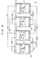
- Fig. 5 is a schematic illustration of the interconnection of an IC chip to its nearest neighbors in the tenth, eleventh and twelfth dimensions on different backplanes.
- Fig. 2 depicts the layout of a
circuit board 100 in accordance with the invention. As shown therein,board 100 is divided into eightidentical sections 110 and each section contains fourintegrated circuits 120. Illustratively, each integrated circuit contains sixteen processor/memory circuits. Fig. 1 shows in greater detail one ofsections 110 and in particular, depicts the connections in the first and second dimensions between the fourintegrated circuits 120 of that section. Each integrated circuit is connected bylines 130 to two other integrated circuits which are its nearest neighbors in the first and second dimensions. - For convenience of illustration each
line 130 represents one or more input and output lines of each IC chip, circuit board or backplane to which it is connected. The number of such lines is signified by a number following a slash through the line; and the dimension associated with the line is specified within a bubble in the line. - Fig. 2 depicts the connections between the sections. Thus, each
section 110 is seen to be connected to three other sections; and as shown in the detailed portion of Fig. 2, each integrated circuit of a section is connected to one integrated circuit in each section to which the section is connected. Thus, each integrated circuit is connected to its nearest neighbors in the third, fourth and fifth dimensions. - Examination of the layout of Fig. 2 will reveal a connection pattern that is the same as the connection pattern that would be observed if each of the eight sections were located at a different vertex of a cube. Thus, the four sections in the upper half of Fig. 2 can be regarded as the four sections in the four corners of the base of a cube; and the four sections in the lower half of Fig. 2 can be regarded as the four sections in the four corners of the top of the cube. As is apparent from Fig. 2, each section in the upper half is connected to its two nearest neighbors in that half; and likewise each section in the lower half is connected to its two nearest neighbors in the lower half. Moreover, each section in the upper half of Fig. 2 is also connected to one section in the lower half and that section is the section that is its nearest neighbor in the top of the cube.
- The circuit boards are organized in sets and mounted on a
backplane 140 shown in Figs. 3 and 4. Each set comprises fourcircuit boards 120 which are interconnected bylines 130 so that each board is connected to two of the other three boards in the-set. By this means, each IC on a board is connected to one IC on each of two of the other boards, thereby providing connections to three of its nearest neighbors in the sixth and seventh dimensions. - In similar fashion, the boards in each set are connected to boards in two of the other three sets so that each IC on a board is connected to one IC on each of two of the other three sets, thereby providing connections to its nearest neighbors in the eighth and ninth dimensions.
- As shown in Fig. 5, the backplanes are mounted in
racks 150, with an upper backplane and a lower backplane in each rack. The ICs of each backplane are connected bylines 130 to those in the three nearest backplanes so that each IC in each backplane is connected to an IC in each of three other backplanes, thereby providing connections to its nearest neighbors in the tenth, eleventh and twelfth dimensions. - This connection pattern can be generalized from the foregoing description. The ICs on each circuit board are connected to those ICs which are its nearest neighbors in
dimensions 1 through L; the ICs on the boards connected to a backplane are connected to those ICs on other boards on the same backplane which are its nearest neighbors in dimensions L+l through M; and the ICs on a backplane are connected to those ICs on other backplanes that are its nearest neighbors in dimensions M+l through N. Even more generally, the ICs on a circuit board are connected to those ICs which are its nearest neighbors in a first consecutive number of dimensions; those on boards connected to a backplane are connected to ICs on other boards connected to the same backplane that are its nearest neighbors in a second consecutive number of dimensions; and those on a backplane are connected to ICs on other backplanes that are its nearest neighbors in a third consecutive number of dimensions. - The foregoing technique can also be extended to other structures. For example, individual processors on a single integrated circuit could also be connected in this same fashion. Thus, if eight processors are located on a chip, each of these processors could be connected through a layout like that of Fig. 2 to its three nearest neighbors in three consecutive dimensions. Most likely such dimensions would be
dimensions
Claims (16)
Applications Claiming Priority (2)
| Application Number | Priority Date | Filing Date | Title |
|---|---|---|---|
| US06/740,943 US4805091A (en) | 1985-06-04 | 1985-06-04 | Method and apparatus for interconnecting processors in a hyper-dimensional array |
| US740943 | 1985-06-04 |
Publications (2)
| Publication Number | Publication Date |
|---|---|
| EP0206580A2 true EP0206580A2 (en) | 1986-12-30 |
| EP0206580A3 EP0206580A3 (en) | 1988-05-18 |
Family
ID=24978704
Family Applications (1)
| Application Number | Title | Priority Date | Filing Date |
|---|---|---|---|
| EP86304237A Withdrawn EP0206580A3 (en) | 1985-06-04 | 1986-06-04 | Method and apparatus for interconnecting processors in a hyper-dimensional array |
Country Status (4)
| Country | Link |
|---|---|
| US (1) | US4805091A (en) |
| EP (1) | EP0206580A3 (en) |
| JP (1) | JPH0833873B2 (en) |
| CA (1) | CA1256581A (en) |
Cited By (6)
| Publication number | Priority date | Publication date | Assignee | Title |
|---|---|---|---|---|
| EP0201797A3 (en) * | 1985-05-06 | 1988-06-01 | Ncube Corporation | High-performance computer system |
| GB2206428A (en) * | 1987-06-15 | 1989-01-05 | Texas Instruments Ltd | Computer |
| WO1990009635A1 (en) * | 1989-02-08 | 1990-08-23 | Yvon Savaria | Parallel microprocessor architecture |
| GB2251320A (en) * | 1990-12-20 | 1992-07-01 | Motorola Ltd | Parallel processor |
| EP0726528A1 (en) * | 1995-02-08 | 1996-08-14 | International Business Machines Corporation | Interconnection network for a multi-nodal data processing system |
| EP2302525A1 (en) * | 2009-09-01 | 2011-03-30 | Fujitsu Limited | Parallel computing system and communication control program |
Families Citing this family (90)
| Publication number | Priority date | Publication date | Assignee | Title |
|---|---|---|---|---|
| US5175865A (en) * | 1986-10-28 | 1992-12-29 | Thinking Machines Corporation | Partitioning the processors of a massively parallel single array processor into sub-arrays selectively controlled by host computers |
| US5170482A (en) * | 1987-08-14 | 1992-12-08 | Regents Of The University Of Minnesota | Improved hypercube topology for multiprocessor computer systems |
| JP2509947B2 (en) * | 1987-08-19 | 1996-06-26 | 富士通株式会社 | Network control system |
| US5105424A (en) * | 1988-06-02 | 1992-04-14 | California Institute Of Technology | Inter-computer message routing system with each computer having separate routinng automata for each dimension of the network |
| US5159690A (en) * | 1988-09-30 | 1992-10-27 | Massachusetts Institute Of Technology | Multidimensional cellular data array processing system which separately permutes stored data elements and applies transformation rules to permuted elements |
| US5041971A (en) * | 1988-11-30 | 1991-08-20 | Bolt Beranek And Newman Inc. | Memory accessing switch network |
| US5243704A (en) * | 1989-05-19 | 1993-09-07 | Stratus Computer | Optimized interconnect networks |
| US5345578A (en) * | 1989-06-30 | 1994-09-06 | Digital Equipment Corporation | Competitive snoopy caching for large-scale multiprocessors |
| US5142629A (en) * | 1989-09-06 | 1992-08-25 | Unisys Corporation | System for interconnecting MSUs to a computer system |
| US5109479A (en) * | 1989-09-07 | 1992-04-28 | Amp-Akzo Corporation | Method of designing three dimensional electrical circuits |
| US5170370A (en) * | 1989-11-17 | 1992-12-08 | Cray Research, Inc. | Vector bit-matrix multiply functional unit |
| AU644141B2 (en) * | 1990-01-05 | 1993-12-02 | Maspar Computer Corporation | A method of controlling a router circuit |
| AU645785B2 (en) * | 1990-01-05 | 1994-01-27 | Maspar Computer Corporation | Parallel processor memory system |
| US5280474A (en) * | 1990-01-05 | 1994-01-18 | Maspar Computer Corporation | Scalable processor to processor and processor-to-I/O interconnection network and method for parallel processing arrays |
| US5133073A (en) * | 1990-05-29 | 1992-07-21 | Wavetracer, Inc. | Processor array of N-dimensions which is physically reconfigurable into N-1 |
| US5157785A (en) * | 1990-05-29 | 1992-10-20 | Wavetracer, Inc. | Process cell for an n-dimensional processor array having a single input element with 2n data inputs, memory, and full function arithmetic logic unit |
| US5193202A (en) * | 1990-05-29 | 1993-03-09 | Wavetracer, Inc. | Processor array with relocated operand physical address generator capable of data transfer to distant physical processor for each virtual processor while simulating dimensionally larger array processor |
| US5377129A (en) * | 1990-07-12 | 1994-12-27 | Massachusetts Institute Of Technology | Particle interaction processing system |
| US5367636A (en) * | 1990-09-24 | 1994-11-22 | Ncube Corporation | Hypercube processor network in which the processor indentification numbers of two processors connected to each other through port number n, vary only in the nth bit |
| US5966528A (en) * | 1990-11-13 | 1999-10-12 | International Business Machines Corporation | SIMD/MIMD array processor with vector processing |
| US5765011A (en) * | 1990-11-13 | 1998-06-09 | International Business Machines Corporation | Parallel processing system having a synchronous SIMD processing with processing elements emulating SIMD operation using individual instruction streams |
| US5617577A (en) * | 1990-11-13 | 1997-04-01 | International Business Machines Corporation | Advanced parallel array processor I/O connection |
| US5625836A (en) * | 1990-11-13 | 1997-04-29 | International Business Machines Corporation | SIMD/MIMD processing memory element (PME) |
| US5734921A (en) * | 1990-11-13 | 1998-03-31 | International Business Machines Corporation | Advanced parallel array processor computer package |
| US5590345A (en) * | 1990-11-13 | 1996-12-31 | International Business Machines Corporation | Advanced parallel array processor(APAP) |
| US5630162A (en) * | 1990-11-13 | 1997-05-13 | International Business Machines Corporation | Array processor dotted communication network based on H-DOTs |
| US5794059A (en) * | 1990-11-13 | 1998-08-11 | International Business Machines Corporation | N-dimensional modified hypercube |
| US5765012A (en) * | 1990-11-13 | 1998-06-09 | International Business Machines Corporation | Controller for a SIMD/MIMD array having an instruction sequencer utilizing a canned routine library |
| US5828894A (en) * | 1990-11-13 | 1998-10-27 | International Business Machines Corporation | Array processor having grouping of SIMD pickets |
| US5963745A (en) * | 1990-11-13 | 1999-10-05 | International Business Machines Corporation | APAP I/O programmable router |
| US5588152A (en) * | 1990-11-13 | 1996-12-24 | International Business Machines Corporation | Advanced parallel processor including advanced support hardware |
| US5765015A (en) * | 1990-11-13 | 1998-06-09 | International Business Machines Corporation | Slide network for an array processor |
| US5752067A (en) * | 1990-11-13 | 1998-05-12 | International Business Machines Corporation | Fully scalable parallel processing system having asynchronous SIMD processing |
| US5963746A (en) * | 1990-11-13 | 1999-10-05 | International Business Machines Corporation | Fully distributed processing memory element |
| US5815723A (en) * | 1990-11-13 | 1998-09-29 | International Business Machines Corporation | Picket autonomy on a SIMD machine |
| US5809292A (en) * | 1990-11-13 | 1998-09-15 | International Business Machines Corporation | Floating point for simid array machine |
| DE69131272T2 (en) * | 1990-11-13 | 1999-12-09 | International Business Machines Corp., Armonk | Parallel associative processor system |
| US5379438A (en) * | 1990-12-14 | 1995-01-03 | Xerox Corporation | Transferring a processing unit's data between substrates in a parallel processor |
| GB9027663D0 (en) * | 1990-12-20 | 1991-02-13 | Sandoz Ltd | Light-stabilizing compositions |
| US5206506A (en) * | 1991-02-12 | 1993-04-27 | Kirchner Nicholas J | Ion processing: control and analysis |
| US5594918A (en) * | 1991-05-13 | 1997-01-14 | International Business Machines Corporation | Parallel computer system providing multi-ported intelligent memory |
| US5442797A (en) * | 1991-12-04 | 1995-08-15 | Casavant; Thomas L. | Latency tolerant risc-based multiple processor with event driven locality managers resulting from variable tagging |
| CA2078912A1 (en) * | 1992-01-07 | 1993-07-08 | Robert Edward Cypher | Hierarchical interconnection networks for parallel processing |
| US5524212A (en) * | 1992-04-27 | 1996-06-04 | University Of Washington | Multiprocessor system with write generate method for updating cache |
| US5581773A (en) * | 1992-05-12 | 1996-12-03 | Glover; Michael A. | Massively parallel SIMD processor which selectively transfers individual contiguously disposed serial memory elements |
| JP2642039B2 (en) * | 1992-05-22 | 1997-08-20 | インターナショナル・ビジネス・マシーンズ・コーポレイション | Array processor |
| US5444701A (en) * | 1992-10-29 | 1995-08-22 | International Business Machines Corporation | Method of packet routing in torus networks with two buffers per edge |
| JPH06290158A (en) * | 1993-03-31 | 1994-10-18 | Fujitsu Ltd | Reconfigurable torus network method |
| US5680536A (en) * | 1994-03-25 | 1997-10-21 | Tyuluman; Samuel A. | Dual motherboard computer system |
| US5544330A (en) * | 1994-07-13 | 1996-08-06 | Emc Corporation | Fault tolerant interconnect topology using multiple rings |
| US5781551A (en) * | 1994-09-15 | 1998-07-14 | Texas Instruments Incorporated | Computer communications system with tree architecture and communications method |
| KR19990036054A (en) * | 1995-07-28 | 1999-05-25 | 세모스 로버트 어니스트 빅커스 | Packet routing method and apparatus |
| US5913070A (en) * | 1996-01-16 | 1999-06-15 | Tm Patents, L.P. | Inter-connector for use with a partitionable massively parallel processing system |
| US6513108B1 (en) | 1998-06-29 | 2003-01-28 | Cisco Technology, Inc. | Programmable processing engine for efficiently processing transient data |
| US6836838B1 (en) | 1998-06-29 | 2004-12-28 | Cisco Technology, Inc. | Architecture for a processor complex of an arrayed pipelined processing engine |
| US6101599A (en) * | 1998-06-29 | 2000-08-08 | Cisco Technology, Inc. | System for context switching between processing elements in a pipeline of processing elements |
| US6119215A (en) * | 1998-06-29 | 2000-09-12 | Cisco Technology, Inc. | Synchronization and control system for an arrayed processing engine |
| US6356548B1 (en) | 1998-06-29 | 2002-03-12 | Cisco Technology, Inc. | Pooled receive and transmit queues to access a shared bus in a multi-port switch asic |
| US6195739B1 (en) | 1998-06-29 | 2001-02-27 | Cisco Technology, Inc. | Method and apparatus for passing data among processor complex stages of a pipelined processing engine |
| US6728839B1 (en) | 1998-10-28 | 2004-04-27 | Cisco Technology, Inc. | Attribute based memory pre-fetching technique |
| US6385747B1 (en) | 1998-12-14 | 2002-05-07 | Cisco Technology, Inc. | Testing of replicated components of electronic device |
| US6173386B1 (en) | 1998-12-14 | 2001-01-09 | Cisco Technology, Inc. | Parallel processor with debug capability |
| US6920562B1 (en) | 1998-12-18 | 2005-07-19 | Cisco Technology, Inc. | Tightly coupled software protocol decode with hardware data encryption |
| US6529983B1 (en) | 1999-11-03 | 2003-03-04 | Cisco Technology, Inc. | Group and virtual locking mechanism for inter processor synchronization |
| US6681341B1 (en) | 1999-11-03 | 2004-01-20 | Cisco Technology, Inc. | Processor isolation method for integrated multi-processor systems |
| US6892237B1 (en) | 2000-03-28 | 2005-05-10 | Cisco Technology, Inc. | Method and apparatus for high-speed parsing of network messages |
| US6735715B1 (en) | 2000-04-13 | 2004-05-11 | Stratus Technologies Bermuda Ltd. | System and method for operating a SCSI bus with redundant SCSI adaptors |
| US6708283B1 (en) | 2000-04-13 | 2004-03-16 | Stratus Technologies, Bermuda Ltd. | System and method for operating a system with redundant peripheral bus controllers |
| US6687851B1 (en) | 2000-04-13 | 2004-02-03 | Stratus Technologies Bermuda Ltd. | Method and system for upgrading fault-tolerant systems |
| US6820213B1 (en) | 2000-04-13 | 2004-11-16 | Stratus Technologies Bermuda, Ltd. | Fault-tolerant computer system with voter delay buffer |
| US6691257B1 (en) | 2000-04-13 | 2004-02-10 | Stratus Technologies Bermuda Ltd. | Fault-tolerant maintenance bus protocol and method for using the same |
| US6633996B1 (en) | 2000-04-13 | 2003-10-14 | Stratus Technologies Bermuda Ltd. | Fault-tolerant maintenance bus architecture |
| US6505269B1 (en) | 2000-05-16 | 2003-01-07 | Cisco Technology, Inc. | Dynamic addressing mapping to eliminate memory resource contention in a symmetric multiprocessor system |
| US6728862B1 (en) | 2000-05-22 | 2004-04-27 | Gazelle Technology Corporation | Processor array and parallel data processing methods |
| US6996504B2 (en) * | 2000-11-14 | 2006-02-07 | Mississippi State University | Fully scalable computer architecture |
| US6948010B2 (en) | 2000-12-20 | 2005-09-20 | Stratus Technologies Bermuda Ltd. | Method and apparatus for efficiently moving portions of a memory block |
| US6766479B2 (en) | 2001-02-28 | 2004-07-20 | Stratus Technologies Bermuda, Ltd. | Apparatus and methods for identifying bus protocol violations |
| US7065672B2 (en) * | 2001-03-28 | 2006-06-20 | Stratus Technologies Bermuda Ltd. | Apparatus and methods for fault-tolerant computing using a switching fabric |
| US6996750B2 (en) * | 2001-05-31 | 2006-02-07 | Stratus Technologies Bermuda Ltd. | Methods and apparatus for computer bus error termination |
| US7673118B2 (en) | 2003-02-12 | 2010-03-02 | Swarztrauber Paul N | System and method for vector-parallel multiprocessor communication |
| TW200416522A (en) | 2003-02-25 | 2004-09-01 | Asustek Comp Inc | Portable computer carrying desktop computer processor and power management method thereof |
| US7363393B2 (en) * | 2003-12-30 | 2008-04-22 | Intel Corporation | Chipset feature detection and configuration by an I/O device |
| US7185138B1 (en) | 2004-05-14 | 2007-02-27 | Peter Galicki | Multi-dimensional data routing fabric |
| US20060222125A1 (en) * | 2005-03-31 | 2006-10-05 | Edwards John W Jr | Systems and methods for maintaining synchronicity during signal transmission |
| US20060222126A1 (en) * | 2005-03-31 | 2006-10-05 | Stratus Technologies Bermuda Ltd. | Systems and methods for maintaining synchronicity during signal transmission |
| TW200712898A (en) * | 2005-09-30 | 2007-04-01 | Tyan Computer Corp | Multi-processor module |
| US20080141013A1 (en) * | 2006-10-25 | 2008-06-12 | On Demand Microelectronics | Digital processor with control means for the execution of nested loops |
| US20080307206A1 (en) * | 2006-11-28 | 2008-12-11 | On Demand Microelectronics | Method and apparatus to efficiently evaluate monotonicity |
| US8124429B2 (en) * | 2006-12-15 | 2012-02-28 | Richard Norman | Reprogrammable circuit board with alignment-insensitive support for multiple component contact types |
| US8427980B2 (en) * | 2010-07-21 | 2013-04-23 | Hewlett-Packard Development Company, L. P. | Methods and apparatus to determine and implement multidimensional network topologies |
Family Cites Families (10)
| Publication number | Priority date | Publication date | Assignee | Title |
|---|---|---|---|---|
| US4247892A (en) * | 1978-10-12 | 1981-01-27 | Lawrence Patrick N | Arrays of machines such as computers |
| DE3215080A1 (en) * | 1982-04-22 | 1983-10-27 | Siemens AG, 1000 Berlin und 8000 München | ARRANGEMENT FOR COUPLING DIGITAL PROCESSING UNITS |
| US4523273A (en) * | 1982-12-23 | 1985-06-11 | Purdue Research Foundation | Extra stage cube |
| US4644496A (en) * | 1983-01-11 | 1987-02-17 | Iowa State University Research Foundation, Inc. | Apparatus, methods, and systems for computer information transfer |
| US4709327A (en) * | 1983-05-31 | 1987-11-24 | Hillis W Daniel | Parallel processor/memory circuit |
| US4598400A (en) * | 1983-05-31 | 1986-07-01 | Thinking Machines Corporation | Method and apparatus for routing message packets |
| US4621339A (en) * | 1983-06-13 | 1986-11-04 | Duke University | SIMD machine using cube connected cycles network architecture for vector processing |
| US4550397A (en) * | 1983-12-16 | 1985-10-29 | At&T Bell Laboratories | Alternate paths in a self-routing packet switching network |
| US4620286A (en) * | 1984-01-16 | 1986-10-28 | Itt Corporation | Probabilistic learning element |
| US5113523A (en) * | 1985-05-06 | 1992-05-12 | Ncube Corporation | High performance computer system |
-
1985
- 1985-06-04 US US06/740,943 patent/US4805091A/en not_active Expired - Fee Related
-
1986
- 1986-05-29 CA CA000510359A patent/CA1256581A/en not_active Expired
- 1986-06-04 EP EP86304237A patent/EP0206580A3/en not_active Withdrawn
- 1986-06-04 JP JP61128294A patent/JPH0833873B2/en not_active Expired - Lifetime
Cited By (10)
| Publication number | Priority date | Publication date | Assignee | Title |
|---|---|---|---|---|
| EP0201797A3 (en) * | 1985-05-06 | 1988-06-01 | Ncube Corporation | High-performance computer system |
| US5113523A (en) * | 1985-05-06 | 1992-05-12 | Ncube Corporation | High performance computer system |
| GB2206428A (en) * | 1987-06-15 | 1989-01-05 | Texas Instruments Ltd | Computer |
| WO1990009635A1 (en) * | 1989-02-08 | 1990-08-23 | Yvon Savaria | Parallel microprocessor architecture |
| US5276893A (en) * | 1989-02-08 | 1994-01-04 | Yvon Savaria | Parallel microprocessor architecture |
| GB2251320A (en) * | 1990-12-20 | 1992-07-01 | Motorola Ltd | Parallel processor |
| EP0726528A1 (en) * | 1995-02-08 | 1996-08-14 | International Business Machines Corporation | Interconnection network for a multi-nodal data processing system |
| US5603044A (en) * | 1995-02-08 | 1997-02-11 | International Business Machines Corporation | Interconnection network for a multi-nodal data processing system which exhibits incremental scalability |
| EP2302525A1 (en) * | 2009-09-01 | 2011-03-30 | Fujitsu Limited | Parallel computing system and communication control program |
| US10430375B2 (en) | 2009-09-01 | 2019-10-01 | Fujitsu Limited | Parallel computing system and communication control program |
Also Published As
| Publication number | Publication date |
|---|---|
| US4805091A (en) | 1989-02-14 |
| JPS6242261A (en) | 1987-02-24 |
| EP0206580A3 (en) | 1988-05-18 |
| CA1256581A (en) | 1989-06-27 |
| JPH0833873B2 (en) | 1996-03-29 |
Similar Documents
| Publication | Publication Date | Title |
|---|---|---|
| US4805091A (en) | Method and apparatus for interconnecting processors in a hyper-dimensional array | |
| US5485627A (en) | Partitionable massively parallel processing system | |
| EP0132926B1 (en) | Parallel processor | |
| US5535408A (en) | Processor chip for parallel processing system | |
| US5070446A (en) | Method of simulating a hexagonal array of computer processors and/or memories | |
| US5123109A (en) | Parallel processor including a processor array with plural data transfer arrangements including (1) a global router and (2) a proximate-neighbor transfer system | |
| US4598400A (en) | Method and apparatus for routing message packets | |
| US4709327A (en) | Parallel processor/memory circuit | |
| US5212773A (en) | Wormhole communications arrangement for massively parallel processor | |
| US4773038A (en) | Method of simulating additional processors in a SIMD parallel processor array | |
| US5008815A (en) | Parallel processor | |
| US5151996A (en) | Multi-dimensional message transfer router | |
| US4467422A (en) | Array processor | |
| US5146608A (en) | Parallel processor array system controlled in response to composition status signal | |
| US5630162A (en) | Array processor dotted communication network based on H-DOTs | |
| US5050069A (en) | Method and apparatus for simulating m-dimension connection networks in and n-dimension network where m is less than n | |
| EP0256661A2 (en) | Array processor | |
| GB2062915A (en) | Parallel array processor system | |
| Franklin et al. | Pin limitations and partitioning of VLSI interconnection networks | |
| US20070124565A1 (en) | Reconfigurable processing array having hierarchical communication network | |
| Olukotun et al. | A preliminary investigation into parallel routing on a hypercube computer | |
| US5506992A (en) | Distributed processing system with asynchronous communication between processing modules | |
| EP0315550A2 (en) | Highly parallel computer architecture employing crossbar switch with selectable pipeline delay | |
| EP0270198B1 (en) | Parallel processor | |
| KR100293921B1 (en) | Input port numbering method in 3-dimensionally constructed bayan network |
Legal Events
| Date | Code | Title | Description |
|---|---|---|---|
| PUAI | Public reference made under article 153(3) epc to a published international application that has entered the european phase |
Free format text: ORIGINAL CODE: 0009012 |
|
| AK | Designated contracting states |
Kind code of ref document: A2 Designated state(s): DE FR GB |
|
| RIN1 | Information on inventor provided before grant (corrected) |
Inventor name: CLAYTON, RICHARD Inventor name: FEYNMAN, CARL Inventor name: THIEL, TAMIKO Inventor name: KAHLE, BREWSTER Inventor name: HILLIS, W. DANIEL |
|
| PUAL | Search report despatched |
Free format text: ORIGINAL CODE: 0009013 |
|
| AK | Designated contracting states |
Kind code of ref document: A3 Designated state(s): DE FR GB |
|
| STAA | Information on the status of an ep patent application or granted ep patent |
Free format text: STATUS: THE APPLICATION IS DEEMED TO BE WITHDRAWN |
|
| 18D | Application deemed to be withdrawn |
Effective date: 19881121 |
|
| RIN1 | Information on inventor provided before grant (corrected) |
Inventor name: THIEL, TAMIKO Inventor name: HILLIS, W. DANIEL Inventor name: KAHLE, BREWSTER Inventor name: FEYNMAN, CARL Inventor name: CLAYTON, RICHARD |