EP0203068B1 - Improvements in switches and keyboards - Google Patents
Improvements in switches and keyboards Download PDFInfo
- Publication number
- EP0203068B1 EP0203068B1 EP85900720A EP85900720A EP0203068B1 EP 0203068 B1 EP0203068 B1 EP 0203068B1 EP 85900720 A EP85900720 A EP 85900720A EP 85900720 A EP85900720 A EP 85900720A EP 0203068 B1 EP0203068 B1 EP 0203068B1
- Authority
- EP
- European Patent Office
- Prior art keywords
- key
- mat
- wall
- board
- pad
- Prior art date
- Legal status (The legal status is an assumption and is not a legal conclusion. Google has not performed a legal analysis and makes no representation as to the accuracy of the status listed.)
- Expired
Links
- 239000004020 conductor Substances 0.000 claims abstract description 11
- 239000000463 material Substances 0.000 claims abstract description 9
- 239000012528 membrane Substances 0.000 claims abstract description 9
- 229920001971 elastomer Polymers 0.000 claims description 5
- 239000000806 elastomer Substances 0.000 claims description 3
- 230000002093 peripheral effect Effects 0.000 claims description 3
- 230000035807 sensation Effects 0.000 claims description 3
- 239000013536 elastomeric material Substances 0.000 abstract description 2
- 230000004044 response Effects 0.000 abstract description 2
- 230000000994 depressogenic effect Effects 0.000 description 6
- 238000000465 moulding Methods 0.000 description 5
- 230000009471 action Effects 0.000 description 2
- 238000010276 construction Methods 0.000 description 2
- 230000009467 reduction Effects 0.000 description 2
- 229920002379 silicone rubber Polymers 0.000 description 2
- 238000001228 spectrum Methods 0.000 description 2
- 235000001674 Agaricus brunnescens Nutrition 0.000 description 1
- OKTJSMMVPCPJKN-UHFFFAOYSA-N Carbon Chemical compound [C] OKTJSMMVPCPJKN-UHFFFAOYSA-N 0.000 description 1
- XAGFODPZIPBFFR-UHFFFAOYSA-N aluminium Chemical compound [Al] XAGFODPZIPBFFR-UHFFFAOYSA-N 0.000 description 1
- 229910052782 aluminium Inorganic materials 0.000 description 1
- 239000004411 aluminium Substances 0.000 description 1
- 230000008901 benefit Effects 0.000 description 1
- 239000003795 chemical substances by application Substances 0.000 description 1
- 230000000295 complement effect Effects 0.000 description 1
- 229910002804 graphite Inorganic materials 0.000 description 1
- 239000010439 graphite Substances 0.000 description 1
- 239000004973 liquid crystal related substance Substances 0.000 description 1
- 239000011159 matrix material Substances 0.000 description 1
- 238000000034 method Methods 0.000 description 1
- 238000012986 modification Methods 0.000 description 1
- 230000004048 modification Effects 0.000 description 1
- 229920001296 polysiloxane Polymers 0.000 description 1
- 229920002635 polyurethane Polymers 0.000 description 1
- 239000004814 polyurethane Substances 0.000 description 1
- 230000008569 process Effects 0.000 description 1
- 230000002787 reinforcement Effects 0.000 description 1
- 230000000717 retained effect Effects 0.000 description 1
- 239000004945 silicone rubber Substances 0.000 description 1
Images
Classifications
-
- H—ELECTRICITY
- H01—ELECTRIC ELEMENTS
- H01H—ELECTRIC SWITCHES; RELAYS; SELECTORS; EMERGENCY PROTECTIVE DEVICES
- H01H13/00—Switches having rectilinearly-movable operating part or parts adapted for pushing or pulling in one direction only, e.g. push-button switch
- H01H13/70—Switches having rectilinearly-movable operating part or parts adapted for pushing or pulling in one direction only, e.g. push-button switch having a plurality of operating members associated with different sets of contacts, e.g. keyboard
- H01H13/702—Switches having rectilinearly-movable operating part or parts adapted for pushing or pulling in one direction only, e.g. push-button switch having a plurality of operating members associated with different sets of contacts, e.g. keyboard with contacts carried by or formed from layers in a multilayer structure, e.g. membrane switches
-
- H—ELECTRICITY
- H01—ELECTRIC ELEMENTS
- H01H—ELECTRIC SWITCHES; RELAYS; SELECTORS; EMERGENCY PROTECTIVE DEVICES
- H01H2203/00—Form of contacts
- H01H2203/024—Convex contact surface
-
- H—ELECTRICITY
- H01—ELECTRIC ELEMENTS
- H01H—ELECTRIC SWITCHES; RELAYS; SELECTORS; EMERGENCY PROTECTIVE DEVICES
- H01H2209/00—Layers
- H01H2209/006—Force isolators
-
- H—ELECTRICITY
- H01—ELECTRIC ELEMENTS
- H01H—ELECTRIC SWITCHES; RELAYS; SELECTORS; EMERGENCY PROTECTIVE DEVICES
- H01H2209/00—Layers
- H01H2209/024—Properties of the substrate
- H01H2209/032—Properties of the substrate non elastomeric
-
- H—ELECTRICITY
- H01—ELECTRIC ELEMENTS
- H01H—ELECTRIC SWITCHES; RELAYS; SELECTORS; EMERGENCY PROTECTIVE DEVICES
- H01H2209/00—Layers
- H01H2209/068—Properties of the membrane
- H01H2209/082—Properties of the membrane transparent
-
- H—ELECTRICITY
- H01—ELECTRIC ELEMENTS
- H01H—ELECTRIC SWITCHES; RELAYS; SELECTORS; EMERGENCY PROTECTIVE DEVICES
- H01H2215/00—Tactile feedback
- H01H2215/004—Collapsible dome or bubble
- H01H2215/008—Part of substrate or membrane
-
- H—ELECTRICITY
- H01—ELECTRIC ELEMENTS
- H01H—ELECTRIC SWITCHES; RELAYS; SELECTORS; EMERGENCY PROTECTIVE DEVICES
- H01H2217/00—Facilitation of operation; Human engineering
- H01H2217/006—Different feeling for different switch sites
-
- H—ELECTRICITY
- H01—ELECTRIC ELEMENTS
- H01H—ELECTRIC SWITCHES; RELAYS; SELECTORS; EMERGENCY PROTECTIVE DEVICES
- H01H2217/00—Facilitation of operation; Human engineering
- H01H2217/01—Off centre actuation
-
- H—ELECTRICITY
- H01—ELECTRIC ELEMENTS
- H01H—ELECTRIC SWITCHES; RELAYS; SELECTORS; EMERGENCY PROTECTIVE DEVICES
- H01H2219/00—Legends
- H01H2219/002—Legends replaceable; adaptable
- H01H2219/014—LED
-
- H—ELECTRICITY
- H01—ELECTRIC ELEMENTS
- H01H—ELECTRIC SWITCHES; RELAYS; SELECTORS; EMERGENCY PROTECTIVE DEVICES
- H01H2219/00—Legends
- H01H2219/036—Light emitting elements
- H01H2219/04—Attachments; Connections
-
- H—ELECTRICITY
- H01—ELECTRIC ELEMENTS
- H01H—ELECTRIC SWITCHES; RELAYS; SELECTORS; EMERGENCY PROTECTIVE DEVICES
- H01H2219/00—Legends
- H01H2219/054—Optical elements
- H01H2219/062—Light conductor
- H01H2219/0622—Light conductor only an illuminated ring around keys
-
- H—ELECTRICITY
- H01—ELECTRIC ELEMENTS
- H01H—ELECTRIC SWITCHES; RELAYS; SELECTORS; EMERGENCY PROTECTIVE DEVICES
- H01H2223/00—Casings
- H01H2223/002—Casings sealed
-
- H—ELECTRICITY
- H01—ELECTRIC ELEMENTS
- H01H—ELECTRIC SWITCHES; RELAYS; SELECTORS; EMERGENCY PROTECTIVE DEVICES
- H01H2223/00—Casings
- H01H2223/01—Mounting on appliance
-
- H—ELECTRICITY
- H01—ELECTRIC ELEMENTS
- H01H—ELECTRIC SWITCHES; RELAYS; SELECTORS; EMERGENCY PROTECTIVE DEVICES
- H01H2223/00—Casings
- H01H2223/034—Bezel
- H01H2223/0345—Bezel with keys positioned directly next to each other without an intermediate bezel or frame
-
- H—ELECTRICITY
- H01—ELECTRIC ELEMENTS
- H01H—ELECTRIC SWITCHES; RELAYS; SELECTORS; EMERGENCY PROTECTIVE DEVICES
- H01H2227/00—Dimensions; Characteristics
- H01H2227/002—Layer thickness
- H01H2227/004—Membrane
-
- H—ELECTRICITY
- H01—ELECTRIC ELEMENTS
- H01H—ELECTRIC SWITCHES; RELAYS; SELECTORS; EMERGENCY PROTECTIVE DEVICES
- H01H2227/00—Dimensions; Characteristics
- H01H2227/02—Vent opening
-
- H—ELECTRICITY
- H01—ELECTRIC ELEMENTS
- H01H—ELECTRIC SWITCHES; RELAYS; SELECTORS; EMERGENCY PROTECTIVE DEVICES
- H01H2227/00—Dimensions; Characteristics
- H01H2227/022—Collapsable dome
-
- H—ELECTRICITY
- H01—ELECTRIC ELEMENTS
- H01H—ELECTRIC SWITCHES; RELAYS; SELECTORS; EMERGENCY PROTECTIVE DEVICES
- H01H2229/00—Manufacturing
- H01H2229/024—Packing between substrate and membrane
-
- H—ELECTRICITY
- H01—ELECTRIC ELEMENTS
- H01H—ELECTRIC SWITCHES; RELAYS; SELECTORS; EMERGENCY PROTECTIVE DEVICES
- H01H2229/00—Manufacturing
- H01H2229/042—Snap coupling; Snap mounting
Definitions
- the present invention relates to a keypad that may be used for the input of data to a digital device.
- a conventional typewriter-type keyboard has moving keys controlling individual switches, but is relatively expensive to make.
- a membrane keyboard such as has been fitted to the Sinclar ZX 81 (SINCLAR is a registered trademark) microcomputers enables substantial cost reductions to be made but provides no tactile feedback to the user as to whether depression of a key has provided a registrable signal.
- the keys are formed integrally with a moulded rubber membrane or keypad. But the key mat has to be overlaid by an apertured cover plate or bezel and the keys are used to close contacts in a membrane-type grid supported by a backing plate which is still a relatively complex structure.
- a keyboard using a silicone rubber key mat in which conductive pads are resiliently supported under keys formed in the key mats and directly close circuits between conductors on an underlying circuit board are sold by Maag Technic AG and provide a snap action and hence a degree of tactile feedback to the user.
- the silicone key mat is concealed within the keyboard structure and is intended to be used with separate typewriter-or calculator-style keys working in a bezel.
- the invention provides a keypad consisting of a combined cover and membrane or key mat of resiliently deformable material and a contact surface or board bearing open-circuit conductors against which board the combined cover and key mat is positioned with otherwise unsupported integral touch pads or keys disposed in an array and each raised from the surrounding key mat by an angled wall arranged so that finger pressure on any key depresses it until a conductive pad forming the underside of the key contacts the board and makes the circuit between the conductors, each key and the surrounding key mat being relatively thick and the wall being relatively thin, and the wall being relatively short in comparison with the outer diameter across the associated key characterized in that:
- German DE-A-3218404 describes a key mat with raised keys connected to the mat by a hinge but no attention has been paid to the possibility that pressure on one key might affect other keys or disturb the flatness of the surrounding membrane. There is no disclosure that the wall connecting each key to the surrounding key mat should or does give way to provide a tactile sensation when the key is depressed. Conductive pads are carried by the lower faces of the keys, but they are flat rather than curved.
- a printed circuit board 10 for a keypad has on its top face an array of conductors including row conductors 11 and column conductors 12 that define a matrix within which there are contact areas 13 corresponding to each key 14 in an overlying key mat 15.
- each contact area 13 comprises an interlaced array of conductive fingers (in this instance a 3 pronged fork entering a four pronged receptacle).
- the purpose of this interleaved array is to provide an area which is comparable to that of the overlying key 14 within which contact may be made to signal that the key has been depressed.
- the kay mat 15 is a moulding in an elastomeric material such as silicon rubber or a rubber-modified polyurethane that when untensioned is of slightly lesser width and length than the circuit board 10. It has an integrally moulded peripheral lip 16 that has at its extremity a depending rim 17. The lip can be engaged with the edges of the board 10 to retain the mat 15 in a predetermined location thereon with the mat 15 in tension both longitudinally and transversely.
- the advantage of this arrangement is that moulding tolerances in the mat 15 are substantially cancelled out when the mat 15 is fitted to the board 10 and each key 14 overlies the respective contact area 13 to a sufficient degree of accuracy to be serviceable.
- the rim 17 is stretched to accurate predetermined dimensions so that it will locate properly in a recess in a chassis member to which the keyboard is to be secured.
- the rigidity of the board 10 should be such that the assembled keypad is self-supporting and does not require external reinforcement and the keys 14 are maintained in stable positions without the need for an alignment bezel to be present as in conventional calculators and in membrane-type keyboards such as that of the Sinclar Spectrum.
- the board 10 is provided at appropriate positions with a pattern of location points in the form of through holes and the key mat 15 has a complementary pattern of locating studs.
- Each stud comprises a shank 20 that fits into the respective through hole, a retaining head or mushroom 21 and a depending finger 22 by which the head 21 can be pulled through the through hole.
- the board 10 and mat 15 may be apertured to accommodate a window 23 for a display device such as a liquid crystal or LED display.
- the window 23 preferably has a rim 24 that engages in a recess 25 in the mat 15 to maintain the mat 15 flat on the board 10 notwithstanding the tension therein.
- It has fingers 26 that extend through the aperture in board 10 and mat 15 and locate on the underside of the board 10. It will be appreciated that in the present arrangement the exposed face of the keypad is a continuous sheet of elastomer interrupted only by the non-moving windows about which there is an effective seal so that the assembly is protected from the ingress of moisture and dirt.
- the exposed face of the key mat is pulled smooth by the slight tension therein and the key mat should be at least 1.5 mm thick so that soldered component leads in the top face of board 10 or other protuberances can be concealed in recesses let into the lower face of the mat 15, as can air channels (described below) between the keys.
- the dimensions of the window 23 exceed the dimensions of the device to be displayed therein there may be an area 27 of the mat 15 that is relieved to underlie the window 23 and may carry information in the form of raised lettering or printed areas that are formed at the time of moulding. Alternatively a pre-printed paper label can be retained in the relieved area.
- keys 14 may have printed or moulded in legends and legends such as a manufacturer's logo may be moulded into blank areas of the mat 15. It will be appreciated therefore that a key mat having a number of keys and the appropriate windows together with other indicia may be formed at a single mould operation.
- the keys 14 are depressed to operate them and have on their undersides conductive pads 29 that when brought into contact with the contact areas 13 make a circuit between at least one pair of the interlaced contact fingers, so that a state corresponding to the depressed key is caused to exist in the row and column conductors 12, 13.
- a conductive pad 29 e.g. of graphite filled rubber that is somewhat harder than elastomer of the mat 15 is provided as a disc that is inserted into the mould for the mat 15 and is moulded into the underside of each key 14.
- Each key 14 is preferably of circular or other non-angular shape, has substantially the thickness of the mat 15 and stands slightly proud as shown.
- a wall 30 of thinner material which when viewed in section is directed at approximately 45 o to the body of the mat 15.
- the thickness of the wall 30 is selected to give the desired tactile feedback to the keyboard operator, and the length thereof is selected in accordance with the intended travel of each key.
- the shape of the key 14 and wall 30 is selected to avoid stress concentrations resulting in fatigue.
- the underside of the pad 29 is convex with a large radius of curvature that is also appropriate to the key travel and size so that it will touch the contact area 13 tangentially (i.e.
- the key mat 15 has a key-surrounding portion 2.25 mm thick in which are let air passages 31 that are 0.5 mm high.
- the key top diameter ⁇ A is in this instance 10 mm and it is tapered to a rim outside diameter ⁇ B of 11 mm.
- the wall 30 is of length 1.4 mm so that the base diameter ⁇ C of the cavity underlying the key 14 is 13 mm.
- the travel between the conductive pad 29 and the underlying conductor is about 1.5 mm.
- the present construction is readily adaptable to making keyboards of a variety of shapes, key numbers and key positions, can incorporate keys of different tactility so that eg. the numeric keys are stiffer than the alphabetical keys.
- the board 10 could be replaced by a membrane switch over an underlying support of e.g. aluminium sheet. LED's could be provided in the board 10 and a mat 15 of transluscent material could be used, thereby providing the possibility of back-lighting the wall 30 around each key.
Landscapes
- Push-Button Switches (AREA)
- Electrophonic Musical Instruments (AREA)
- Input Circuits Of Receivers And Coupling Of Receivers And Audio Equipment (AREA)
- Selective Calling Equipment (AREA)
Abstract
Description
- The present invention relates to a keypad that may be used for the input of data to a digital device.
- The cost of digital data processing circuitry has fallen spectacularly since computers began to be mass produced and this cost reduction has exerted a corresponding downward pressure on the costs of peripherals such as keyboards.
- A conventional typewriter-type keyboard has moving keys controlling individual switches, but is relatively expensive to make. A membrane keyboard such as has been fitted to the Sinclar ZX 81 (SINCLAR is a registered trademark) microcomputers enables substantial cost reductions to be made but provides no tactile feedback to the user as to whether depression of a key has provided a registrable signal. In other low cost computers such as that fitted to the Sinclar Spectrum the keys are formed integrally with a moulded rubber membrane or keypad. But the key mat has to be overlaid by an apertured cover plate or bezel and the keys are used to close contacts in a membrane-type grid supported by a backing plate which is still a relatively complex structure. A keyboard using a silicone rubber key mat in which conductive pads are resiliently supported under keys formed in the key mats and directly close circuits between conductors on an underlying circuit board are sold by Maag Technic AG and provide a snap action and hence a degree of tactile feedback to the user. But again, the silicone key mat is concealed within the keyboard structure and is intended to be used with separate typewriter-or calculator-style keys working in a bezel.
- It is an object of the invention to provide a keypad of simplified construction using essentially only two interfitting parts but which nevertheless is of attractive appearance and provides a tactile response to effective key depression.
- Broadly stated the invention provides a keypad consisting of a combined cover and membrane or key mat of resiliently deformable material and a contact surface or board bearing open-circuit conductors against which board the combined cover and key mat is positioned with otherwise unsupported integral touch pads or keys disposed in an array and each raised from the surrounding key mat by an angled wall arranged so that finger pressure on any key depresses it until a conductive pad forming the underside of the key contacts the board and makes the circuit between the conductors, each key and the surrounding key mat being relatively thick and the wall being relatively thin, and the wall being relatively short in comparison with the outer diameter across the associated key characterized in that:
- (a) the wall has only a small fraction of the thickness of the surrounding key mat so that the wall flexes under finger pressure on the key without deflecting the surrounding key mat;
- (b) the key stroke is greater than the projection of the wall along the keystroke direction so that the wall gives way through an over-centre position to give a tactile sensation; and
- (c) each conductive pad covers the whole lower face of the key and has a continuous convex curvature selected in relation to the length of the wall and the outer diameter across the key such that it contacts the board tangentially when the key is tilted by asymmetric finger pressure.
- German DE-A-3218404 describes a key mat with raised keys connected to the mat by a hinge but no attention has been paid to the possibility that pressure on one key might affect other keys or disturb the flatness of the surrounding membrane. There is no disclosure that the wall connecting each key to the surrounding key mat should or does give way to provide a tactile sensation when the key is depressed. Conductive pads are carried by the lower faces of the keys, but they are flat rather than curved.
- An embodiment of the invention will now be described by way of example only with reference to the accompanying drawings, in which:
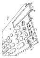
- Figure 1 is a perspective view of a key mat and keyboard PCB according to the invention.
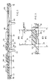
- Figure 2 is a section of the key mat on the line A-A of Figure 1; and
- Figure 3 is an enlarged fragmentary view of the key mat that is sectioned in the region of a single key.
- In Figure 1 a
printed circuit board 10 for a keypad according to the invention has on its top face an array of conductors includingrow conductors 11 andcolumn conductors 12 that define a matrix within which there arecontact areas 13 corresponding to eachkey 14 in anoverlying key mat 15. It will be noted that eachcontact area 13 comprises an interlaced array of conductive fingers (in this instance a 3 pronged fork entering a four pronged receptacle). The purpose of this interleaved array is to provide an area which is comparable to that of theoverlying key 14 within which contact may be made to signal that the key has been depressed. - The kay
mat 15 is a moulding in an elastomeric material such as silicon rubber or a rubber-modified polyurethane that when untensioned is of slightly lesser width and length than thecircuit board 10. It has an integrally mouldedperipheral lip 16 that has at its extremity a dependingrim 17. The lip can be engaged with the edges of theboard 10 to retain themat 15 in a predetermined location thereon with themat 15 in tension both longitudinally and transversely. The advantage of this arrangement is that moulding tolerances in themat 15 are substantially cancelled out when themat 15 is fitted to theboard 10 and eachkey 14 overlies therespective contact area 13 to a sufficient degree of accuracy to be serviceable. Furthermore therim 17 is stretched to accurate predetermined dimensions so that it will locate properly in a recess in a chassis member to which the keyboard is to be secured. The rigidity of theboard 10 should be such that the assembled keypad is self-supporting and does not require external reinforcement and thekeys 14 are maintained in stable positions without the need for an alignment bezel to be present as in conventional calculators and in membrane-type keyboards such as that of the Sinclar Spectrum. - Depending upon the overall dimensions of the keypad it may be desirable to provide location and retaining means at intermediate positions widthwise and lengthwise thereof. Accordingly the
board 10 is provided at appropriate positions with a pattern of location points in the form of through holes and thekey mat 15 has a complementary pattern of locating studs. Each stud comprises ashank 20 that fits into the respective through hole, a retaining head ormushroom 21 and a dependingfinger 22 by which thehead 21 can be pulled through the through hole. - The
board 10 andmat 15 may be apertured to accommodate awindow 23 for a display device such as a liquid crystal or LED display. Thewindow 23 preferably has arim 24 that engages in arecess 25 in themat 15 to maintain themat 15 flat on theboard 10 notwithstanding the tension therein. It hasfingers 26 that extend through the aperture inboard 10 andmat 15 and locate on the underside of theboard 10. It will be appreciated that in the present arrangement the exposed face of the keypad is a continuous sheet of elastomer interrupted only by the non-moving windows about which there is an effective seal so that the assembly is protected from the ingress of moisture and dirt. Between the keys the exposed face of the key mat is pulled smooth by the slight tension therein and the key mat should be at least 1.5 mm thick so that soldered component leads in the top face ofboard 10 or other protuberances can be concealed in recesses let into the lower face of themat 15, as can air channels (described below) between the keys. If the dimensions of thewindow 23 exceed the dimensions of the device to be displayed therein there may be an area 27 of themat 15 that is relieved to underlie thewindow 23 and may carry information in the form of raised lettering or printed areas that are formed at the time of moulding. Alternatively a pre-printed paper label can be retained in the relieved area. Furthermore thekeys 14 may have printed or moulded in legends and legends such as a manufacturer's logo may be moulded into blank areas of themat 15. It will be appreciated therefore that a key mat having a number of keys and the appropriate windows together with other indicia may be formed at a single mould operation. - As is apparent from, the foregoing the
keys 14 are depressed to operate them and have on their undersidesconductive pads 29 that when brought into contact with thecontact areas 13 make a circuit between at least one pair of the interlaced contact fingers, so that a state corresponding to the depressed key is caused to exist in the row andcolumn conductors conductive pad 29 e.g. of graphite filled rubber that is somewhat harder than elastomer of themat 15 is provided as a disc that is inserted into the mould for themat 15 and is moulded into the underside of eachkey 14. Eachkey 14 is preferably of circular or other non-angular shape, has substantially the thickness of themat 15 and stands slightly proud as shown. It is joined to the body of themat 15 by means of awall 30 of thinner material which when viewed in section is directed at approximately 45o to the body of themat 15. As thekey 14 is depressed thewall 30 exhibits an over-centre action such that depression of the key beyond its mid travel will with high probability result in thepad 29 contacting thearea 13. The thickness of thewall 30 is selected to give the desired tactile feedback to the keyboard operator, and the length thereof is selected in accordance with the intended travel of each key. The shape of thekey 14 andwall 30 is selected to avoid stress concentrations resulting in fatigue. The underside of thepad 29 is convex with a large radius of curvature that is also appropriate to the key travel and size so that it will touch thecontact area 13 tangentially (i.e. surface to surface and not edge to surface) irrespective of whether or not thekey 14 loses its proper attitude when it is depressed. Therefore the keyboard operator can strike the key off-centre and still make an effective contact, thesubstantial contact area 13 under theconductive pad 29 cooperating to achieve this result. Furthermore it has been found that the material of thekey 14 is less likely to intrude onto the working face of theconductive pad 29 during the moulding process if thepad 29 is convex as shown, so that the reject rate is reduced.Air grooves 31 let into the lower face of themat 15 interconnect theseveral keys 14 to permit the key travel to take place. - In Figure 3 the functional relationships between the various parts of an individual switch are apparent in a practical example. The
key mat 15 has a key-surrounding portion 2.25 mm thick in which are letair passages 31 that are 0.5 mm high. The key top diameter ⌀ A is in thisinstance 10 mm and it is tapered to a rim outside diameter ⌀ B of 11 mm. Thewall 30 is of length 1.4 mm so that the base diameter ⌀ C of the cavity underlying thekey 14 is 13 mm. The diameter ⌀ D of theconductive pad 29 under thekey 14 is given by:
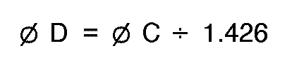
and in this instance is 9.1 mm, the relation between ⌀ D and ⌀ C having been empirically determined. The convex surface of thepad 29 has a radius of curvature ROC given by:

and in the example given is 34 mm. Thekey 14 and moulding are 3.24 mm deep and the overall key height E is given by:

and is 4.75 mm. The travel between theconductive pad 29 and the underlying conductor is about 1.5 mm. - It will be appreciated that the present construction is readily adaptable to making keyboards of a variety of shapes, key numbers and key positions, can incorporate keys of different tactility so that eg. the numeric keys are stiffer than the alphabetical keys.
- Various modifications may be made to the described embodiment without departing from the invention, the scope of which is defined in the appended claims. For example, the
board 10 could be replaced by a membrane switch over an underlying support of e.g. aluminium sheet. LED's could be provided in theboard 10 and amat 15 of transluscent material could be used, thereby providing the possibility of back-lighting thewall 30 around each key.
Claims (8)
- A keypad consisting of a combined cover and membrane or key mat (15) of resiliently deformable material and a contact surface or board (10) bearing open-circuit conductors (12, 13) against which board (10) the combined cover and key mat (15) is positioned with otherwise unsupported integral touch pads or keys (14) disposed in an array and each raised from the surrounding key mat (15) by an angled wall (30) arranged so that finger pressure on any key (14) depresses it until a conductive pad (29) forming the 0nderside of the key (14) contacts the board (10) and makes the circuit between the conductors (12, 13), each key (14) and the surrounding key mat (15) being relatively thick and the wall (30) being relatively thin, and the wall (30) being relatively short in comparison with the outer diameter (⌀B) across the associated key (14) characterised in that:(a) the wall (30) has only a small fraction of the thickness of the surrounding key mat (15) so that the wall (30) flexes under finger pressure on the key (14) without deflecting the surrounding key mat (15);(b) the keystroke is greater than the projection of the wall (30) along the keystroke direction so that the wall (30) gives way through an over-centre position to give a tactile sensation; and(c) each conductive pad (29) covers the whole lower face of the key (14) and has a continuous convex curvature (ROC) selected in relation to the length of the wall (30) and the outer diameter across the key (14), such that it contacts the board (10) tangentially when the key (14) is tilted by asymmetric finger pressure.
- A keypad according to claim 1, wherein the ratio of the width of the wall (30) to the outer diameter (⌀B) of the key (14) is about 0.1, the ratio of the diameter (⌀D) the conductive pad (29) to the outer diameter (⌀B) of the key (14) is about 0.8, the radius of curvature (ROC) of the convex conductive pad (29) is about 2.6 ⌀C where ⌀C is the base diameter of the cavity underlying the key (14) or the distance between the locations where opposed parts of the wall (30) join the key mat (15) and the conductive pad (29) is a moulded-in conductive pad of elastomer that is a harder material than the material of the membrane (15) and key (14).
- A keypad according to any preceding claim, wherein the key mat (15) is moulded slighly under the size of the board (10) and has a peripheral lip (16) into which edges of the board (10) locate to maintain the key mat (15) in position against the board (10) and to tension the key mat (15).
- A keypad according to claim 3, wherein retaining studs (20, 21) project from the underside of the key mat (15) and locate in through holes in the board (10).
- A keypad according to any preceding claim, wherein the board (10) is a printed circuit board formed with an array of interdigitated contacts under each key (14).
- A keypad according to any preceding claim, wherein the visible face of each key (14) is individually coloured or marked for identification.
- A keypad according to any preceding claim, wherein the key mat (15) is of transluscent material and a light source or light sources back-light at least one of keys (14).
- A keypad as claimed in any preceding claim, wherein the key mat (15) and key (14) are of substantially the same thickness and the pad (29) is disposed no higher than the line of the top surface of the key mat (15).
Priority Applications (1)
| Application Number | Priority Date | Filing Date | Title |
|---|---|---|---|
| AT85900720T ATE79197T1 (en) | 1984-02-03 | 1985-02-04 | IMPROVEMENTS IN SWITCHES AND KEYBOARDS. |
Applications Claiming Priority (2)
| Application Number | Priority Date | Filing Date | Title |
|---|---|---|---|
| GB848402974A GB8402974D0 (en) | 1984-02-03 | 1984-02-03 | Switches and keyboards |
| GB8402974 | 1984-02-03 |
Publications (2)
| Publication Number | Publication Date |
|---|---|
| EP0203068A1 EP0203068A1 (en) | 1986-12-03 |
| EP0203068B1 true EP0203068B1 (en) | 1992-08-05 |
Family
ID=10556075
Family Applications (1)
| Application Number | Title | Priority Date | Filing Date |
|---|---|---|---|
| EP85900720A Expired EP0203068B1 (en) | 1984-02-03 | 1985-02-04 | Improvements in switches and keyboards |
Country Status (7)
| Country | Link |
|---|---|
| US (2) | US4634818A (en) |
| EP (1) | EP0203068B1 (en) |
| AT (1) | ATE79197T1 (en) |
| AU (1) | AU584606B2 (en) |
| DE (1) | DE3586460T2 (en) |
| GB (1) | GB8402974D0 (en) |
| WO (1) | WO1985003595A1 (en) |
Cited By (1)
| Publication number | Priority date | Publication date | Assignee | Title |
|---|---|---|---|---|
| DE102007035923A1 (en) * | 2007-07-23 | 2009-02-05 | Silcos Gmbh | Operating device for electrical switching operation in medical field, has readjusting unit, operating unit and actuating unit formed as integrated unit, where operating surface of device is closed |
Families Citing this family (78)
| Publication number | Priority date | Publication date | Assignee | Title |
|---|---|---|---|---|
| GB8402974D0 (en) * | 1984-02-03 | 1984-03-07 | Npm Int | Switches and keyboards |
| AU598813B2 (en) * | 1986-05-20 | 1990-07-05 | Exicom Australia Pty Limited | Membrane keyboard |
| US4818829A (en) * | 1987-07-09 | 1989-04-04 | Duralith Corporation | Integrally molded composites of silicone rubber |
| US5087798A (en) * | 1990-03-14 | 1992-02-11 | Rodgers Instrument Corporation | Illuminated elastomeric rocker switch assembly |
| US5187336A (en) * | 1990-05-30 | 1993-02-16 | The Cherry Corporation | Switch assembly with transfer actuator |
| US5311656A (en) * | 1991-03-12 | 1994-05-17 | Mitel Corporation | Keypad method of manufacture |
| DE4112754C2 (en) * | 1991-04-19 | 1999-06-02 | Marquardt Gmbh | Push button switch |
| GB2266186B (en) * | 1992-04-14 | 1995-09-20 | Motorola Gmbh | A keyboard |
| US5358344A (en) * | 1992-09-01 | 1994-10-25 | Key Tronic Corporation | Keyboard with full-travel, self-leveling keyswitches |
| US5422447A (en) * | 1992-09-01 | 1995-06-06 | Key Tronic Corporation | Keyboard with full-travel, self-leveling keyswitches and return mechanism keyswitch |
| US5475192A (en) * | 1993-03-15 | 1995-12-12 | Teikoku Tsushin Kogyo Co., Ltd. | Keytop sheet for push-button switches |
| US5973621A (en) * | 1993-06-03 | 1999-10-26 | Levy; David | Compact keyed input device |
| US5399821A (en) * | 1993-10-20 | 1995-03-21 | Teikoku Tsushin Kogyo Co., Ltd. | Keytop for push-button switches, and method of manufacturing same |
| AU8138794A (en) * | 1993-10-26 | 1995-05-22 | Marketing Partners, Gesellschaft fur Marketing-Projecting und Marketing-Services mbH | Flat input keyboard for data processing machines or the like and process for producing the same |
| US5557299A (en) * | 1994-05-04 | 1996-09-17 | Kidtech, Inc. | Method and apparatus for a learning styled computer keyboard |
| EP0685860A1 (en) * | 1994-06-03 | 1995-12-06 | Hewlett-Packard Company | Full travel, sealed, fully backlighted keyboard |
| DE9412474U1 (en) * | 1994-08-03 | 1994-12-08 | AutoAir Klimaanlagen GmbH, 47574 Goch | Air conditioning switch unit |
| FI106826B (en) * | 1994-09-16 | 2001-04-12 | Nokia Mobile Phones Ltd | installing Carpet |
| US5521342A (en) * | 1994-12-27 | 1996-05-28 | General Motors Corporation | Switch having combined light pipe and printed circuit board |
| FR2750229A1 (en) * | 1996-06-19 | 1997-12-26 | Philips Electronics Nv | KEY DEVICE HAVING A CURVED KEYBOARD |
| US5739486A (en) * | 1996-08-07 | 1998-04-14 | Ford Motor Company | Push-button system for control panels |
| JPH10116639A (en) * | 1996-10-15 | 1998-05-06 | Shin Etsu Polymer Co Ltd | Thin type push-button switch member |
| TW358571U (en) * | 1997-10-24 | 1999-05-11 | Acer Peripherals Inc | Water proofing keyboard |
| AU1397099A (en) * | 1997-11-12 | 1999-05-31 | Think Outside | System and method for detecting key actuation in a keyboard |
| JP3134989B2 (en) * | 1998-02-06 | 2001-02-13 | 日本電気株式会社 | Electronic device mounting structure |
| JPH11238423A (en) * | 1998-02-20 | 1999-08-31 | Porimatec Kk | Contact key switch and its manufacture |
| GB2336457A (en) * | 1998-04-14 | 1999-10-20 | Ford Motor Co | Button carrier and display backlight |
| US5967297A (en) * | 1998-07-17 | 1999-10-19 | Methode Electronics, Inc. | Wiping elastomeric switch |
| EP1003188A3 (en) * | 1998-11-19 | 2001-04-25 | Key Tronic Corporation | Ergonomic computer keyboard |
| DE29821579U1 (en) * | 1998-12-02 | 1999-05-27 | Detewe-Deutsche Telephonwerke Ag & Co, 10997 Berlin | One-piece keyboard |
| FI105504B (en) * | 1998-12-28 | 2000-08-31 | Nokia Mobile Phones Ltd | New push button design for user interface of electronic device |
| GB9930170D0 (en) * | 1999-12-21 | 2000-02-09 | Spring Trading Ltd | Communication devices |
| DE60108868T2 (en) * | 2000-05-22 | 2006-03-23 | Digit Wireless, LLC, Cambridge | INPUT DEVICES AND THEIR USE |
| JP4414066B2 (en) * | 2000-06-15 | 2010-02-10 | ポリマテック株式会社 | Laminated key sheet |
| FI108682B (en) | 2000-06-30 | 2002-02-28 | Nokia Corp | Method for manufacturing the keyboard of an electronic device |
| FI110044B (en) | 2000-06-30 | 2002-11-15 | Nokia Corp | Structure of the casing part of an electronic device |
| DE20014172U1 (en) | 2000-08-17 | 2000-12-07 | Schurter GmbH, 79346 Endingen | Keyboard for triggering electrical switching functions |
| DE10062380A1 (en) * | 2000-12-14 | 2002-07-04 | Siemens Ag | Keyboard assembly for an electronic device and electronic device |
| US6750414B2 (en) * | 2001-06-18 | 2004-06-15 | Marking Specialists/Polymer Technologies, Inc. | Tactile keyboard for electrical appliances and equipment |
| US20080230282A1 (en) * | 2005-08-05 | 2008-09-25 | Weightech, Inc. | Modular sealed portable digital electronic controller |
| US7126498B2 (en) * | 2002-02-27 | 2006-10-24 | Digit Wireless, Llc | Keypad construction |
| CN1307672C (en) * | 2002-05-23 | 2007-03-28 | 数字无线有限责任公司 | keypad |
| DE20212255U1 (en) * | 2002-08-08 | 2002-12-19 | TRW Automotive Electronics & Components GmbH & Co. KG, 78315 Radolfzell | The multifunctional pushbutton switch |
| US6850418B2 (en) * | 2002-09-19 | 2005-02-01 | Timekeeping Systems, Inc. | Impact resistant electronic data module housing |
| US20040089705A1 (en) * | 2002-11-13 | 2004-05-13 | Yuan Chien Shen | Waterproof mechanism of key of handheld computer |
| DE10310035A1 (en) * | 2003-03-06 | 2004-09-16 | Burg-Wächter Kg | Device comprising a carrier element with preferably up to 12 keys and/or pressure elements useful for introduction and optical representation of control commands in electronic data processing devices for control of alarm equipment |
| DE10310230B4 (en) * | 2003-03-06 | 2005-12-01 | Burg-Wächter Kg | Device for inputting and visualizing control commands in electronic data processing devices |
| FR2854726B1 (en) * | 2003-05-09 | 2005-08-26 | St Microelectronics Sa | MICROCOMMUTER WITH SEVERAL CLOSED POSITIONS WITH SIDE MOVEMENT |
| JP2005063945A (en) * | 2003-07-30 | 2005-03-10 | Tokai Rika Co Ltd | Contact structure of switch, and method for manufacturing switch contact |
| US7844309B2 (en) * | 2004-02-27 | 2010-11-30 | Nokia Corporation | Exchangeable keymat |
| US20070130078A1 (en) * | 2005-12-02 | 2007-06-07 | Robert Grzesek | Digital rights management compliance with portable digital media device |
| US7394030B2 (en) | 2005-06-02 | 2008-07-01 | Palm, Inc. | Small form-factor keyboard using keys with offset peaks and pitch variations |
| US7022929B1 (en) * | 2005-07-20 | 2006-04-04 | Delphi Technologies, Inc. | Detectable push-pull-though details for switch pad |
| US7657994B2 (en) * | 2005-10-19 | 2010-02-09 | Delphi Technologies, Inc. | Method for installing a switch pad |
| US7832628B2 (en) * | 2005-10-21 | 2010-11-16 | Verifone, Inc. | Protective cover for terminal keypad security switches |
| GB2435448B (en) * | 2006-02-20 | 2009-12-02 | Devlin Electronics Ltd | A Healthcare keyboard |
| DE202006004575U1 (en) * | 2006-03-22 | 2006-05-18 | Trw Automotive Electronics & Components Gmbh & Co. Kg | switch module |
| US8089776B2 (en) * | 2006-06-19 | 2012-01-03 | Sony Ericsson Mobile Communications Ab | Side switch for a contact exposed on an edge of a circuit board and method |
| US7259339B1 (en) * | 2006-09-08 | 2007-08-21 | Palm, Inc. | Enhanced key structure with combined keycap for a mobile computing device |
| US8989822B2 (en) | 2006-09-08 | 2015-03-24 | Qualcomm Incorporated | Keypad assembly for use on a contoured surface of a mobile computing device |
| US20090262492A1 (en) * | 2007-10-26 | 2009-10-22 | Seal Shield, Llc | Submersible keyboard |
| TWI396114B (en) * | 2009-04-10 | 2013-05-11 | Askey Computer Corp | A modularized keyboard and its manufacturing method |
| US8232485B2 (en) | 2009-09-28 | 2012-07-31 | Research In Motion Limited | Key assembly for an electronic device having a multi-character keycap |
| US8362371B2 (en) * | 2009-09-28 | 2013-01-29 | Research In Motion Limited | Key assembly for an electronic device having one-piece keycaps and multi-touch preventing supports |
| US8283582B2 (en) * | 2010-06-30 | 2012-10-09 | Research In Motion Limited | Deflection web for a keypad assembly |
| US8647203B2 (en) * | 2011-11-04 | 2014-02-11 | Target Brands, Inc. | Transaction product with selectively illuminated buttons |
| US8622246B2 (en) | 2012-02-13 | 2014-01-07 | Ecolab Usa Inc. | Fluid reservoir docking station |
| US9449769B2 (en) * | 2012-10-30 | 2016-09-20 | Apple Inc. | Low travel dome and systems for using the same |
| TWI550978B (en) * | 2014-02-25 | 2016-09-21 | 達方電子股份有限公司 | Positioning mechanism, positioning unit and method thereof and keyboard having the same |
| US12366085B2 (en) | 2015-08-06 | 2025-07-22 | Luciana E. Hanley | Hovering air fort |
| US10083807B2 (en) | 2016-05-24 | 2018-09-25 | Apple Inc. | Metal switch for input device |
| USD896809S1 (en) * | 2018-02-28 | 2020-09-22 | Shenzhen Hastech Industries Co., Ltd. | Bluetooth keyboard |
| DE102018108660B3 (en) * | 2018-04-12 | 2019-10-17 | Preh Gmbh | Switch arrangement with switching mat for operating a motor vehicle component |
| USD908697S1 (en) * | 2018-06-04 | 2021-01-26 | Logitech Europe S.A. | Keyboard |
| USD902928S1 (en) * | 2018-07-12 | 2020-11-24 | Shenzhen Hastech Industries Co., Ltd. | Bluetooth keyboard |
| USD961592S1 (en) * | 2020-12-31 | 2022-08-23 | Shenzhen Mofei Electronics Co., Limited | Keyboard |
| US20230243186A1 (en) * | 2022-01-31 | 2023-08-03 | Lewis Hyman, Inc. | Electronic door lock with keypad |
| TWI801252B (en) * | 2022-05-30 | 2023-05-01 | 融程電訊股份有限公司 | Button structure of radio intercom with buttons of different colors and manufacturing method thereof |
Family Cites Families (18)
| Publication number | Priority date | Publication date | Assignee | Title |
|---|---|---|---|---|
| FR871287A (en) * | 1940-04-29 | 1942-04-17 | Licentia Gmbh | Watertight protection device for electric control buttons |
| US3054879A (en) * | 1960-01-20 | 1962-09-18 | Indak Mfg Corp | Pushbutton switch |
| US3728509A (en) * | 1970-09-26 | 1973-04-17 | Alps Electric Co Ltd | Push-button switch with resilient conductive contact member with downwardly projecting ridges |
| US3760137A (en) * | 1970-10-05 | 1973-09-18 | Alps Electric Co Ltd | Matrix push-button switch |
| US3761944A (en) * | 1971-01-22 | 1973-09-25 | Alps Electric Co Ltd | Binary code generator |
| US3699294A (en) * | 1971-05-18 | 1972-10-17 | Flex Key Corp | Keyboard, digital coding, switch for digital logic, and low power detector switches |
| US3932722A (en) * | 1974-04-16 | 1976-01-13 | Nippo Communication Industrial Co., Ltd. | Push button body for a push-button switch providing snap-action of the switch |
| DE2540011C3 (en) * | 1974-09-09 | 1979-08-23 | Sharp K.K., Osaka (Japan) | Electronic calculator |
| US4081631A (en) * | 1976-12-08 | 1978-03-28 | Motorola, Inc. | Dual purpose, weather resistant data terminal keyboard assembly including audio porting |
| US4127758A (en) * | 1977-10-13 | 1978-11-28 | Sheldahl, Inc. | Tactile layer having hinged dome |
| JPS5686723U (en) * | 1979-12-07 | 1981-07-11 | ||
| DE3032557C2 (en) * | 1980-08-29 | 1985-02-07 | Standard Elektrik Lorenz Ag, 7000 Stuttgart | Rubber elastic tactile contact element |
| JPS58117619A (en) * | 1981-12-29 | 1983-07-13 | キヤノン株式会社 | Electronic equipment |
| JPS58115027U (en) * | 1982-02-01 | 1983-08-05 | サンアロ−株式会社 | push button panel |
| DE3218404A1 (en) * | 1982-05-15 | 1983-11-17 | Wolfgang Schulte | Keypad for a printed circuit |
| US4421966A (en) * | 1982-07-26 | 1983-12-20 | Kb Denver, Inc. | Keyboard elastomeric cover with buttons having changeable legends |
| DE3481670D1 (en) * | 1983-04-20 | 1990-04-19 | Bebie & Co | KEYBOARD ARRANGEMENT. |
| GB8402974D0 (en) * | 1984-02-03 | 1984-03-07 | Npm Int | Switches and keyboards |
-
1984
- 1984-02-03 GB GB848402974A patent/GB8402974D0/en active Pending
-
1985
- 1985-02-04 DE DE8585900720T patent/DE3586460T2/en not_active Expired - Fee Related
- 1985-02-04 AU AU39339/85A patent/AU584606B2/en not_active Ceased
- 1985-02-04 WO PCT/GB1985/000049 patent/WO1985003595A1/en not_active Ceased
- 1985-02-04 EP EP85900720A patent/EP0203068B1/en not_active Expired
- 1985-02-04 US US06/783,927 patent/US4634818A/en not_active Expired - Fee Related
- 1985-02-04 AT AT85900720T patent/ATE79197T1/en not_active IP Right Cessation
-
1987
- 1987-12-10 US US07/131,630 patent/US4839474A/en not_active Expired - Lifetime
Cited By (2)
| Publication number | Priority date | Publication date | Assignee | Title |
|---|---|---|---|---|
| DE102007035923A1 (en) * | 2007-07-23 | 2009-02-05 | Silcos Gmbh | Operating device for electrical switching operation in medical field, has readjusting unit, operating unit and actuating unit formed as integrated unit, where operating surface of device is closed |
| DE102007035923B4 (en) * | 2007-07-23 | 2011-12-29 | Silcos Gmbh | operating element |
Also Published As
| Publication number | Publication date |
|---|---|
| US4839474A (en) | 1989-06-13 |
| US4634818A (en) | 1987-01-06 |
| ATE79197T1 (en) | 1992-08-15 |
| AU584606B2 (en) | 1989-06-01 |
| WO1985003595A1 (en) | 1985-08-15 |
| EP0203068A1 (en) | 1986-12-03 |
| DE3586460T2 (en) | 1993-03-04 |
| GB8402974D0 (en) | 1984-03-07 |
| AU3933985A (en) | 1985-08-27 |
| DE3586460D1 (en) | 1992-09-10 |
Similar Documents
| Publication | Publication Date | Title |
|---|---|---|
| AU584606B2 (en) | Switches and keyboards | |
| US5329079A (en) | Computer keyboard with improved cantilever switch design | |
| US4430531A (en) | Snap disc keyboard | |
| US5136131A (en) | Push-button switch including a sheet provided with a plurality of domed members | |
| US5015829A (en) | Key pad and front panel assembly for an electronic instrument | |
| US5481074A (en) | Computer keyboard with cantilever switch and actuator design | |
| US4338502A (en) | Metallic housing for an electronic apparatus with a flat keyboard | |
| US4314116A (en) | Keyboard switch with graphic overlay | |
| US4421966A (en) | Keyboard elastomeric cover with buttons having changeable legends | |
| US4160886A (en) | Keyboards and methods of making keyboards | |
| US4640994A (en) | Electronic apparatus with a flat panel keyboard unit | |
| US5777281A (en) | Key assembly | |
| US4228330A (en) | Touch panel mechanism | |
| US5926119A (en) | Numeric keypad configuration | |
| JPH1031929A (en) | Key pad structure | |
| EP0232137A2 (en) | Improvements in or relating to relegendable pushbutton switches | |
| US4194099A (en) | Control panel overlay | |
| US4085306A (en) | Keyboard switch assemblies | |
| EP1540684B1 (en) | Keyboard improvements | |
| US4375585A (en) | Deformable switch keyboard | |
| US20040238340A1 (en) | Switch arrangement | |
| GB2181283A (en) | Electronically reconfigurable keyboard | |
| JPH0475219A (en) | character input device | |
| JPH039488B2 (en) | ||
| JPH08273477A (en) | Push button apparatus |
Legal Events
| Date | Code | Title | Description |
|---|---|---|---|
| PUAI | Public reference made under article 153(3) epc to a published international application that has entered the european phase |
Free format text: ORIGINAL CODE: 0009012 |
|
| 17P | Request for examination filed |
Effective date: 19860724 |
|
| AK | Designated contracting states |
Kind code of ref document: A1 Designated state(s): AT BE CH DE FR GB LI NL SE |
|
| 17Q | First examination report despatched |
Effective date: 19880310 |
|
| RAP1 | Party data changed (applicant data changed or rights of an application transferred) |
Owner name: KEYMAT TECHNOLOGY LIMITED |
|
| GRAA | (expected) grant |
Free format text: ORIGINAL CODE: 0009210 |
|
| AK | Designated contracting states |
Kind code of ref document: B1 Designated state(s): AT BE CH DE FR GB LI NL SE |
|
| PG25 | Lapsed in a contracting state [announced via postgrant information from national office to epo] |
Ref country code: SE Free format text: THE PATENT HAS BEEN ANNULLED BY A DECISION OF A NATIONAL AUTHORITY Effective date: 19920805 Ref country code: NL Effective date: 19920805 Ref country code: LI Effective date: 19920805 Ref country code: CH Effective date: 19920805 Ref country code: BE Effective date: 19920805 Ref country code: AT Effective date: 19920805 |
|
| REF | Corresponds to: |
Ref document number: 79197 Country of ref document: AT Date of ref document: 19920815 Kind code of ref document: T |
|
| REF | Corresponds to: |
Ref document number: 3586460 Country of ref document: DE Date of ref document: 19920910 |
|
| REG | Reference to a national code |
Ref country code: CH Ref legal event code: PL |
|
| ET | Fr: translation filed | ||
| NLV1 | Nl: lapsed or annulled due to failure to fulfill the requirements of art. 29p and 29m of the patents act | ||
| PLBE | No opposition filed within time limit |
Free format text: ORIGINAL CODE: 0009261 |
|
| STAA | Information on the status of an ep patent application or granted ep patent |
Free format text: STATUS: NO OPPOSITION FILED WITHIN TIME LIMIT |
|
| 26N | No opposition filed | ||
| REG | Reference to a national code |
Ref country code: GB Ref legal event code: IF02 |
|
| PGFP | Annual fee paid to national office [announced via postgrant information from national office to epo] |
Ref country code: FR Payment date: 20020212 Year of fee payment: 18 |
|
| PGFP | Annual fee paid to national office [announced via postgrant information from national office to epo] |
Ref country code: DE Payment date: 20020227 Year of fee payment: 18 |
|
| PG25 | Lapsed in a contracting state [announced via postgrant information from national office to epo] |
Ref country code: DE Free format text: LAPSE BECAUSE OF NON-PAYMENT OF DUE FEES Effective date: 20030902 |
|
| PG25 | Lapsed in a contracting state [announced via postgrant information from national office to epo] |
Ref country code: FR Free format text: LAPSE BECAUSE OF NON-PAYMENT OF DUE FEES Effective date: 20031031 |
|
| REG | Reference to a national code |
Ref country code: FR Ref legal event code: ST |
|
| PGFP | Annual fee paid to national office [announced via postgrant information from national office to epo] |
Ref country code: GB Payment date: 20040218 Year of fee payment: 20 |
|
| PG25 | Lapsed in a contracting state [announced via postgrant information from national office to epo] |
Ref country code: GB Free format text: LAPSE BECAUSE OF EXPIRATION OF PROTECTION Effective date: 20050203 |
|
| REG | Reference to a national code |
Ref country code: GB Ref legal event code: PE20 |