EP0199332A1 - Empfänger für optische Breitbandsignale - Google Patents
Empfänger für optische Breitbandsignale Download PDFInfo
- Publication number
- EP0199332A1 EP0199332A1 EP86105515A EP86105515A EP0199332A1 EP 0199332 A1 EP0199332 A1 EP 0199332A1 EP 86105515 A EP86105515 A EP 86105515A EP 86105515 A EP86105515 A EP 86105515A EP 0199332 A1 EP0199332 A1 EP 0199332A1
- Authority
- EP
- European Patent Office
- Prior art keywords
- unit
- transistor
- receiver according
- amplifier
- pole
- Prior art date
- Legal status (The legal status is an assumption and is not a legal conclusion. Google has not performed a legal analysis and makes no representation as to the accuracy of the status listed.)
- Granted
Links
- 230000003287 optical effect Effects 0.000 title claims abstract description 16
- 230000003321 amplification Effects 0.000 claims abstract description 7
- 238000003199 nucleic acid amplification method Methods 0.000 claims abstract description 7
- 230000003071 parasitic effect Effects 0.000 claims description 5
- 230000006978 adaptation Effects 0.000 claims description 3
- 230000001131 transforming effect Effects 0.000 claims description 3
- 230000000750 progressive effect Effects 0.000 claims 2
- 235000021183 entrée Nutrition 0.000 description 12
- 239000003990 capacitor Substances 0.000 description 8
- 244000045947 parasite Species 0.000 description 5
- 238000002513 implantation Methods 0.000 description 4
- 238000004519 manufacturing process Methods 0.000 description 3
- 230000010287 polarization Effects 0.000 description 3
- 239000000758 substrate Substances 0.000 description 3
- 241001080024 Telles Species 0.000 description 2
- 230000010354 integration Effects 0.000 description 2
- JBRZTFJDHDCESZ-UHFFFAOYSA-N AsGa Chemical compound [As]#[Ga] JBRZTFJDHDCESZ-UHFFFAOYSA-N 0.000 description 1
- GYHNNYVSQQEPJS-UHFFFAOYSA-N Gallium Chemical compound [Ga] GYHNNYVSQQEPJS-UHFFFAOYSA-N 0.000 description 1
- 229910001218 Gallium arsenide Inorganic materials 0.000 description 1
- 241000287107 Passer Species 0.000 description 1
- 240000008042 Zea mays Species 0.000 description 1
- 230000001154 acute effect Effects 0.000 description 1
- PNEYBMLMFCGWSK-UHFFFAOYSA-N aluminium oxide Inorganic materials [O-2].[O-2].[O-2].[Al+3].[Al+3] PNEYBMLMFCGWSK-UHFFFAOYSA-N 0.000 description 1
- 230000003416 augmentation Effects 0.000 description 1
- 239000000470 constituent Substances 0.000 description 1
- 238000010586 diagram Methods 0.000 description 1
- 230000000694 effects Effects 0.000 description 1
- 229910052733 gallium Inorganic materials 0.000 description 1
- 229910052751 metal Inorganic materials 0.000 description 1
- 239000002184 metal Substances 0.000 description 1
- 238000005498 polishing Methods 0.000 description 1
- 230000000135 prohibitive effect Effects 0.000 description 1
- 230000001105 regulatory effect Effects 0.000 description 1
- 229920006395 saturated elastomer Polymers 0.000 description 1
- 230000009466 transformation Effects 0.000 description 1
Images

Classifications
-
- H—ELECTRICITY
- H04—ELECTRIC COMMUNICATION TECHNIQUE
- H04B—TRANSMISSION
- H04B10/00—Transmission systems employing electromagnetic waves other than radio-waves, e.g. infrared, visible or ultraviolet light, or employing corpuscular radiation, e.g. quantum communication
- H04B10/60—Receivers
- H04B10/66—Non-coherent receivers, e.g. using direct detection
- H04B10/69—Electrical arrangements in the receiver
- H04B10/693—Arrangements for optimizing the preamplifier in the receiver
- H04B10/6932—Bandwidth control of bit rate adaptation
Definitions
- the present invention relates to a circuit for receiving optical signals, said receiver being intended to operate with a very wide bandwidth, which can range from a few kilohertz at 3dB to approximately 1 Gigahertz at 3dB, and even beyond.
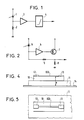
- an optical receiver for example an avalanche photodiode or PIN, associated with a load resistor 2, and an electronic amplifier 3.
- the resistor 2 to obtain an acceptable signal-to-noise ratio, must have a high value , so that it necessarily creates, with the input capacity of amplifier 3, a low-pass filter cut-off pole. It is then conventional to compensate this pole by an equalizer stage 4, making it possible to reject this pole above the frequency band to be transmitted, conventionally constituted by a transistor mounted as a common emitter.
- Such a device is not adaptable to very wide band optical receivers, because it would require too many cascade equalizer stages for the device to operate at frequencies reaching or exceeding one Gigahertz. Furthermore, a device comprising several cascaded equalizers is very difficult to adjust, since an equalizer cannot be adjusted without retouching the one above, which makes it unsuitable for mass production. Finally, such a device, if it has to operate at high frequencies, cannot transmit the low-frequency service channels, since it then becomes saturated at low-frequency. Finally, such a device is very sensitive to temperature, since it does not have any regulatory element in the matter.
- a second known type of optical receiver structure is as shown - schematically in Figure 2 attached.
- a receiver of this type is for example sold by the American firm LASERTRON under the name "PINFET RECEIVER MODULE". It comprises, as shown, a photodiode 5, such as a PIN diode, an amplifier 6 comprising for example an FET transistor followed by a transistor forming with the first a stage of cascode type, an output stage of impedance adapter comprising a transistor 7 mounted as a common collector on an output resistor 8, and finally and above all a feedback resistor 9 mounted between the output of transistor 7 and the input of amplifier 6.
- a photodiode 5 such as a PIN diode
- an amplifier 6 comprising for example an FET transistor followed by a transistor forming with the first a stage of cascode type
- an output stage of impedance adapter comprising a transistor 7 mounted as a common collector on an output resistor 8
- finally and above all a feedback resistor 9 mounted between the output of transistor
- Such a transimpedance circuit operates satisfactorily up to frequencies which can range up to several hundred megahertz. It operates, up to these frequencies, with no added equalization stage, and does not present problems of saturation at low frequency and temperature resistance.
- said multi-stage and very broadband amplifier comprises at least a first amplification unit with two transistors, of the "common-collector and common-base, or" paraphase "type, and said pass-filter connection. high is placed between the first and the second transistor stage of said first unit
- said first paraphase unit is followed by a second paraphase unit of the same type.
- the feedback resistance R26 is constructed and installed so as to present the lowest possible parasitic capacity, it being understood that on the other hand the entire circuit of the FIG. 3 is produced as a function of the very high frequency to be passed, for example by microassembly and use of hybrid elements, which does not pose serious problems for those skilled in the art.
- FIGS 4 and 5 schematically represent an embodiment and possible implementation of the feedback resistance R26 of the invention.
- resistor R26 is terminated by two large connection terminals 12 and 13.
Landscapes
- Physics & Mathematics (AREA)
- Electromagnetism (AREA)
- Engineering & Computer Science (AREA)
- Computer Networks & Wireless Communication (AREA)
- Signal Processing (AREA)
- Amplifiers (AREA)
Applications Claiming Priority (2)
| Application Number | Priority Date | Filing Date | Title |
|---|---|---|---|
| FR8506332 | 1985-04-25 | ||
| FR8506332A FR2581275B1 (fr) | 1985-04-25 | 1985-04-25 | Recepteur de signaux optiques a tres large bande. |
Publications (2)
| Publication Number | Publication Date |
|---|---|
| EP0199332A1 true EP0199332A1 (de) | 1986-10-29 |
| EP0199332B1 EP0199332B1 (de) | 1990-10-24 |
Family
ID=9318685
Family Applications (1)
| Application Number | Title | Priority Date | Filing Date |
|---|---|---|---|
| EP86105515A Expired - Lifetime EP0199332B1 (de) | 1985-04-25 | 1986-04-22 | Empfänger für optische Breitbandsignale |
Country Status (4)
| Country | Link |
|---|---|
| US (1) | US4723313A (de) |
| EP (1) | EP0199332B1 (de) |
| DE (1) | DE3675065D1 (de) |
| FR (1) | FR2581275B1 (de) |
Families Citing this family (9)
| Publication number | Priority date | Publication date | Assignee | Title |
|---|---|---|---|---|
| NL8602408A (nl) * | 1986-09-24 | 1988-04-18 | Philips Nv | Voorversterker voor een optische ontvanger. |
| US5142401A (en) * | 1990-06-28 | 1992-08-25 | Raynet Corporation | Apparatus and method for a linear, wideband sensitive optical receiver |
| US5311353A (en) * | 1993-03-05 | 1994-05-10 | Analog Modules | Wide dynamic range optical receivers |
| US6303922B1 (en) * | 1997-07-21 | 2001-10-16 | Ortel Corporation | Range-switching optical receiver with high sensitivity and wide dynamic range |
| FR2783373B1 (fr) * | 1998-09-11 | 2002-10-31 | Dassault Electronique | Dispositif d'interface entre un capteur optoelectronique hyperfrequence a large bande et une charge |
| US20060115280A1 (en) * | 2004-11-30 | 2006-06-01 | Chang Jae J | Optical link bandwidth improvement |
| US20070152136A1 (en) * | 2006-01-04 | 2007-07-05 | Jianquo Yao | Transimpedance amplifier protection circuits |
| GB2434048A (en) * | 2006-01-16 | 2007-07-11 | Bookham Technology Plc | A protection circuit for a transimpedance amplifier with an APD input |
| US20150132008A1 (en) * | 2013-11-11 | 2015-05-14 | Taiwan Semiconductor Manufacturing Company, Ltd. | Via-less multi-layer integrated circuit with inter-layer interconnection |
Family Cites Families (2)
| Publication number | Priority date | Publication date | Assignee | Title |
|---|---|---|---|---|
| US2885495A (en) * | 1954-03-24 | 1959-05-05 | Rca Corp | Emitter coupled transistor amplifier |
| GB2140643B (en) * | 1983-05-19 | 1986-09-24 | Standard Telephones Cables Ltd | Optical fibre system |
-
1985
- 1985-04-25 FR FR8506332A patent/FR2581275B1/fr not_active Expired
-
1986
- 1986-04-22 DE DE8686105515T patent/DE3675065D1/de not_active Expired - Fee Related
- 1986-04-22 EP EP86105515A patent/EP0199332B1/de not_active Expired - Lifetime
- 1986-04-24 US US06/855,257 patent/US4723313A/en not_active Expired - Fee Related
Non-Patent Citations (4)
| Title |
|---|
| 6th ECOC, PROCEEDINGS OF THE SIXTH EUROPEAN CONFERENCE ON OPTICAL COMMUNICATION, York, 16-19 septembre 1980, pages 222-225; IEEE, Londres, GB; R.C. HOOPER et al.: "PIN-FET hybrid optical receivers for longer wavelength optical communications systems" * |
| ELECTRONICS LETTERS, vol. 19, no. 12, juin 1983, pages 445-447, Londres, GB; A.F. MITCHELL et al.: "PIN-bipolar optical receiver using a high-frequency high-beta transistor" * |
| IEEE JOURNAL OF SOLID-STATE CIRCUITS, vol. SC-19, no. 1, février 1984, pages 155-157, IEEE, New York, US; A. ARBEL et al.: "Regular correspondence. Low-noise high-speed optical receiver for fiber optic systems" * |
| IEEE TRANSACTIONS ON NUCLEAR SCIENCE; vol. NS-19, no. 1, février 1972, pages 388-395, New York, US; J.K. MILLARD et al.: "A broadband current preamplifier configuration for obtaining high resolution energy and time information from nuclear radiation detectors" * |
Also Published As
| Publication number | Publication date |
|---|---|
| US4723313A (en) | 1988-02-02 |
| EP0199332B1 (de) | 1990-10-24 |
| DE3675065D1 (de) | 1990-11-29 |
| FR2581275A1 (fr) | 1986-10-31 |
| FR2581275B1 (fr) | 1987-07-10 |
Similar Documents
| Publication | Publication Date | Title |
|---|---|---|
| CA2103859C (fr) | Source optique semiconductrice a predistorsion | |
| EP0016705B1 (de) | R.F.Stufe mit automatischer Verstärkungsregelung und Empfänger mit einer solchen Stufe | |
| EP0660512B1 (de) | Phasenschiebverstärker und seine Verwendung in einer Zusammenführungsschaltung | |
| EP0199332B1 (de) | Empfänger für optische Breitbandsignale | |
| FR2829316A1 (fr) | Attenuateur commande | |
| FR2719159A1 (fr) | Dispositif optoélectronique intégrant un photodétecteur à deux diodes. | |
| EP0130260A1 (de) | Schnittstellenmodul für Fernsprechleitungen | |
| EP0455570B1 (de) | Sehr breitbandige Verstärkungseinrichtung für Gleichstrom bis Mikrowellen, insbesondere geeignet für integrierte Schaltungen | |
| FR2460576A1 (fr) | Circuit d'alimentation a trois bornes pour appareil telephonique | |
| FR2549314A1 (fr) | Quadrupole d'adaptation, independante de la frequence de fonctionnement, d'une reactance, et amplificateur a ondes progressives utilisant un tel quadrupole | |
| EP0120756B1 (de) | Hochfrequenzbandpassverstärker mit einem eine anpassbare Impedanz enthaltenden Oszillator | |
| EP0467450B1 (de) | Breitbandverstärker mit getrennten Ausgängen | |
| FR2678450A1 (fr) | Dispositif de filtrage coupe-bande hyperfrequence. | |
| FR2730363A1 (fr) | Amplificateur a gain eleve en hautes frequences et oscillateur a circuit resonant muni d'un tel amplificateur | |
| EP0645884B1 (de) | Verstärkerkette in Strommode, Operationsverstärker, Verstärkungszelle und zugehöriges Verstärkerelement | |
| EP1251634A1 (de) | Transkonduktanzstufe und RF Kommunikationsvorrichtung, die eine solche Stufe umfasst | |
| EP0699359B1 (de) | Vorspannungsstromgesteuerte elektronische schaltung, insbesondere einstellbarer widerstand, negativer widerstand, oder filter oder dergleichen | |
| EP0901206B1 (de) | Optischer Vorverstärker | |
| EP0500434A1 (de) | Zweifrequenzbereichverstärkermodul | |
| CH656032A5 (fr) | Oscillateur a quartz. | |
| FR2563066A1 (fr) | Dispositif destine a augmenter la dynamique d'un recepteur optoelectrique integrateur | |
| CA2051882A1 (fr) | Dispositif de traitement d'un signal provenant d'un capteur ayant une reponse du type derivatif | |
| FR2747524A1 (fr) | Amplificateur adaptateur haute impedance pour recevoir des signaux hyperfrequences a tres large bande d'une source de courant capacitive a haute impedance telle qu'une photodiode | |
| FR2818829A1 (fr) | Diode de decalage en tension realisee en technologie integree monolithique hyperfrequence, notamment pour emetteur optoelectronique hyperfrequence a tres large bande | |
| EP0954094B1 (de) | Verstärkerausgangsstufe mit Begrenzer für parasitäre Ströme |
Legal Events
| Date | Code | Title | Description |
|---|---|---|---|
| PUAI | Public reference made under article 153(3) epc to a published international application that has entered the european phase |
Free format text: ORIGINAL CODE: 0009012 |
|
| AK | Designated contracting states |
Kind code of ref document: A1 Designated state(s): DE FR GB IT NL |
|
| RAP1 | Party data changed (applicant data changed or rights of an application transferred) |
Owner name: ALCATEL CIT |
|
| 17P | Request for examination filed |
Effective date: 19870429 |
|
| 17Q | First examination report despatched |
Effective date: 19881229 |
|
| RAP1 | Party data changed (applicant data changed or rights of an application transferred) |
Owner name: ALCATEL CIT |
|
| GRAA | (expected) grant |
Free format text: ORIGINAL CODE: 0009210 |
|
| AK | Designated contracting states |
Kind code of ref document: B1 Designated state(s): DE FR GB IT NL |
|
| REF | Corresponds to: |
Ref document number: 3675065 Country of ref document: DE Date of ref document: 19901129 |
|
| GBT | Gb: translation of ep patent filed (gb section 77(6)(a)/1977) | ||
| ITF | It: translation for a ep patent filed |
Owner name: JACOBACCI & PERANI S.P.A. |
|
| PLBE | No opposition filed within time limit |
Free format text: ORIGINAL CODE: 0009261 |
|
| STAA | Information on the status of an ep patent application or granted ep patent |
Free format text: STATUS: NO OPPOSITION FILED WITHIN TIME LIMIT |
|
| 26N | No opposition filed | ||
| PGFP | Annual fee paid to national office [announced via postgrant information from national office to epo] |
Ref country code: FR Payment date: 19911230 Year of fee payment: 7 |
|
| PGFP | Annual fee paid to national office [announced via postgrant information from national office to epo] |
Ref country code: DE Payment date: 19930217 Year of fee payment: 8 |
|
| PGFP | Annual fee paid to national office [announced via postgrant information from national office to epo] |
Ref country code: GB Payment date: 19930225 Year of fee payment: 8 |
|
| ITTA | It: last paid annual fee | ||
| PGFP | Annual fee paid to national office [announced via postgrant information from national office to epo] |
Ref country code: NL Payment date: 19930430 Year of fee payment: 8 |
|
| PG25 | Lapsed in a contracting state [announced via postgrant information from national office to epo] |
Ref country code: FR Effective date: 19931229 |
|
| REG | Reference to a national code |
Ref country code: FR Ref legal event code: ST |
|
| PG25 | Lapsed in a contracting state [announced via postgrant information from national office to epo] |
Ref country code: GB Effective date: 19940422 |
|
| PG25 | Lapsed in a contracting state [announced via postgrant information from national office to epo] |
Ref country code: NL Effective date: 19941101 |
|
| NLV4 | Nl: lapsed or anulled due to non-payment of the annual fee | ||
| GBPC | Gb: european patent ceased through non-payment of renewal fee |
Effective date: 19940422 |
|
| PG25 | Lapsed in a contracting state [announced via postgrant information from national office to epo] |
Ref country code: DE Effective date: 19950103 |
|
| PG25 | Lapsed in a contracting state [announced via postgrant information from national office to epo] |
Ref country code: IT Free format text: LAPSE BECAUSE OF NON-PAYMENT OF DUE FEES;WARNING: LAPSES OF ITALIAN PATENTS WITH EFFECTIVE DATE BEFORE 2007 MAY HAVE OCCURRED AT ANY TIME BEFORE 2007. THE CORRECT EFFECTIVE DATE MAY BE DIFFERENT FROM THE ONE RECORDED. Effective date: 20050422 |