EP0197743A2 - Addressing liquid crystal cells - Google Patents
Addressing liquid crystal cells Download PDFInfo
- Publication number
- EP0197743A2 EP0197743A2 EP86302381A EP86302381A EP0197743A2 EP 0197743 A2 EP0197743 A2 EP 0197743A2 EP 86302381 A EP86302381 A EP 86302381A EP 86302381 A EP86302381 A EP 86302381A EP 0197743 A2 EP0197743 A2 EP 0197743A2
- Authority
- EP
- European Patent Office
- Prior art keywords
- data
- pulse
- strobe
- going
- voltage
- Prior art date
- Legal status (The legal status is an assumption and is not a legal conclusion. Google has not performed a legal analysis and makes no representation as to the accuracy of the status listed.)
- Withdrawn
Links
Images


Classifications
-
- G—PHYSICS
- G09—EDUCATION; CRYPTOGRAPHY; DISPLAY; ADVERTISING; SEALS
- G09G—ARRANGEMENTS OR CIRCUITS FOR CONTROL OF INDICATING DEVICES USING STATIC MEANS TO PRESENT VARIABLE INFORMATION
- G09G3/00—Control arrangements or circuits, of interest only in connection with visual indicators other than cathode-ray tubes
- G09G3/20—Control arrangements or circuits, of interest only in connection with visual indicators other than cathode-ray tubes for presentation of an assembly of a number of characters, e.g. a page, by composing the assembly by combination of individual elements arranged in a matrix no fixed position being assigned to or needed to be assigned to the individual characters or partial characters
- G09G3/34—Control arrangements or circuits, of interest only in connection with visual indicators other than cathode-ray tubes for presentation of an assembly of a number of characters, e.g. a page, by composing the assembly by combination of individual elements arranged in a matrix no fixed position being assigned to or needed to be assigned to the individual characters or partial characters by control of light from an independent source
- G09G3/36—Control arrangements or circuits, of interest only in connection with visual indicators other than cathode-ray tubes for presentation of an assembly of a number of characters, e.g. a page, by composing the assembly by combination of individual elements arranged in a matrix no fixed position being assigned to or needed to be assigned to the individual characters or partial characters by control of light from an independent source using liquid crystals
- G09G3/3611—Control of matrices with row and column drivers
- G09G3/3622—Control of matrices with row and column drivers using a passive matrix
- G09G3/3629—Control of matrices with row and column drivers using a passive matrix using liquid crystals having memory effects, e.g. ferroelectric liquid crystals
-
- G—PHYSICS
- G09—EDUCATION; CRYPTOGRAPHY; DISPLAY; ADVERTISING; SEALS
- G09G—ARRANGEMENTS OR CIRCUITS FOR CONTROL OF INDICATING DEVICES USING STATIC MEANS TO PRESENT VARIABLE INFORMATION
- G09G2310/00—Command of the display device
- G09G2310/06—Details of flat display driving waveforms
-
- G—PHYSICS
- G09—EDUCATION; CRYPTOGRAPHY; DISPLAY; ADVERTISING; SEALS
- G09G—ARRANGEMENTS OR CIRCUITS FOR CONTROL OF INDICATING DEVICES USING STATIC MEANS TO PRESENT VARIABLE INFORMATION
- G09G2310/00—Command of the display device
- G09G2310/06—Details of flat display driving waveforms
- G09G2310/065—Waveforms comprising zero voltage phase or pause
-
- G—PHYSICS
- G09—EDUCATION; CRYPTOGRAPHY; DISPLAY; ADVERTISING; SEALS
- G09G—ARRANGEMENTS OR CIRCUITS FOR CONTROL OF INDICATING DEVICES USING STATIC MEANS TO PRESENT VARIABLE INFORMATION
- G09G2320/00—Control of display operating conditions
- G09G2320/02—Improving the quality of display appearance
- G09G2320/0209—Crosstalk reduction, i.e. to reduce direct or indirect influences of signals directed to a certain pixel of the displayed image on other pixels of said image, inclusive of influences affecting pixels in different frames or fields or sub-images which constitute a same image, e.g. left and right images of a stereoscopic display
Definitions
- This invention relates to the addressing of matrix array type ferroelectric liquid crystal cells.
- Hitherto dynamic scattering mode liquid crystal cells have been operated using a d.c. drive or an a.c. one
- field effect mode liquid crystal devices have generally been operated using an a.c. drive in order to avoid performance impairment problems associated with electrolytic degradation of the liquid crystal layer.
- Such devices have employed liquid crystals that do not exhibit ferroelectricity, and the material interacts with an applied electric field by way of an induced dipole. As a result they are not sensitive to the polarity of the applied field, but respond to the applied RMS voltage averaged over approximately one response time at that voltage. There may also be frequency dependence as in the case of so-called two-frequency materials, but this only affects the type of response produced by the applied field.
- a ferroelectric liquid crystal exhibits a permanent electric dipole, and it is this permanent dipole which will interact with an applied electric field.
- Ferroelectric liquid crystals are of interest in display, switching and information processing applications because they are expected to show a greater. coupling with an applied field than that typical of a liquid crystal that relies on coupling with an induced dipole, and hence ferroelectric liquid crystals are expected to show a faster response.
- a ferroelectric liquid crystal display mode is described for instance by N.A. Clark et al in a paper entitled 'Ferro-electric Liquid Crystal Electro-Optics using the Surface Stabilized Structure' appearing in Mol. Cryst. Liq. Cryst. 1983 Volume 94 pages 213 to 234.
- ferroelectric smectic cells A particularly significant characteristic peculiar to ferroelectric smectic cells is the fact that they, unlike other types of liquid crystal cell, are responsive differently according to the polarity of the applied field. This characteristic sets the choice of a suitable matrix-addressed driving system for a ferroelectric smectic into a class of its own.
- a further factor which can be significant is that, in the region of switching times of the order of a microsecond, a ferroelectric smectic typically exhibits a relatively weak dependence of its switching time upon switching voltage. In this region the switching time of a ferroelectric may typically exhibit a response time proportional to the inverse square of applied voltage or, even worse, proportional to the inverse single power of voltage.
- a (non-ferroelectric) smectic A device which in certain other respects is a comparable device exhibiting a long-term storage capability, exhibits in a corresponding region of switching speeds a response time that is typically proportional to the inverse fifth power of voltage.
- the ratio of V 2 /V 1 is increased as the inverse dependence of switching time upon applied voltage weakens, and hence, when the working guide is applicable, a consequence of weakened dependence is an increased intolerance of the system to the incidence of wrong polarity signals to any pixel, that is signals tending to switch to the '1' state a pixel intended to be left in the '0' state, or to switch to the '0' state a pixel intended to be left in the '1' state.
- a good drive scheme for addressing a ferroelectric liquid crystal cell must take account of polarity, and may also need to take particular care to minimise the incidence of wrong polarity signals to any given pixel whether it is intended as '1' state pixel or a '0' state one.
- the waveforms applied to the individual electrodes by which the pixels are addressed need to be charge-balanced at least in the long term. If the electrodes are not insulated from the liquid crystal this is so as to avoid electrolytic degradation of the liquid crystal brought about by a net flow of direct current through the liquid crystal. On the other hand if the electrodes are insulated, it is to prevent a cumulative build up of charge at the interface between the liquid crystal and the insulation.
- the present invention is concerned with modifying the waveforms with a view to reducing the minimum line address time for a given addresss voltage, albeit that this is achieved at the expense of an exposure to larger reverse polarity signals.
- certain configurations of cell with certain mixtures ferroelectric liquid crystal fillings exhibit a switching behaviour that is much more tolerant of reverse polarity voltages than is implied by the above-quoted working guide, for instance producing no persistent effect when addressed with a reverse polarity pulse of the same duration but only 75% of the amplitude of a pulse that is just sufficient to effect switching.
- a method of addressing a matrix-array type liquid crystal cell with a ferroelectric liquid crystal layer whose pixels are defined by the areas of overlap between the members of a first set of electrodes on one side of the liquid crystal layer and the members of a second set on the other side of the layer is characterised in that the cell is addressed on a line-by-line basis by applying strobe pulses serially to the members of the first set while data pulses are applied in parallel to the members of the second set, that the strobe and data pulse waveforms are balanced bipolar pulses, and that the addresssing of any given pixel by the co-operative action of a strobe pulse of a data pulse waveform includes a zero voltage step during at least a part of the strobe pulse.
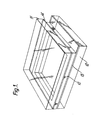
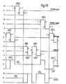
- a hermetically sealed envelope for a liquid crystal layer is formed by securing together two glass sheets 11 and 12 with a perimeter seal 13.
- the inward facing surfaces of the two sheets carry transparent electrode layers 14 and 15 of indium tin oxide, and each of these electrode layers is covered within the display area defined by the perimeter seal with a polymer layer, such as polyimide (not shown), provided for molecular alignment purposes.
- a polymer layer such as polyimide (not shown)
- Both polyimide layers are rubbed in a single direction so that when a liquid crystal is brought into contact with them they will tend to promote planar alignment of the liquid crystal molecules in the direction of the rubbing.
- the cell is assembled with the rubbing directions aligned parallel with each other.
- each one is patterned to define a set of strip electrodes (not shown) that individually extend across the display area and on out to beyond the perimeter seal to provide contact areas to which terminal connection may be made.
- the electrode strips of layer 14 extend transversely of those of layer 15 so as to define a pixel at each elemental area where an electrode strip of layer 15 is overlapped by a strip of layer 14.
- the thickness of the liquid crystal layer contained within the resulting enevelope is determined by the thickness of the perimeter seal, and control over the precision of this may be provided by a light scattering of short lengths of glass fibre (not shown) of uniform diameter distributed through the material of the perimeter seal.
- the cell is filled by applying a vacuum to an aperture (not shown) through one of the glass sheets in one corner of the area enclosed by the perimeter seal so as to cause the liquid crystal medium to enter the cell by way of another aperture (not shown) located in the diagonally opposite corner. (Subsequent to the filling operation the two apertures are sealed).
- the filling operation is carried out with the filling material heated into its isotropic phase so as to reduce its viscosity to a suitably low value.
- the basic construction of the cell is similar to that of for instance a conventional twisted nematic, except of course for the parallel alignment of the rubbing directions.
- the thickness of the perimeter seal 13, and hence of the liquid crystal layer is about 10 microns, but thinner or thicker layer thicknesses may be required to suit particular applications depending for instance upon whether or not bistability of operation is required and upon whether the layer is to be operated in the S* C phase or in one of the more ordered phases such as S* I or S* F .
- Both types of data pulse 21a and 21b have a total duration of 4t S , starting t S before the beginning of the positive excursion of a strobe pulse, and ending t S after the end of its negative-going excursion.
- a data '1' pulse 21a commences by making a positive-going excursion to a voltage +V D for a duration t S , a negative-going excursion to a voltage -V D for a duration 2t s , and finally a positive-going excursion to +V D for a duration t S .
- a data '0' pulse 21b is the inverse of the data '1' pulse.
- the potential difference developed across the liquid crystal layer at a pixel addressed by the coincidence of a strobe pulse 20 with a data '1' pulse 21a is given by the pulse waveform 22a, while that of 22b is that which is produced at a pixel addressed by the coincidence of a strobe pulse 20 with a data '0' pulse 21b.
- the pixel is addressed by a voltage of duration t s and of magnitude
- V S and V D are chosen so that the pixel is appropriately switched by the
- the data employed to address the immediately preceding and immediately following lines may be such as to produce a pair of reverse polarity pulses of magnitude
- the strobe and data pulse waveforms allow individual pixels to be switched in either direction that is data entry can be used to drive into the data '1' state selected pixels that were previously in the data '0' state, while at the same time other pixels that were previously in the '1' state are switched into the '0' state.
- the waveforms are charge balanced. These features are however attained at the expense of a line address time of 4t s even though the switching voltage magnitude
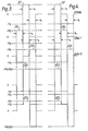
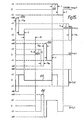
- FIG. 3 depicts waveforms according to one preferred embodiment of the present invention. Strobing, data '1' and data '0' pulse waveforms are depicted respectively at 30, 31a and 31b.
- the data pulse waveforms are applied in parallel to the electrode strips of one of the electrode layers 14, 15 while the strobe pulses are applied serially to those of the other electrode layer.
- a strobe pulse 30 is a balanced bipolar pulse having a negative-going voltage excursion to -V S following immediately after a positive-going one to +V S , both excursions being of duration t S .
- the data pulses 31a and 31b are balanced bipolar pulses, each having negative- and positive-going excursions of magnitude IVD and duration t S .
- these excursions are separated by a zero voltage portion, also of duration t S ; while in the case of the data '1' waveform 31a, the negative-going excursion follows on immediately after the positive-going excursion, and is itself followed by a zero voltage portion of duration t s .
- the potential difference developed across the liquid crystal layer at a pixel addressed by the coincidence of a strobe pulse 30 with a data '1' pulse 31a is given by the pulse waveform 32a, while that of 32b is that which is produced at a pixel addressed by the coincidence of a strobe pulse 30 with a data '0' pulse 31b.
- the pixel is addressed by a voltage of duration t s and magnitude
- V S and V D are chosen so that the pixel is appropriately switched by the
- the data employed to address the immediately preceding and immediately following lines may be such as to produce a single additional reverse polarity pulse of magnitude
- Figure 4 depicts the waveforms according to an alternative preferred embodiment of the present invention. Strobing data '1' and data '0' pulse waveforms are depicted respectively at 40, 41a and 41b, with the resultant potentials developed across an addressed pixel being given by waveforms 42a and 42b. These waveforms are derivable from those of Figure 3 by interchange of the roles of the first and second thirds of each waveform. A reason for making this interchange is that under the condition
- the line address time is 3t S , the value of which is related to the magnitude of the full switching voltage V S + V D
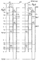
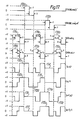
- the strobe pulse waveforms are depicted respectively at 50 and 60, the data '1' waveforms respectively at 51a and 61a, the data '0' waveforms respectively at 51b and 61b, and the resultant potentials developed across an addressed pixel at 52a, 52b, 62a, and 62b.
- the duration of each of the zero voltage steps t 01 , t 02 and t 03 is approximately 60% of the duration t S .
- the introduction of the zero voltage steps of Figures 5 and 6 increases the line address time beyond 3t S .
- a reduction in line address time is sometimes possible by the adoption of the expedient now to be described with reference to Figures 7 and 8.
- the strobe pulse waveforms of Figures 3 and 4 are modified by the shortening of the zero voltage portions of the strobe pulses 30 and 40 by a factor 'm' to give strobe pulses 70 and 80.
- the corresponding portions of the data pulse waveforms 31a, 31b, 41a and 41b are similarly shortened while their magnitudes are increased in the same proportion so as to retain charge balance.
- the resulting asymmetric, but charge balanced, bipolar data '1' and data '0' waveforms are depicted at 71a, 71b, 81a, and 81b.
- the resultant potentials developed across an addressed pixel are given by waveforms 72a, 72b, 82a and 82b respectively.
- the factor 'm' is typically not more than 3.
- the line address time is reduced by the use of these asymmetric waveforms from 3t s to (2 + 1/m) t S .
- the waveforms of Figures 5 and 6 are distinguished from those of Figures 3 and 4 by the introduction of zero voltage steps t 01 , t 02 and t 03 designed to prevent any switching stimulus from ever being immediately preceded by a reverse polarity stimulus or immediately followed by it, and thus to relax the switching criteria.
- a similar relaxation in the switching criteria for the waveforms of Figure 2 is achieved by the introduction of similar zero voltage steps as depicted in Figure 11.
- Figure 12 shows a similar modification applied to the waveforms of Figure 3 of Patent Specification No. 2146473A.
- the strobe pulse waveforms are depicted respectively at 110 and 120, the data '1' waveforms at llla and 121a, the data '0' waveforms at lllb and 121b, and the resultant potentials developed across an addressed pixel at 112a, 112b, 122a and 122b.
- Figure 13 depicts waveforms according to yet another preferred embodiment. Pairs of strobe, data '1' and data '0' waveforms are depicted respectively at 130a, 130b, 131a, 131b, 132a and 132b.
- the data waveforms are applied in parallel to the electrode strips of one of the electrode layers 14, 15, while strobe pulses are applied serially to those of the other electrode layer.
- each of the three types of pulse waveform has the same profile.
- This waveform is balanced bipolar, and involves making positive-going voltage excursion to +V for a duration 't' followed immediately by a negative-going voltage excursion to -V for a further duration 't'.
- the appropriate data pulses are arranged to bracket the application of the strobe pulse, with data '1' waveforms 131 immediately preceding the strobe pulse 130, and data '0' waveforms 132 immediately following the strobe pulse.
- 'V' and 't' are chosen so that a pulse of amplitude 'V' maintained for a duration 2t is sufficient to switch a pixel in the state determined by the direction in which that potential is applied, while a pulse of amplitude 'V' maintained for a duration of only 't' is insufficient for this purpose.
- FIG 13 the strobe pulse waveforms for rows 'p' and 'p+l' are depicted respectively at 130a and 130b.
- the pixel (p,q) defined by the intersection of row 'p' with column 'q' is set into, or maintained in, the data '1' state by the co-operative action of the strobe pulse waveform 130a to row 'p', with the data '1' pulse waveform 131a applied to column '1' immediately prior to the application of that strobe pulse.
- the pixel (p,r) defined by the intersection of row 'p' with column 'r' is set into, or maintained in, the data '0' state by the co-operative action of the strobe pulse waveform 130a applied to row 'p' and the data '0' pulse waveform 132a applied to column 'r'.
- the minimum period elapsing between the end of one strobe pulse and the beginning of the next is 4t.
- Data pulse waveforms 131b and 132b co-operate with strobe pulse waveform 130b applied to row 'p+1' to set pixels (p+1, q) and (p+1, r) respectively into the data '1' and data '0' states (or, if they are already respectively in those states, to maintain them in those states).
- the strobe and data pulse waveforms of Figure 13 produce a switching stimulus of 'V' maintained for a duration 2t. Inspection of the Figure 13 waveform shows however that each switching stimulus is both immediately preceded by and immediately followed by reverse polarity stimuli. Under appropriate conditions, the magnitude of 'V' or of 't' or even of both 'V' and 't' can be reduced if this sort of reverse polarity stimulus can be eliminated. This is achieved with the waveforms of Figure 14. These waveforms leave the same magnitude of reverse polarity stimulus as those of Figure 13, but separate such stimuli from the switching stimuli by the introduction of zero voltage steps of duration t 0 between the positive- and negative-going excursions of the strobe pulses and of both significances of data pulse.
- Strobe pulse waveforms for rows 'p' and 'p+l' are depicted respectively at 140a and 140b.
- Data '1' pulse waveforms are depicted at 141a and 141b respectively for columns 'q' and 'r', while data '0' pulse waveforms are depicted at 142a and 142b respectively for columns 'r' and 'q'.
- the potentials developed across the liquid crystal layer at pixels (p+1, q) and (p+1, r) as a result of the waveforms are depicted respectively at 143 and 144.
- the duration to of each of these zero voltage steps is not more than 50% of the duration t of a single voltage excursion.
- the minimum line address time is seen to be 3(2t+t 0 ). Superficially this appears longer than the minimum line address time of 6t achieved with the waveforms of Figure 13, but it must be remembered that the object of introducing the zero voltage steps was to ease switching, and so the value of 't' is not necessarily the same in the two instances.
- the strobe and data pulse waveforms of Figures 13 and 14 are composed of balanced bipolar pulses, and this is a necessary requirement. However, it is not necessary for the positive- and negative-going excursions of a data pulse to be of the same amplitude and duration.
- the waveforms of Figure 15 are distinguished from those of figure 13 by using asymmetric data pulses.
- the positive-going excursion of a data '1' pulse and the negative-going excursion of a data '0' pulse are 'm' times the amplitude and 1/m th the duration of their oppositely directed voltage excursions, where 'm' is some factor greater than unity.
- the strobe pulse waveform for row 'p+l' is depicted at 150.
- Data '1' pulse waveforms are depicted at 151a and 151b respectively for columns 'q' and 'r', while data '0' pulse waveforms are depicted at 152a and 152b respectively for columns 'r' and 'q'.
- the potentials developed across the liquid crystal layer at pixels (p+1, q) and (p+1, r) as a result of the waveforms are depicted respectively at 153 and 154.
- the minimum line address time in this instance is seen to be 2t(2 + 1/m).
- Waveforms 153 and 154 show that the reduction in minimum time address time achieved by the adoption of the waveforms of Figure 15 produces reverse polarity stimuli immediately preceding or immediately following the switching stimulus that are stronger than those obtained with the waveforms of Figure 13, albeit of shorter duration.
- the effect of these reverse polarity stimuli can be reduced by the insertion of zero voltage steps into the waveforms after the manner previously described with reference to Figure 14.
- the result is the waveforms of Figure 16.
- a zero voltage step of duration t 01 is inserted between the positive- and negative-going excursions of data pulses, while a similar zero voltage step of duration t 02 is inserted between those of both significances of data pulse.
- the durations t 01 and t 02 may be equal, but are not necessarily so.
- the strobe pulse waveform for row 'p+1' is depicted at 160.
- Data '1' pulse waveforms are depicted at 161a and 161b respectively for columns 'q' and 'r', while data '0' pulse waveforms are depicted respectively at 162a. and 162b respectively for columns 'r' and 'q'.
- the potentials developed across the liquid crystal layer at pixels (p+1, q) and (p+1, r) as a result of the waveforms are depicted respectively at 163 and 164.
- the minimum line address time in this instance is seen to be 2t(2 + 1/ m ) + t 01 + 2t 02 .
- each data pulse individually brackets a strobe pulse.
- the leading part of a data pulse the part before a strobe pulse, co-operates with a strobe pulse to set the relevant pixel into the data '1' state, or maintain it in that state if it was already in the data '1' state.
- the trailing part of the data pulse leaves the pixel in the data '1' state if it is a data '1' pulse waveform, or resets it into the data '1' state if it is a data '0' pulse waveform.
- the trailing part of the data pulse waveform simultaneously forms the leading part of the data pulse waveform for the next strobe pulse.
- Strobe pulse waveforms for rows 'p' and 'p+1' are depicted respectively at 170a and 170b. These consist of a positive-going excursion to a voltage +V for a duration 't' which is followed immediately by a negative-going excursion for a further duration 't'.
- a data pulse waveform is formed in two halves each of which exists in two forms 171a and 171b.
- the half data pulse waveform 171a consists of a zero voltage section of duration t 0 followed by a positive-going excursion to +V for a duration 't', which is immediately followed by a negative-going excursion to -V for a further duration 't'.
- the half data pulse waveform 171b is like that of waveform 171b except that the zero voltage section now lies between the positive- and negative-going excursions instead of ahead of them.
- the interval between consecutive strobe pulses is equal to the duration of a half data pulse waveform 171a or 171b.
- the potentials developed across the liquid crystal layer at pixels (p, q), (p, r), (p+1, q) and (p+1, r) as a result of the waveforms are depicted respectively at 174,- 175, 176 and 177.
- Pulse waveform 171a applied to column 'q' immediately before strobe pulse 170a therefore co-operates with the first half of that strobe pulse to produce at pixel (p,q) a voltage excursion 172a to +V lasting for a duration 2t.
- pulse waveform 171a is replaced by pulse waveform 171b, as occurs for instance in the production of the voltage excursion 172b at pixel (p,r).
- the voltage excursion 172a is followed by a reverse polarity excursion to -V that is maintained for a duration of only 't', and therefore pixel (p,q), having been set into the data '1' state by voltage excursion 172a, remains set in the data '1' state.
- the voltage excursion 172a is followed by a reverse polarity voltage excursion 172c to -V that is maintained for a duration of 2t, and therefore in this instance the pixel (p,r), having first been set into the data '1' state by the voltage excursion 172a, is then immediately rest back into the data '0' state by voltage excursion 172c.
- the waveforms co-operate to set pixel (p+l,r) into the data '1' state by the voltage excursion 173a, whereas they co-operate to set pixel (p+l,r) first into the data '1' state by the voltage excursion 173b, and then immediately back into the data '0' state by the voltage excursion 173c.
- voltage excursions 172a and 173b are immediately preceded by reverse polarity voltage excursions, and are also immediately followed by reverse polarity voltage excursions.
- voltage excursions 172c and 173c are immediately preceded by reverse polarity voltage excursions, but are not immediately followed by reverse polarity excursions.
- Figure 18 shows how the waveforms of Figure 17 may be modified by the lengthening of the strobe and data pulse waveforms by the inclusion of additional zero voltage sections so as to prevent reverse polarity excursions from immediately preceding or immediately following any switching stimulus.
- Strobe pulse waveforms 180 consist of positive- and negative-going voltage excursions, respectively to +V and -V, each of duration 't' which are separated by a zero voltage section of duration t 02 .
- a half data pulse waveform 181a consists of a zero voltage section of duration t 01 immediately followed by positive- and negative-going excursions, respectively to +V and -V, each of duration 't', which are separated by a zero voltage section of duration t 03 .
- a half data pulse waveform 181b consists of positive- and negative-going voltage excursions, respectively to +V and -V, each of duration 't' which are separated by a zero voltage section of duration (t 01 + t 03 ).
- Consecutive strobe pulse are separated in time by the duration of a half data pulse waveform 181a and 181b.
- the potentials developed across the liquid crystal layer at pixels (p,q), (p,r), (p+1, q) and (p+1, r) as a result of the waveforms are depicted respectively at 184, 185, 186 and 187.
- the waveforms leave these pixels respectively in data states '1', '0', '0' and '1'.
Abstract
Description
- This invention relates to the addressing of matrix array type ferroelectric liquid crystal cells.
- Hitherto dynamic scattering mode liquid crystal cells have been operated using a d.c. drive or an a.c. one, whereas field effect mode liquid crystal devices have generally been operated using an a.c. drive in order to avoid performance impairment problems associated with electrolytic degradation of the liquid crystal layer. Such devices have employed liquid crystals that do not exhibit ferroelectricity, and the material interacts with an applied electric field by way of an induced dipole. As a result they are not sensitive to the polarity of the applied field, but respond to the applied RMS voltage averaged over approximately one response time at that voltage. There may also be frequency dependence as in the case of so-called two-frequency materials, but this only affects the type of response produced by the applied field.
- In contrast to this, a ferroelectric liquid crystal exhibits a permanent electric dipole, and it is this permanent dipole which will interact with an applied electric field. Ferroelectric liquid crystals are of interest in display, switching and information processing applications because they are expected to show a greater. coupling with an applied field than that typical of a liquid crystal that relies on coupling with an induced dipole, and hence ferroelectric liquid crystals are expected to show a faster response. A ferroelectric liquid crystal display mode is described for instance by N.A. Clark et al in a paper entitled 'Ferro-electric Liquid Crystal Electro-Optics using the Surface Stabilized Structure' appearing in Mol. Cryst. Liq. Cryst. 1983 Volume 94 pages 213 to 234. By way of example reference may also be made to an alternative mode that is described in the specification of British Patent Application No. 8426976.
- A particularly significant characteristic peculiar to ferroelectric smectic cells is the fact that they, unlike other types of liquid crystal cell, are responsive differently according to the polarity of the applied field. This characteristic sets the choice of a suitable matrix-addressed driving system for a ferroelectric smectic into a class of its own. A further factor which can be significant is that, in the region of switching times of the order of a microsecond, a ferroelectric smectic typically exhibits a relatively weak dependence of its switching time upon switching voltage. In this region the switching time of a ferroelectric may typically exhibit a response time proportional to the inverse square of applied voltage or, even worse, proportional to the inverse single power of voltage. In contrast to this, a (non-ferroelectric) smectic A device, which in certain other respects is a comparable device exhibiting a long-term storage capability, exhibits in a corresponding region of switching speeds a response time that is typically proportional to the inverse fifth power of voltage. The significance of this difference becomes apparent when it is appreciated first that there is a voltage threshold beneath which a signal will never produce switching however long that signal is maintained; second that for any chosen voltage level above this voltage threshold there is a minimum time ts for which the signal has to be maintained to effect switching; and third that at this chosen voltage level there is a shorter minimum time tp beneath which the application of the signal voltage produces no persistent effect, but above which, upon removal of the signal voltage, the liquid crystal does not revert fully to the state subsisting before the signal was applied. When the relationship ts = f(V) between V and ts is known, a working guide to the relationship between V and tp is often found to be given by the curve tp = g(V) formed by plotting (Vl,t2) where the points (V1, t1 and V2,t2) lie on the ts - f(V) curve, and where tl = 10t2. Now the ratio of V2/V1 is increased as the inverse dependence of switching time upon applied voltage weakens, and hence, when the working guide is applicable, a consequence of weakened dependence is an increased intolerance of the system to the incidence of wrong polarity signals to any pixel, that is signals tending to switch to the '1' state a pixel intended to be left in the '0' state, or to switch to the '0' state a pixel intended to be left in the '1' state.
- Therefore, a good drive scheme for addressing a ferroelectric liquid crystal cell must take account of polarity, and may also need to take particular care to minimise the incidence of wrong polarity signals to any given pixel whether it is intended as '1' state pixel or a '0' state one. Additionally, the waveforms applied to the individual electrodes by which the pixels are addressed need to be charge-balanced at least in the long term. If the electrodes are not insulated from the liquid crystal this is so as to avoid electrolytic degradation of the liquid crystal brought about by a net flow of direct current through the liquid crystal. On the other hand if the electrodes are insulated, it is to prevent a cumulative build up of charge at the interface between the liquid crystal and the insulation.
- With these considerations in mind a number of methods for addressing matrix-array type ferroelectric liquid crystal cells are described in Patent Specification No. 2146473A to which attention is directed. In particular there is an addressing method described with reference to Figure 2 of that specification which employs balanced bipolar strobe pulses in conjunction with balanced bipolar data pulses for the addressing of the cell. In that particular adressing method the strobe pulse voltage is switched between +VS and -VS and the data pulse voltage is switched between +VD and -VD. These voltages co-operate to produce a potential difference of (Vs + VD) across the thickness of the liquid crystal layer of the cell for a
duration t s2 and it is arranged that this will be sufficient to effect switching of any pixel to which this signal is applied. The shape and timing of the strobe and data pulses is arranged so that at no time will a pixel see a wrong polarity signal having a magnitude exceeding |VS - VD|, or |VD|, whichever is the greater. By this means is facilitated the achieving of low maximum magnitude of reverse polarity signals, but this is achieved at the expense of a line address time of 4tS. - The present invention is concerned with modifying the waveforms with a view to reducing the minimum line address time for a given adress voltage, albeit that this is achieved at the expense of an exposure to larger reverse polarity signals. In this context it can be shown that certain configurations of cell with certain mixtures ferroelectric liquid crystal fillings exhibit a switching behaviour that is much more tolerant of reverse polarity voltages than is implied by the above-quoted working guide, for instance producing no persistent effect when addressed with a reverse polarity pulse of the same duration but only 75% of the amplitude of a pulse that is just sufficient to effect switching.
- According to the present invention a method of addressing a matrix-array type liquid crystal cell with a ferroelectric liquid crystal layer whose pixels are defined by the areas of overlap between the members of a first set of electrodes on one side of the liquid crystal layer and the members of a second set on the other side of the layer, is characterised in that the cell is addressed on a line-by-line basis by applying strobe pulses serially to the members of the first set while data pulses are applied in parallel to the members of the second set, that the strobe and data pulse waveforms are balanced bipolar pulses, and that the adressing of any given pixel by the co-operative action of a strobe pulse of a data pulse waveform includes a zero voltage step during at least a part of the strobe pulse.
- There follows a description of a ferroelectric liquid crystal cell and of a number of ways by which it may be addressed. With the exception of the first method, which has been included for the purposes of comparison, all these methods embody the present invention in preferred forms. The first method is one of the methods described in Patent Specification No. 2146473A. The description refers to the accompanying drawings in which:-
- Figure 1 depicts a schematic perspective view of a ferroelectric liquid crystal cell;
- Figure 2 depicts the waveforms of a drive scheme previously described in Patent Specification No. 2146473A, and
- Figures 3 to 18 depict the waveforms of sixteen alternative drive schemes embodying the invention in preferred forms.
- Referring now to Figure 1, a hermetically sealed envelope for a liquid crystal layer is formed by securing together two
glass sheets 11 and 12 with aperimeter seal 13. The inward facing surfaces of the two sheets carrytransparent electrode layers electrode layers layer 14 extend transversely of those oflayer 15 so as to define a pixel at each elemental area where an electrode strip oflayer 15 is overlapped by a strip oflayer 14. The thickness of the liquid crystal layer contained within the resulting enevelope is determined by the thickness of the perimeter seal, and control over the precision of this may be provided by a light scattering of short lengths of glass fibre (not shown) of uniform diameter distributed through the material of the perimeter seal. Conveniently the cell is filled by applying a vacuum to an aperture (not shown) through one of the glass sheets in one corner of the area enclosed by the perimeter seal so as to cause the liquid crystal medium to enter the cell by way of another aperture (not shown) located in the diagonally opposite corner. (Subsequent to the filling operation the two apertures are sealed). The filling operation is carried out with the filling material heated into its isotropic phase so as to reduce its viscosity to a suitably low value. It will be noted that the basic construction of the cell is similar to that of for instance a conventional twisted nematic, except of course for the parallel alignment of the rubbing directions. - Typically the thickness of the
perimeter seal 13, and hence of the liquid crystal layer, is about 10 microns, but thinner or thicker layer thicknesses may be required to suit particular applications depending for instance upon whether or not bistability of operation is required and upon whether the layer is to be operated in the S*C phase or in one of the more ordered phases such as S*I or S*F. - Some drive schemes for ferroelectric cells are described in Patent Specification No. 2146473A. Among these is a scheme that is described with particular reference to Figure 2 of that specification, a part of which has been reproduced herein in slightly modified form as Figure 2 of this specification. This employs balanced bipolar data pulses 21a, 21b to co-act with balanced
bipolar strobe pulses 20. Thestrobe pulses 20 are applied serially to the electrode strips of one electrode layer, while the data pulses 21a and 21b are applied in parallel to those of the other layer. In this particular scheme astrobe pulse 20 makes an excursion to a voltage +VS for a duration tS, and then immediately an excursion to a voltage -VS for a further duration ts. Both types of data pulse 21a and 21b have a total duration of 4tS, starting tS before the beginning of the positive excursion of a strobe pulse, and ending tS after the end of its negative-going excursion. A data '1' pulse 21a commences by making a positive-going excursion to a voltage +VD for a duration tS, a negative-going excursion to a voltage -VD for a duration 2ts, and finally a positive-going excursion to +VD for a duration tS. A data '0' pulse 21b is the inverse of the data '1' pulse. It starts with a negative-going excursion to -VD for a duration tS, follows this with an excursion to +VD for a duration 2ts, and terminates with an excursion back to -VD for a duration tS. - The potential difference developed across the liquid crystal layer at a pixel addressed by the coincidence of a
strobe pulse 20 with a data '1' pulse 21a is given by the pulse waveform 22a, while that of 22b is that which is produced at a pixel addressed by the coincidence of astrobe pulse 20 with a data '0' pulse 21b. In each instance the pixel is addressed by a voltage of duration ts and of magnitude |VS + VD| tending to switch the pixel in the required direction, but it is also addressed by two reverse polarity pulses of magnitude |VD| , and one of magnitude |VS - VD| , tending to switch it in the wrong direction. The values of VS and VD are chosen so that the pixel is appropriately switched by the |VS + VD| magnitude pulse without this switching being negated by the reverse polarity pulses. In considering the effect of reverse polarity pulses upon a given pixel it should also be noted that the data employed to address the immediately preceding and immediately following lines may be such as to produce a pair of reverse polarity pulses of magnitude |VD| and net duration ts that immediately precede and follow the voltage waveform produced by the addressing of the given pixel. - The strobe and data pulse waveforms allow individual pixels to be switched in either direction that is data entry can be used to drive into the data '1' state selected pixels that were previously in the data '0' state, while at the same time other pixels that were previously in the '1' state are switched into the '0' state. The waveforms are charge balanced. These features are however attained at the expense of a line address time of 4ts even though the switching voltage magnitude |VS + VD| is capable of switching a pixel in a quarter of this time.
- Attention will now be turned to Figure 3 which depicts waveforms according to one preferred embodiment of the present invention. Strobing, data '1' and data '0' pulse waveforms are depicted respectively at 30, 31a and 31b.
- As before, the data pulse waveforms are applied in parallel to the electrode strips of one of the electrode layers 14, 15 while the strobe pulses are applied serially to those of the other electrode layer.
- A
strobe pulse 30 is a balanced bipolar pulse having a negative-going voltage excursion to -VS following immediately after a positive-going one to +VS, both excursions being of duration tS. - The data pulses 31a and 31b are balanced bipolar pulses, each having negative- and positive-going excursions of magnitude IVD and duration tS. In the case of the data '0' waveform 31b, these excursions are separated by a zero voltage portion, also of duration tS; while in the case of the data '1' waveform 31a, the negative-going excursion follows on immediately after the positive-going excursion, and is itself followed by a zero voltage portion of duration ts.
- The potential difference developed across the liquid crystal layer at a pixel addressed by the coincidence of a
strobe pulse 30 with a data '1' pulse 31a is given by the pulse waveform 32a, while that of 32b is that which is produced at a pixel addressed by the coincidence of astrobe pulse 30 with a data '0' pulse 31b. In each instance the pixel is addressed by a voltage of duration ts and magnitude |VS + VD| tending to switch the pixel in the required direction, but it is also addressed by reverse polarity pulses of magnitude |VS and VD| , both of duration tS, tending to switch the pixel in the wrong direction. The values of VS and VD are chosen so that the pixel is appropriately switched by the |VS + VD| magnitude pulse without this switching being negated by the reverse polarity pulses. In considering the effect of reverse polarity pulses upon a given pixel it should also be noted that the data employed to address the immediately preceding and immediately following lines may be such as to produce a single additional reverse polarity pulse of magnitude |VD| and duration tS that either immediately precedes or immediately follows the voltage waveform produced by the addressing of the given pixel. - Thus these strobe and data pulse waveforms of Figure 3 co-operate to provide a shorter line address time than those of Figure 2, 3tS instead of 4tS. This saving of time is obtained at the expense of exposing the pixel to a reverse polarity pulses of magnitude |VS and VD|, whereas with the Figure 2 waveforms the reverse polarity pulses have magnitudes of |VS - VD| and |VD| . The reverse polarity pulse of magnitude |VS| is more significant than the others whenever |VS| > 2| VD| a condition which is generally satisfied in practice.
- Figure 4 depicts the waveforms according to an alternative preferred embodiment of the present invention. Strobing data '1' and data '0' pulse waveforms are depicted respectively at 40, 41a and 41b, with the resultant potentials developed across an addressed pixel being given by waveforms 42a and 42b. These waveforms are derivable from those of Figure 3 by interchange of the roles of the first and second thirds of each waveform. A reason for making this interchange is that under the condition |VS| > 2 | VD the reverse polarity pulse that immediately precedes exposure of a pixel to +(VS + VD), or that immediately follows the exposure of a pixel to -(VS + VD) is reduced in magnitude from |VS| to |VD|.
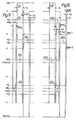
- When using either the waveforms of Figure 3, or those of Figure 4, the line address time is 3tS, the value of which is related to the magnitude of the full switching voltage VS + VD| . It has been found however that in some circumstances the minimum conditions for achieving switching are adversely affected if the switching stimulus is immediately followed or immediately preceded by a stimulus of the opposite polarity. Inspection of waveforms 32a and 32b reveals for instance that with the Figure 3 waveforms the switching stimulus is always immediately preceded with a stimulus of the opposite polarity. At least under some conditions the switching criteria can be somewhat relaxed, for instance to allow a shortening of the duration ts or a reduction of the switching voltage (Vs + VD). This may be achieved by introducing zero voltage steps of duration t01, t 02 and t03 between each consecutive third of the waveforms of Figures 3 and 4 to produce waveforms as depicted in Figures 5 and 6. In these Figures the strobe pulse waveforms are depicted respectively at 50 and 60, the data '1' waveforms respectively at 51a and 61a, the data '0' waveforms respectively at 51b and 61b, and the resultant potentials developed across an addressed pixel at 52a, 52b, 62a, and 62b. Typically the duration of each of the zero voltage steps t01, t 02 and t03 is approximately 60% of the duration tS.
- The introduction of the zero voltage steps of Figures 5 and 6 increases the line address time beyond 3tS. A reduction in line address time is sometimes possible by the adoption of the expedient now to be described with reference to Figures 7 and 8. The strobe pulse waveforms of Figures 3 and 4 are modified by the shortening of the zero voltage portions of the
strobe pulses strobe pulses - The use of these asymmetric waveforms may also be combined with the use of the zero voltage gaps described previously with particular reference to Figures 5 and 6. The resulting waveforms are depicted in Figures 9 and 10, in which the strobe pulse waveforms are depicted at 90 and 100, the data '1' pulse waveforms at 91a and 101a, the data '0' pulse waveforms at 91b and 101b, and the resultant potentials developed across an addressed pixel at 92a, 92b, 102a and 102b.
- The waveforms of Figures 5 and 6 are distinguished from those of Figures 3 and 4 by the introduction of zero voltage steps t01, t02 and t03 designed to prevent any switching stimulus from ever being immediately preceded by a reverse polarity stimulus or immediately followed by it, and thus to relax the switching criteria. A similar relaxation in the switching criteria for the waveforms of Figure 2 is achieved by the introduction of similar zero voltage steps as depicted in Figure 11. Figure 12 shows a similar modification applied to the waveforms of Figure 3 of Patent Specification No. 2146473A. In these Figures the strobe pulse waveforms are depicted respectively at 110 and 120, the data '1' waveforms at llla and 121a, the data '0' waveforms at lllb and 121b, and the resultant potentials developed across an addressed pixel at 112a, 112b, 122a and 122b.
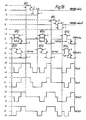
- Attention will now be turned to Figure 13 which depicts waveforms according to yet another preferred embodiment. Pairs of strobe, data '1' and data '0' waveforms are depicted respectively at 130a, 130b, 131a, 131b, 132a and 132b. As with the previous embodiments, so with this one, the data waveforms are applied in parallel to the electrode strips of one of the electrode layers 14, 15, while strobe pulses are applied serially to those of the other electrode layer. In this instance each of the three types of pulse waveform has the same profile. This waveform is balanced bipolar, and involves making positive-going voltage excursion to +V for a duration 't' followed immediately by a negative-going voltage excursion to -V for a further duration 't'. In order to address any given line of pixels the appropriate data pulses are arranged to bracket the application of the strobe pulse, with data '1' waveforms 131 immediately preceding the strobe pulse 130, and data '0' waveforms 132 immediately following the strobe pulse.
- The values of 'V' and 't' are chosen so that a pulse of amplitude 'V' maintained for a duration 2t is sufficient to switch a pixel in the state determined by the direction in which that potential is applied, while a pulse of amplitude 'V' maintained for a duration of only 't' is insufficient for this purpose.
- In Figure 13 the strobe pulse waveforms for rows 'p' and 'p+l' are depicted respectively at 130a and 130b. The pixel (p,q) defined by the intersection of row 'p' with column 'q' is set into, or maintained in, the data '1' state by the co-operative action of the
strobe pulse waveform 130a to row 'p', with the data '1'pulse waveform 131a applied to column '1' immediately prior to the application of that strobe pulse. Similarly the pixel (p,r) defined by the intersection of row 'p' with column 'r' is set into, or maintained in, the data '0' state by the co-operative action of thestrobe pulse waveform 130a applied to row 'p' and the data '0' pulse waveform 132a applied to column 'r'. The minimum period elapsing between the end of one strobe pulse and the beginning of the next is 4t.Data pulse waveforms strobe pulse waveform 130b applied to row 'p+1' to set pixels (p+1, q) and (p+1, r) respectively into the data '1' and data '0' states (or, if they are already respectively in those states, to maintain them in those states). - The potentials developed across the liquid crystal layer at pixels (p+1, q) and (p+1, r) as a result of these waveforms are depicted respectively at 133 and 134. Remembering that the row and column voltages are applied to opposite sides of the liquid crystal layer, the data '1'
pulse waveform 131a is inverted in thewaveform trace 133 at 131a'. It has no switching effect because the positive and negative voltage excursions each last only for a duration 't'. In contrast to this, the data '0'pulse waveform 132b inverted at 32b' inwaveform trace 133, provides in its first half a voltage excursion of the same polarity as that of the second half of thestrobe pulse 130b that immediately precedes it. The result is that at 135 inwaveform trace 133 pixel (p+1, q) is exposed to the voltage -V for a duration 2t, and this is sufficient to effect switching into the data '0' state. Similarly intrace 134 the inversion of the data '1'pulse 131b produces a positive going excursion which is followed immediately by the positive going excursion of the first half ofstrobe pulse 130b. The result is that at 136 inwaveform trace 134 pixel (p+1, r) is exposed to the voltage +V for a duration 2t. This causes this pixel to switch into the data '1' state. - Comparing the waveforms of Figures 2 and 13 it is seen that the minimum line address time with the Figure 2 waveforms is four times the minimum switching period tS, whereas with the Figure 13 waveforms it is only three times the minimum switching period '2t'.
- The strobe and data pulse waveforms of Figure 13 produce a switching stimulus of 'V' maintained for a duration 2t. Inspection of the Figure 13 waveform shows however that each switching stimulus is both immediately preceded by and immediately followed by reverse polarity stimuli. Under appropriate conditions, the magnitude of 'V' or of 't' or even of both 'V' and 't' can be reduced if this sort of reverse polarity stimulus can be eliminated. This is achieved with the waveforms of Figure 14. These waveforms leave the same magnitude of reverse polarity stimulus as those of Figure 13, but separate such stimuli from the switching stimuli by the introduction of zero voltage steps of duration t0 between the positive- and negative-going excursions of the strobe pulses and of both significances of data pulse. Strobe pulse waveforms for rows 'p' and 'p+l' are depicted respectively at 140a and 140b. Data '1' pulse waveforms are depicted at 141a and 141b respectively for columns 'q' and 'r', while data '0' pulse waveforms are depicted at 142a and 142b respectively for columns 'r' and 'q'. The potentials developed across the liquid crystal layer at pixels (p+1, q) and (p+1, r) as a result of the waveforms are depicted respectively at 143 and 144. Typically the duration to of each of these zero voltage steps is not more than 50% of the duration t of a single voltage excursion. The minimum line address time is seen to be 3(2t+t0). Superficially this appears longer than the minimum line address time of 6t achieved with the waveforms of Figure 13, but it must be remembered that the object of introducing the zero voltage steps was to ease switching, and so the value of 't' is not necessarily the same in the two instances.
- The strobe and data pulse waveforms of Figures 13 and 14 are composed of balanced bipolar pulses, and this is a necessary requirement. However, it is not necessary for the positive- and negative-going excursions of a data pulse to be of the same amplitude and duration. The waveforms of Figure 15 are distinguished from those of figure 13 by using asymmetric data pulses. The positive-going excursion of a data '1' pulse and the negative-going excursion of a data '0' pulse are 'm' times the amplitude and 1/mth the duration of their oppositely directed voltage excursions, where 'm' is some factor greater than unity. The strobe pulse waveform for row 'p+l' is depicted at 150. Data '1' pulse waveforms are depicted at 151a and 151b respectively for columns 'q' and 'r', while data '0' pulse waveforms are depicted at 152a and 152b respectively for columns 'r' and 'q'. The potentials developed across the liquid crystal layer at pixels (p+1, q) and (p+1, r) as a result of the waveforms are depicted respectively at 153 and 154. The minimum line address time in this instance is seen to be 2t(2 + 1/m).
-
Waveforms - With the waveforms of Figures 13, 14, 15 and 16 the data pulses bracket each strobe pulses, but an individual data pulse is either entirely ahead of the strobe pulse or entirely after it, according to data significance. Attention is now turned to the waveforms of Figure 17 in which each data pulse individually brackets a strobe pulse. The leading part of a data pulse, the part before a strobe pulse, co-operates with a strobe pulse to set the relevant pixel into the data '1' state, or maintain it in that state if it was already in the data '1' state. Then the trailing part of the data pulse leaves the pixel in the data '1' state if it is a data '1' pulse waveform, or resets it into the data '1' state if it is a data '0' pulse waveform. The trailing part of the data pulse waveform simultaneously forms the leading part of the data pulse waveform for the next strobe pulse.
- Strobe pulse waveforms for rows 'p' and 'p+1' are depicted respectively at 170a and 170b. These consist of a positive-going excursion to a voltage +V for a duration 't' which is followed immediately by a negative-going excursion for a further duration 't'. A data pulse waveform is formed in two halves each of which exists in two
forms 171a and 171b. The half data pulse waveform 171a consists of a zero voltage section of duration t0 followed by a positive-going excursion to +V for a duration 't', which is immediately followed by a negative-going excursion to -V for a further duration 't'. The halfdata pulse waveform 171b is like that ofwaveform 171b except that the zero voltage section now lies between the positive- and negative-going excursions instead of ahead of them. The interval between consecutive strobe pulses is equal to the duration of a halfdata pulse waveform 171a or 171b. The potentials developed across the liquid crystal layer at pixels (p, q), (p, r), (p+1, q) and (p+1, r) as a result of the waveforms are depicted respectively at 174,- 175, 176 and 177. - As before, the values of 'V' and 't' are chosen so that a pulse of amplitude 'V' maintained for a duration 2t is sufficient to switch a pixel in the state determined by the direction in which that potential is applied, while a pulse of amplitude 'V' maintained for a duration of only 't' is insufficient for this purpose. Pulse waveform 171a applied to column 'q' immediately before strobe pulse 170a therefore co-operates with the first half of that strobe pulse to produce at pixel (p,q) a voltage excursion 172a to +V lasting for a duration 2t. A similar effect is also obtained if pulse waveform 171a is replaced by
pulse waveform 171b, as occurs for instance in the production of thevoltage excursion 172b at pixel (p,r). In the case of pixel (p,q) the voltage excursion 172a is followed by a reverse polarity excursion to -V that is maintained for a duration of only 't', and therefore pixel (p,q), having been set into the data '1' state by voltage excursion 172a, remains set in the data '1' state. In the case of pixel (p,r), the voltage excursion 172a is followed by a reverse polarity voltage excursion 172c to -V that is maintained for a duration of 2t, and therefore in this instance the pixel (p,r), having first been set into the data '1' state by the voltage excursion 172a, is then immediately rest back into the data '0' state by voltage excursion 172c. Similarly the waveforms co-operate to set pixel (p+l,r) into the data '1' state by the voltage excursion 173a, whereas they co-operate to set pixel (p+l,r) first into the data '1' state by thevoltage excursion 173b, and then immediately back into the data '0' state by the voltage excursion 173c. - From examination of these waveforms it is seen that it is the form of the half data pulse waveform that immediately follows a strobe pulse that determines the data significance of the full data waveform at the pixel addressed by the coincidence of that waveform with the strobe pulse. Further it is seen that this data significance has itself no data significance in the addressing of the next row with the next strobe pulse, even though it does form part of the full data waveform used in the addressing of that next row.
- It may also be noted that
voltage excursions 172a and 173b are immediately preceded by reverse polarity voltage excursions, and are also immediately followed by reverse polarity voltage excursions. On the other hand the other two voltage excursions that determine the final state of an address pixel, voltage excursions 172c and 173c, are immediately preceded by reverse polarity voltage excursions, but are not immediately followed by reverse polarity excursions. Figure 18 shows how the waveforms of Figure 17 may be modified by the lengthening of the strobe and data pulse waveforms by the inclusion of additional zero voltage sections so as to prevent reverse polarity excursions from immediately preceding or immediately following any switching stimulus. -
Strobe pulse waveforms 180 consist of positive- and negative-going voltage excursions, respectively to +V and -V, each of duration 't' which are separated by a zero voltage section of duration t02. A half data pulse waveform 181a consists of a zero voltage section of duration t01 immediately followed by positive- and negative-going excursions, respectively to +V and -V, each of duration 't', which are separated by a zero voltage section of duration t03. A halfdata pulse waveform 181b consists of positive- and negative-going voltage excursions, respectively to +V and -V, each of duration 't' which are separated by a zero voltage section of duration (t01 + t03). Consecutive strobe pulse are separated in time by the duration of a halfdata pulse waveform 181a and 181b. The potentials developed across the liquid crystal layer at pixels (p,q), (p,r), (p+1, q) and (p+1, r) as a result of the waveforms are depicted respectively at 184, 185, 186 and 187. The waveforms leave these pixels respectively in data states '1', '0', '0' and '1'.
Claims (12)
Applications Claiming Priority (2)
| Application Number | Priority Date | Filing Date | Title |
|---|---|---|---|
| GB8508713 | 1985-04-03 | ||
| GB08508713A GB2173337B (en) | 1985-04-03 | 1985-04-03 | Addressing liquid crystal cells |
Publications (2)
| Publication Number | Publication Date |
|---|---|
| EP0197743A2 true EP0197743A2 (en) | 1986-10-15 |
| EP0197743A3 EP0197743A3 (en) | 1989-10-18 |
Family
ID=10577144
Family Applications (1)
| Application Number | Title | Priority Date | Filing Date |
|---|---|---|---|
| EP86302381A Withdrawn EP0197743A3 (en) | 1985-04-03 | 1986-04-01 | Addressing liquid crystal cells |
Country Status (5)
| Country | Link |
|---|---|
| US (1) | US4728947A (en) |
| EP (1) | EP0197743A3 (en) |
| JP (1) | JPS61286817A (en) |
| AU (1) | AU582636B2 (en) |
| GB (1) | GB2173337B (en) |
Cited By (10)
| Publication number | Priority date | Publication date | Assignee | Title |
|---|---|---|---|---|
| EP0240222A1 (en) * | 1986-04-01 | 1987-10-07 | Stc Plc | Addressing liquid crystal cells |
| EP0300754A2 (en) * | 1987-07-21 | 1989-01-25 | THORN EMI plc | Display device |
| WO1989001681A1 (en) * | 1987-08-12 | 1989-02-23 | The General Electric Company, Plc | Ferroelectric liquid crystal devices |
| WO1989005025A1 (en) * | 1987-11-18 | 1989-06-01 | The Secretary Of State For Defence In Her Britanni | Multiplex addressing of ferro-electric crystal displays |
| EP0370649A2 (en) * | 1988-11-23 | 1990-05-30 | Nortel Networks Corporation | Addressing scheme for multiplexed ferro-electric liquid crystal |
| EP0613116A2 (en) * | 1993-02-25 | 1994-08-31 | Seiko Epson Corporation | Method of driving a liquid crystal display device |
| WO1995024715A1 (en) * | 1994-03-07 | 1995-09-14 | The Secretary Of State For Defence In Her Britannic Majesty's Government Of The United Kingdom Of Great Britain And Northern Ireland | Temperature compensation of ferroelectric liquid crystal displays |
| GB2301450A (en) * | 1994-03-07 | 1996-12-04 | Secr Defence | Temperature compensation of ferroelectric liquid crystal displays |
| US6072558A (en) * | 1992-07-16 | 2000-06-06 | Seiko Epson Corporation | Electrooptical element switchable between a plurality of metabstable states |
| US6252571B1 (en) | 1995-05-17 | 2001-06-26 | Seiko Epson Corporation | Liquid crystal display device and its drive method and the drive circuit and power supply circuit device used therein |
Families Citing this family (23)
| Publication number | Priority date | Publication date | Assignee | Title |
|---|---|---|---|---|
| US4655561A (en) * | 1983-04-19 | 1987-04-07 | Canon Kabushiki Kaisha | Method of driving optical modulation device using ferroelectric liquid crystal |
| GB2173336B (en) * | 1985-04-03 | 1988-04-27 | Stc Plc | Addressing liquid crystal cells |
| GB2173335B (en) * | 1985-04-03 | 1988-02-17 | Stc Plc | Addressing liquid crystal cells |
| GB2175725B (en) * | 1985-04-04 | 1989-10-25 | Seikosha Kk | Improvements in or relating to electro-optical display devices |
| US4836656A (en) * | 1985-12-25 | 1989-06-06 | Canon Kabushiki Kaisha | Driving method for optical modulation device |
| US5255110A (en) * | 1985-12-25 | 1993-10-19 | Canon Kabushiki Kaisha | Driving method for optical modulation device using ferroelectric liquid crystal |
| JPS6373228A (en) * | 1986-09-17 | 1988-04-02 | Canon Inc | Method for driving optical modulating element |
| GB8623240D0 (en) * | 1986-09-26 | 1986-10-29 | Emi Plc Thorn | Display device |
| JPS63116128A (en) * | 1986-11-04 | 1988-05-20 | Canon Inc | Driving method for optical modulating element |
| GB2207272B (en) * | 1987-07-18 | 1991-08-14 | Stc Plc | Addressing liquid crystal cells |
| GB2208741B (en) * | 1987-08-12 | 1992-03-25 | Gen Electric Co Plc | Ferroelectric liquid crystal devices |
| GB8720856D0 (en) * | 1987-09-04 | 1987-10-14 | Emi Plc Thorn | Matrix addressing |
| US4870398A (en) * | 1987-10-08 | 1989-09-26 | Tektronix, Inc. | Drive waveform for ferroelectric displays |
| US4915477A (en) * | 1987-10-12 | 1990-04-10 | Seiko Epson Corporation | Method for driving an electro-optical device wherein erasing data stored in each pixel by providing each scan line and data line with an erasing signal |
| NL8703040A (en) * | 1987-12-16 | 1989-07-17 | Philips Nv | METHOD FOR CONTROLLING A PASSIVE FERRO-ELECTRIC LIQUID CRYSTAL DISPLAY. |
| US5963186A (en) * | 1990-08-07 | 1999-10-05 | The Secretary Of State For Defence In Her Britannic Majesty's Government Of The United Kingdom Of Great Britain And Northern Ireland | Multiplex addressing of ferro-electric liquid crystal displays |
| KR950000754B1 (en) * | 1992-04-30 | 1995-01-28 | 삼성전관 주식회사 | Driving method and vias voltage circuit of strong dielectric lcd using stn driving i. c. |
| GB9309502D0 (en) * | 1993-05-08 | 1993-06-23 | Secr Defence | Addressing ferroelectric liquid crystal displays |
| DE69514451T2 (en) * | 1994-03-18 | 2000-07-20 | Koninkl Philips Electronics Nv | DISPLAY DEVICE WITH ACTIVE MATRIX AND CONTROL PROCEDURE THEREFOR |
| GB9526270D0 (en) * | 1995-12-21 | 1996-02-21 | Secr Defence | Multiplex addressing of ferroelectric liquid crystal displays |
| GB9612958D0 (en) * | 1996-06-20 | 1996-08-21 | Sharp Kk | Matrix array bistable device addressing |
| US6987501B2 (en) * | 2001-09-27 | 2006-01-17 | Citizen Watch Co., Ltd. | Ferroelectric liquid crystal apparatus and method for driving the same |
| KR20050061532A (en) * | 2002-10-16 | 2005-06-22 | 코닌클리케 필립스 일렉트로닉스 엔.브이. | A display apparatus with a display device and method of driving the display device |
Citations (3)
| Publication number | Priority date | Publication date | Assignee | Title |
|---|---|---|---|---|
| GB2067332A (en) * | 1979-12-25 | 1981-07-22 | Seiko Instr & Electronics | Electro-optical display arrangements |
| GB2175725A (en) * | 1985-04-04 | 1986-12-03 | Seikosha Kk | Improvements in or relating to electro-optical display devices |
| EP0229647A2 (en) * | 1986-01-10 | 1987-07-22 | Hitachi, Ltd. | Liquid crystal matrix driving method |
Family Cites Families (27)
| Publication number | Priority date | Publication date | Assignee | Title |
|---|---|---|---|---|
| CH529421A (en) * | 1971-03-30 | 1972-10-15 | Bbc Brown Boveri & Cie | Circuit arrangement for controlling liquid-crystalline light valves which can be addressed in matrix form |
| JPS523560B1 (en) * | 1971-06-02 | 1977-01-28 | ||
| JPS5114434B1 (en) * | 1971-07-29 | 1976-05-10 | ||
| JPS5715393B2 (en) * | 1973-04-20 | 1982-03-30 | ||
| US3911421A (en) * | 1973-12-28 | 1975-10-07 | Ibm | Selection system for matrix displays requiring AC drive waveforms |
| JPS5416894B2 (en) * | 1974-03-01 | 1979-06-26 | ||
| US4048633A (en) * | 1974-03-13 | 1977-09-13 | Tokyo Shibaura Electric Co., Ltd. | Liquid crystal driving system |
| US4062626A (en) * | 1974-09-20 | 1977-12-13 | Hitachi, Ltd. | Liquid crystal display device |
| US4040720A (en) * | 1975-04-21 | 1977-08-09 | Rockwell International Corporation | Ferroelectric liquid crystal display |
| US4100540A (en) * | 1975-11-18 | 1978-07-11 | Citizen Watch Co., Ltd. | Method of driving liquid crystal matrix display device to obtain maximum contrast and reduce power consumption |
| JPS52103993A (en) * | 1976-02-11 | 1977-08-31 | Rank Organisation Ltd | Liquid crystal display unit |
| US4060801A (en) * | 1976-08-13 | 1977-11-29 | General Electric Company | Method and apparatus for non-scan matrix addressing of bar displays |
| JPS5335432A (en) * | 1976-09-14 | 1978-04-01 | Canon Inc | Display unit |
| GB1565364A (en) * | 1976-10-29 | 1980-04-16 | Smiths Industries Ltd | Display apparatus |
| US4180813A (en) * | 1977-07-26 | 1979-12-25 | Hitachi, Ltd. | Liquid crystal display device using signal converter of digital type |
| GB2010560A (en) * | 1977-11-22 | 1979-06-27 | Suwa Seikosha Kk | Liquid crystal display arrangements |
| JPS5483694A (en) * | 1977-12-16 | 1979-07-03 | Hitachi Ltd | Nematic liquid crystal body for display device |
| GB2013014B (en) * | 1977-12-27 | 1982-06-30 | Suwa Seikosha Kk | Liquid crystal display device |
| US4443062A (en) * | 1979-09-18 | 1984-04-17 | Citizen Watch Company Limited | Multi-layer display device with nonactive display element groups |
| US4404555A (en) * | 1981-06-09 | 1983-09-13 | Northern Telecom Limited | Addressing scheme for switch controlled liquid crystal displays |
| US4427978A (en) * | 1981-08-31 | 1984-01-24 | Marshall Williams | Multiplexed liquid crystal display having a gray scale image |
| GB2118346B (en) * | 1982-04-01 | 1985-07-24 | Standard Telephones Cables Ltd | Scanning liquid crystal display cells |
| JPS58173718A (en) * | 1982-04-07 | 1983-10-12 | Hitachi Ltd | Optical modulating device of liquid crystal and its production |
| US4571585A (en) * | 1983-03-17 | 1986-02-18 | General Electric Company | Matrix addressing of cholesteric liquid crystal display |
| GB2146473B (en) * | 1983-09-10 | 1987-03-11 | Standard Telephones Cables Ltd | Addressing liquid crystal displays |
| GB2173335B (en) * | 1985-04-03 | 1988-02-17 | Stc Plc | Addressing liquid crystal cells |
| GB2173336B (en) * | 1985-04-03 | 1988-04-27 | Stc Plc | Addressing liquid crystal cells |
-
1985
- 1985-04-03 GB GB08508713A patent/GB2173337B/en not_active Expired
-
1986
- 1986-03-27 AU AU55369/86A patent/AU582636B2/en not_active Ceased
- 1986-04-01 EP EP86302381A patent/EP0197743A3/en not_active Withdrawn
- 1986-04-02 US US06/847,331 patent/US4728947A/en not_active Expired - Fee Related
- 1986-04-03 JP JP61077494A patent/JPS61286817A/en active Pending
Patent Citations (3)
| Publication number | Priority date | Publication date | Assignee | Title |
|---|---|---|---|---|
| GB2067332A (en) * | 1979-12-25 | 1981-07-22 | Seiko Instr & Electronics | Electro-optical display arrangements |
| GB2175725A (en) * | 1985-04-04 | 1986-12-03 | Seikosha Kk | Improvements in or relating to electro-optical display devices |
| EP0229647A2 (en) * | 1986-01-10 | 1987-07-22 | Hitachi, Ltd. | Liquid crystal matrix driving method |
Non-Patent Citations (2)
| Title |
|---|
| ALTA FREQUENZA, vol. 51, no. 3, May/June 1982, pages 152-158, Milano, IT; E. CELI et al.: "A video controller for a liquid crystal alphanumeric panel" * |
| IBM TECHNICAL DISCLOSURE BULLETIN, vol. 16, no. 4, September 1973, pages 1293-1294, New York, US; S. MAGDO: "Liquid crystal multiplexing with time gap" * |
Cited By (20)
| Publication number | Priority date | Publication date | Assignee | Title |
|---|---|---|---|---|
| EP0240222A1 (en) * | 1986-04-01 | 1987-10-07 | Stc Plc | Addressing liquid crystal cells |
| US4909607A (en) * | 1986-04-01 | 1990-03-20 | Stc Plc | Addressing liquid crystal cells |
| EP0300754A2 (en) * | 1987-07-21 | 1989-01-25 | THORN EMI plc | Display device |
| EP0300754A3 (en) * | 1987-07-21 | 1990-06-13 | Thorn Emi Plc | Display device |
| WO1989001681A1 (en) * | 1987-08-12 | 1989-02-23 | The General Electric Company, Plc | Ferroelectric liquid crystal devices |
| WO1989005025A1 (en) * | 1987-11-18 | 1989-06-01 | The Secretary Of State For Defence In Her Britanni | Multiplex addressing of ferro-electric crystal displays |
| GB2232802A (en) * | 1987-11-18 | 1990-12-19 | Secr Defence | Multiplex addressing of ferro-electric crystal displays |
| EP0370649A2 (en) * | 1988-11-23 | 1990-05-30 | Nortel Networks Corporation | Addressing scheme for multiplexed ferro-electric liquid crystal |
| EP0370649A3 (en) * | 1988-11-23 | 1991-05-08 | Nortel Networks Corporation | Addressing scheme for multiplexed ferro-electric liquid crystal |
| US6072558A (en) * | 1992-07-16 | 2000-06-06 | Seiko Epson Corporation | Electrooptical element switchable between a plurality of metabstable states |
| EP0613116A3 (en) * | 1993-02-25 | 1995-09-13 | Seiko Epson Corp | Method of driving a liquid crystal display device. |
| US5684503A (en) * | 1993-02-25 | 1997-11-04 | Seiko Epson Corporation | Method of driving a liquid crystal display device |
| US5835075A (en) * | 1993-02-25 | 1998-11-10 | Seiko Epson Corporation | Method of driving a liquid crystal display device |
| EP0613116A2 (en) * | 1993-02-25 | 1994-08-31 | Seiko Epson Corporation | Method of driving a liquid crystal display device |
| US6236385B1 (en) | 1993-02-25 | 2001-05-22 | Seiko Epson Corporation | Method of driving a liquid crystal display device |
| WO1995024715A1 (en) * | 1994-03-07 | 1995-09-14 | The Secretary Of State For Defence In Her Britannic Majesty's Government Of The United Kingdom Of Great Britain And Northern Ireland | Temperature compensation of ferroelectric liquid crystal displays |
| GB2301450A (en) * | 1994-03-07 | 1996-12-04 | Secr Defence | Temperature compensation of ferroelectric liquid crystal displays |
| GB2301450B (en) * | 1994-03-07 | 1998-01-14 | Secr Defence | Temperature compensation of ferro-electric liquid crystal displays |
| US5825344A (en) * | 1994-03-07 | 1998-10-20 | The Secretary Of State For Defence In Her Britannic Majesty's Government Of The United Kingdom Of Great Britain And Northern Ireland | Temperature compensation of ferro-electric liquid crystal displays |
| US6252571B1 (en) | 1995-05-17 | 2001-06-26 | Seiko Epson Corporation | Liquid crystal display device and its drive method and the drive circuit and power supply circuit device used therein |
Also Published As
| Publication number | Publication date |
|---|---|
| GB2173337A (en) | 1986-10-08 |
| GB8508713D0 (en) | 1985-05-09 |
| JPS61286817A (en) | 1986-12-17 |
| US4728947A (en) | 1988-03-01 |
| AU582636B2 (en) | 1989-04-06 |
| EP0197743A3 (en) | 1989-10-18 |
| AU5536986A (en) | 1986-10-09 |
| GB2173337B (en) | 1989-01-11 |
Similar Documents
| Publication | Publication Date | Title |
|---|---|---|
| US4728947A (en) | Addressing liquid crystal cells using bipolar data strobe pulses | |
| EP0197742B1 (en) | Addressing liquid crystal cells | |
| US4909607A (en) | Addressing liquid crystal cells | |
| US6054973A (en) | Matrix array bistable device addressing | |
| EP0342835A1 (en) | Liquid crystal cell addressing | |
| EP0196905A2 (en) | Addressing liquid crystal cells | |
| CA2002657C (en) | Addressing scheme for multiplexed ferro-electric liquid crystal | |
| JPH0535848B2 (en) | ||
| JP3302752B2 (en) | Driving method of antiferroelectric liquid crystal panel | |
| JPH09127483A (en) | Liquid crystal display device | |
| KR100230092B1 (en) | Addressing method of liquid crystal cell | |
| JPH11505935A (en) | Improvement on addressing of liquid crystal display | |
| JP2628157B2 (en) | Ferroelectric liquid crystal electro-optical device | |
| JP3205766B2 (en) | Driving method of ferroelectric liquid crystal device | |
| JP2615690B2 (en) | Driving method of optical modulation element | |
| JP2621274B2 (en) | Driving method of liquid crystal matrix panel | |
| JP2770981B2 (en) | Driving method of matrix type ferroelectric liquid crystal panel | |
| KR920007127B1 (en) | Method for driving a liquid crystal optical apparatus | |
| JPS63259516A (en) | Method for driving matrix type liquid crystal display body | |
| JP3233925B2 (en) | Driving method of ferroelectric liquid crystal device | |
| JPH06214215A (en) | Driving method of antiferroelectric liquid crystal display | |
| JPH03279920A (en) | Driving method for liquid crystal electrooptic element | |
| JPH0651280A (en) | Driving method for ferroelectric liquid crystal element | |
| WO1993012516A1 (en) | Display devices | |
| JPS61163325A (en) | Driving method of liquid crystal element |
Legal Events
| Date | Code | Title | Description |
|---|---|---|---|
| PUAI | Public reference made under article 153(3) epc to a published international application that has entered the european phase |
Free format text: ORIGINAL CODE: 0009012 |
|
| AK | Designated contracting states |
Kind code of ref document: A2 Designated state(s): DE FR IT |
|
| PUAL | Search report despatched |
Free format text: ORIGINAL CODE: 0009013 |
|
| AK | Designated contracting states |
Kind code of ref document: A3 Designated state(s): DE FR IT |
|
| 17P | Request for examination filed |
Effective date: 19900126 |
|
| RAP1 | Party data changed (applicant data changed or rights of an application transferred) |
Owner name: STC PLC |
|
| 17Q | First examination report despatched |
Effective date: 19910812 |
|
| STAA | Information on the status of an ep patent application or granted ep patent |
Free format text: STATUS: THE APPLICATION IS DEEMED TO BE WITHDRAWN |
|
| 18D | Application deemed to be withdrawn |
Effective date: 19911227 |
|
| RIN1 | Information on inventor provided before grant (corrected) |
Inventor name: ZELISSE, JOHANNES KAREL Inventor name: AYLIFFE, PETER JOHN Inventor name: DAVEY, ANTHONY BERNARD |