EP0196152A2 - Testing digital integrated circuits - Google Patents
Testing digital integrated circuits Download PDFInfo
- Publication number
- EP0196152A2 EP0196152A2 EP86300586A EP86300586A EP0196152A2 EP 0196152 A2 EP0196152 A2 EP 0196152A2 EP 86300586 A EP86300586 A EP 86300586A EP 86300586 A EP86300586 A EP 86300586A EP 0196152 A2 EP0196152 A2 EP 0196152A2
- Authority
- EP
- European Patent Office
- Prior art keywords
- register
- mode
- output
- circuit according
- acts
- Prior art date
- Legal status (The legal status is an assumption and is not a legal conclusion. Google has not performed a legal analysis and makes no representation as to the accuracy of the status listed.)
- Ceased
Links
Images

Classifications
-
- G—PHYSICS
- G01—MEASURING; TESTING
- G01R—MEASURING ELECTRIC VARIABLES; MEASURING MAGNETIC VARIABLES
- G01R31/00—Arrangements for testing electric properties; Arrangements for locating electric faults; Arrangements for electrical testing characterised by what is being tested not provided for elsewhere
- G01R31/28—Testing of electronic circuits, e.g. by signal tracer
- G01R31/317—Testing of digital circuits
- G01R31/3181—Functional testing
- G01R31/3183—Generation of test inputs, e.g. test vectors, patterns or sequences
- G01R31/318385—Random or pseudo-random test pattern
-
- G—PHYSICS
- G01—MEASURING; TESTING
- G01R—MEASURING ELECTRIC VARIABLES; MEASURING MAGNETIC VARIABLES
- G01R31/00—Arrangements for testing electric properties; Arrangements for locating electric faults; Arrangements for electrical testing characterised by what is being tested not provided for elsewhere
- G01R31/28—Testing of electronic circuits, e.g. by signal tracer
- G01R31/317—Testing of digital circuits
- G01R31/3181—Functional testing
- G01R31/31813—Test pattern generators
-
- G—PHYSICS
- G01—MEASURING; TESTING
- G01R—MEASURING ELECTRIC VARIABLES; MEASURING MAGNETIC VARIABLES
- G01R31/00—Arrangements for testing electric properties; Arrangements for locating electric faults; Arrangements for electrical testing characterised by what is being tested not provided for elsewhere
- G01R31/28—Testing of electronic circuits, e.g. by signal tracer
- G01R31/317—Testing of digital circuits
- G01R31/3181—Functional testing
- G01R31/3185—Reconfiguring for testing, e.g. LSSD, partitioning
- G01R31/318533—Reconfiguring for testing, e.g. LSSD, partitioning using scanning techniques, e.g. LSSD, Boundary Scan, JTAG
- G01R31/318544—Scanning methods, algorithms and patterns
- G01R31/318547—Data generators or compressors
-
- G—PHYSICS
- G01—MEASURING; TESTING
- G01R—MEASURING ELECTRIC VARIABLES; MEASURING MAGNETIC VARIABLES
- G01R31/00—Arrangements for testing electric properties; Arrangements for locating electric faults; Arrangements for electrical testing characterised by what is being tested not provided for elsewhere
- G01R31/28—Testing of electronic circuits, e.g. by signal tracer
- G01R31/317—Testing of digital circuits
- G01R31/3181—Functional testing
- G01R31/3185—Reconfiguring for testing, e.g. LSSD, partitioning
- G01R31/318516—Test of programmable logic devices [PLDs]
-
- G—PHYSICS
- G06—COMPUTING; CALCULATING OR COUNTING
- G06F—ELECTRIC DIGITAL DATA PROCESSING
- G06F11/00—Error detection; Error correction; Monitoring
- G06F11/22—Detection or location of defective computer hardware by testing during standby operation or during idle time, e.g. start-up testing
- G06F11/26—Functional testing
- G06F11/27—Built-in tests
Definitions
- This invention relates to testing digital integrated circuits.
- One known technique for testing a digital integrated circuit is to provide a pseudo-random number generator integral with the circuit, for producing a sequence of test patterns for applying to the circuit.
- the pseudo-random number generator may be in the form of a shift register with one or more exclusive -OR gates forming feedback connections from selected stages of the register.
- the register may double as a normal parallel input/output register forming part of the normal data flow in the integrated circuit.
- pseudo-random generators are not sufficient for testing certain types of circuit, such as programmable logic arrays (PLAs). Such generators either require very long test sequences, or else if a shortened sequence is used certain important test patterns may be omitted, and hence the circuit may not be tested fully.
- An object of the invention is to overcome this problem.
- a digital integrated circuit including at least one register which is operable in a first mode in which it acts as a parallel input/output register, and in a second mode in which it acts as a pseudo-random number generator for producing test patterns for the circuit, characterised in that the register is also operable in a third mode in which it acts as a circular shift register for producing circularly shifting test patterns.
- the feedback connection for producing the circular shift may optionally include an inverter, so as to invert the sliding test pattern in alternate cycles through the register. This allows further useful sequences of test patterns to be produced.
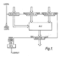
- this shows a portion of a very large scale integrated circuit (VLSI) chip.
- the chip includes an arithmetic and logic unit ALU, having input registers A and B, an output register C, and a control register D which controls the mode of operation of the ALU.
- ALU arithmetic and logic unit
- each of the registers A-D acts as a conventional buffer register with parallel input and output.
- each register can also be operated in a shift mode in which it acts as a shift register, allowing data to be shifted into it by way of a serial data input SDI and shifted out by way of a serial data output SDO.
- the registers A-D are connected in series by means of these serial input and output terminals, to form a serial shift path or loop, extending between a loop data input pin LOOPIN and a loop data output pin LOOPOUT.
- the chip also contains other similar loops (not shown) connected in parallel with the loop shown, by means of a multiplexer MPX which can select the output of any one of the loops for connection to the LOOPOUT pin.
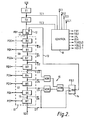
- the register 10 includes eight bit cells BO-B7 arranged in two sections SO, Sl each section containing four cells.
- the cells have respective data inputs PDO-PD7 and data outputs DO-D7 for parallel input and output of data.
- These parallel inputs and outputs are the normal inputs and outputs of the register when it is serving its normal function as part of the data-flow on the chip, and are connected as shown in Figure 1.
- the sections are controlled individually by load enable control signals LECO, LEC1 which enable data to be loaded in parallel into the respective sections SO, S1 from the inputs PDO-PD3 and PD4-PD7.
- Each cell also has a serial data input 11.
- the output of each cell BO-B6 is fed to the serial input 11 of the next cell, so as to connect all the cells BO-B7 together in series as a shift register.
- the output from the last bit cell B7 is connected to the serial data output SDO of the register.
- the register also contains two test control bit cells Tl, T2. These are connected in series between the serial data input SD1 of the register and the serial input 11 of bit cell BO, by way of a multiplexer 12.
- the multiplexer 12 is controlled by a signal FBI.
- FBl When FBl is low, the multiplexer selects the output of bit cell T2. This causes the cells Tl, T2, BO-B7 all to be connected together as a serial shift register between the terminals SD1 and SDO.
- FB1 When FB1 is high, the multiplexer 12 selects a feedback path 13. This path comes from a further multiplexer 14, controlled by a signal FB2.
- the multiplexer 14 selects the output of an exclusive -OR gate tree 15, and when FB2 is high, it selects the output of the last bit cell B7.
- the exclusive -OR gates 15 are connected to the outputs of bit cells B3, B4, B5 and B7 as shown, so as to form the exclusive -OR function (modulo - 2 sum) of these outputs.
- the register has a control circuit 16 which receives the following input signals:
- the control circuit 16 produces the following circuit signals:
- the serial data input 11 of the cell is connected to a NAND gate 21, controlled by the signal ISH.
- the output of this gate is fed to one input of an exclusive -OR gate 22, the other input of which is connected to the output of a NAND gate 23.
- the gate 23 receives the parallel data input PDi for the cell, and is controlled by the signal IPL.
- the output of gate 22 is equal to the data received at the serial input 11.
- the output of gate 22 is equal to the parallel data bit PDi. If both ISH and IPL are high, the output of the gate 22 is the exclusive -OR of the serial and parallel data inputs.
- the output of the gate 23 is connected to one input of a multiplexer 24, the output of which is fed to the data input of a flip-flop (bistable circuit) 25.
- the output of the flip-flop is connected to the other input of the multiplexer 24, and also to the data output Di of the cell.
- the multiplexer 24 is controlled by the signal HOLDn.
- HOLDn When HOLDn is high, the multiplexer selects the output of the flip-flop 25, causing its current contents to be fed back to its input. Thus, the flip-flop is held frozen in its current state, regardless of the condition of its input data signals.
- HOLDn When HOLDn is low, the multiplexer 24 selects the output of the exclusive -OR gate 22, and this allows either the serial input data, the parallel input data, or their exclusive -OR function to be clocked into the flip-flop 25.
- the flip-flop 25 is a master-slave flip-flop controlled by a two-phase clock. Such flip-flops are well known and so it is not necessary to describe it in detail.
- FIG. 4 shows one of the test control bit cells Tl, T2.
- the cell consists of a multiplexer 34 and flip-flop 35 connected in a similar manner to those in Figure"3.
- the multiplexer 34 is controlled by the signal TCHOLD. When TCHOLD is low, the multiplexer selects the serial input path 30 of the cell, allowing data to be shifted serially into the flip-flop 35. When TCHOLD is high, the multiplexer selects the output of the flip-flop, thereby causing the current state of the flip-flop to be frozen.
- the register has seven modes of operation, specified by the control signals DC1, DC2, TC1 and TC2 as follows:
- the signals HOLDO, HOLD1 and TCHOLD are held low, ISH is held high, and IPL is held low.
- data is shifted along the serial shift path through all the cells Tl, T2, BO-B7, between the terminals SDI and SDO.
- This mode can be used to set the test control bit cells Tl, T2 to any desired value, and also to load test data into the bit cells BO-B7 or to read test results from those cells.
- the USER mode is the normal mode of operation, when the register is serving its normal function as a parallel input/output register.
- IPL is held high
- ISH is held low
- the signals HOLDn are controlled directly by the load enable control signals LECn.
- LECn is high
- HOLDn is also high, and this causes the contents of the bit cells in the corresponding section Sn to be frozen.
- LECn is low
- HOLDn is also low, and this allows data to be loaded in parallel into the corresponding section Sn from the data inputs PDO-3 or PD4-7.
- TCHOLD is always held high in this mode and hence the contents of the test control bit cells Tl, T2 are frozen.
- HOLDO, HOLD1 are set low, TCHOLD is high, ISH is high and IPL is low.
- TCHOLD is high
- ISH is high
- IPL is low.
- the register is connected as a circular shift register, allowing its contents to be rotated. This mode is useful for producing sequences of sliding test patterns. For example, if the register is initially loaded with the pattern 0000 0001, the TEST SLIDE mode can be used to rotate this pattern so that the "1" appears successively in each bit position.
- the signals HOLDO, HOLD1 TCHOLD, ISH, IPL, and FB1 all have the same values as in the TEST SLIDE mode. However, in this case, FB2 is held low.
- the multiplexers 12, 14 are therefore now set to select the output of the exclusive -OR gates 15 as the serial input to the bit cell 80.
- the register acts as a feedback shift register, for generating sequences of pseudo-random numbers, for use as test patterns.
- the signals HOLDO, HOLD1, TCHOLD, ISH, FB31 and FB2 are the same as in-the TEST GENERATE mode. However, in this case, IPL is held high.
- the input parallel data PDO-PD7 is combined in the exclusive -OR gates 22 with the shifting data within the register. In this mode, therefore, the register acts as a signature analyser, generating a digital signature from a sequence of parallel inputs. This signature can then be read out, using the SHIFT mode, and used for diagnostic purposes to detect and identify faults in the chip.
- the signal HOLDO is produced by an AND/OR gate combination 40 as shown.
- HOLD1 is produced by a similar logic combination not shown.
- IPL is produced by an AND/OR gate combination 41.
- TCHOLD is produced by an OR gate 42.
- ISH, FBI and FB2 are produced by inverters 43, 44 and 45.
- the TEST SLIDE mode provides the capability for producing circularly shifting test patterns in the register. These patterns are fed by way of the output lines DO-D7 to other circuits on the chip, as test inputs.
- the register BO-B7 may serve as in input register for a PLA, the lines DO-D7 being connected to the bit lines of the array.
- the arithmetic and logic unit ALU may be formed by a PLA, with input registers A, B and D.
- the TEST SLIDE mode can then be used to put a sliding "1" or "0" test pattern on the bit lines so as to enable each bit line individually. This greatly facilitates testing of the PLA.
- the arrangement described above may be modified by including an exclusive -OR gate in the feedback path between the output D7 and the input of the multiplexer 14.
- This gate can be controlled so that it either passes the feedback signal without modification or acts as an inverter. In the latter case, the sliding test pattern is inverted in alternate cycles through the register. This allows further useful sequences of test patterns to be produced.
Abstract
Description
- This invention relates to testing digital integrated circuits.
- One known technique for testing a digital integrated circuit is to provide a pseudo-random number generator integral with the circuit, for producing a sequence of test patterns for applying to the circuit. The pseudo-random number generator may be in the form of a shift register with one or more exclusive -OR gates forming feedback connections from selected stages of the register. The register may double as a normal parallel input/output register forming part of the normal data flow in the integrated circuit. One such arrangement is described, for example, in U.S. Patent No. 3961 252.
- It has been found, however, that pseudo-random generators are not sufficient for testing certain types of circuit, such as programmable logic arrays (PLAs). Such generators either require very long test sequences, or else if a shortened sequence is used certain important test patterns may be omitted, and hence the circuit may not be tested fully.
- An object of the invention is to overcome this problem.
- According to the invention, there is provided a digital integrated circuit including at least one register which is operable in a first mode in which it acts as a parallel input/output register, and in a second mode in which it acts as a pseudo-random number generator for producing test patterns for the circuit, characterised in that the register is also operable in a third mode in which it acts as a circular shift register for producing circularly shifting test patterns.
- It is found that this extra mode, allowing circularly shifting test patterns to be produced, is extremely useful for testing certain types of circuits. For example, when testing a PLA, it can be used to apply a sliding "1" test pattern to the bit lines of the PLA, i.e. to apply a "1" to each bit line in turn, the other lines being held at zero. This allows each bit line to be selected in turn and greatly facilitates systematic checking of the PLA. Other sliding patterns, such as a sliding "0" pattern, are also useful.
- The feedback connection for producing the circular shift may optionally include an inverter, so as to invert the sliding test pattern in alternate cycles through the register. This allows further useful sequences of test patterns to be produced.
- One embodiment of the invention will now be described by way of example with reference to the accompanying drawings.
-
- Figure 1 is a block circuit diagram of a portion of a digital integrated circuit chip in accordance with the invention. Figure 2 is a circuit diagram of a register forming part of the chip.
- Figure 3 is a logic diagram of a bit cell of the register.
- Figure 4 is a logic diagram of a test bit cell associated with the register.
- Figure 5 is a logic diagram of a control circuit associated with the register.
- Referring to Figure 1, this shows a portion of a very large scale integrated circuit (VLSI) chip. The chip includes an arithmetic and logic unit ALU, having input registers A and B, an output register C, and a control register D which controls the mode of operation of the ALU.
- In the normal operation, each of the registers A-D acts as a conventional buffer register with parallel input and output. As will be described, each register can also be operated in a shift mode in which it acts as a shift register, allowing data to be shifted into it by way of a serial data input SDI and shifted out by way of a serial data output SDO. As shown, the registers A-D are connected in series by means of these serial input and output terminals, to form a serial shift path or loop, extending between a loop data input pin LOOPIN and a loop data output pin LOOPOUT. The chip also contains other similar loops (not shown) connected in parallel with the loop shown, by means of a multiplexer MPX which can select the output of any one of the loops for connection to the LOOPOUT pin.
- Referring to Figure 2, this shows one of the registers in more detail. The
register 10 includes eight bit cells BO-B7 arranged in two sections SO, Sl each section containing four cells. The cells have respective data inputs PDO-PD7 and data outputs DO-D7 for parallel input and output of data. These parallel inputs and outputs are the normal inputs and outputs of the register when it is serving its normal function as part of the data-flow on the chip, and are connected as shown in Figure 1. In this normal mode of operation, the sections are controlled individually by load enable control signals LECO, LEC1 which enable data to be loaded in parallel into the respective sections SO, S1 from the inputs PDO-PD3 and PD4-PD7. - Each cell also has a
serial data input 11. The output of each cell BO-B6 is fed to theserial input 11 of the next cell, so as to connect all the cells BO-B7 together in series as a shift register. The output from the last bit cell B7 is connected to the serial data output SDO of the register. The register also contains two test control bit cells Tl, T2. These are connected in series between the serial data input SD1 of the register and theserial input 11 of bit cell BO, by way of amultiplexer 12. - The
multiplexer 12 is controlled by a signal FBI. When FBl is low, the multiplexer selects the output of bit cell T2. This causes the cells Tl, T2, BO-B7 all to be connected together as a serial shift register between the terminals SD1 and SDO. When FB1 is high, themultiplexer 12 selects afeedback path 13. This path comes from afurther multiplexer 14, controlled by a signal FB2. - When FB2 is low, the
multiplexer 14 selects the output of an exclusive -OR gate tree 15, and when FB2 is high, it selects the output of the last bit cell B7. The exclusive -OR gates 15 are connected to the outputs of bit cells B3, B4, B5 and B7 as shown, so as to form the exclusive -OR function (modulo - 2 sum) of these outputs. - The register has a
control circuit 16 which receives the following input signals: - (a) Mode control signals DC1, DC2. These are common to all the registers A-D in the loop.
- (b) Mode control signals TC1, TC2 from the test control bit cells Tl, T2 of the register.
- (c) The load enable control signals LECO, LEC1.
- The
control circuit 16 produces the following circuit signals: - (a) The signals FBI, FB2 which control the
multiplexers - (b) Signals IPL and ISH which are fed in common to all the bit cells BO-B7.
- (c) A signal TCHOLD which is fed to both the test control bit cells Tl, T2.
- (d) Signals HOLDO and HOLD1 which are fed respectively to sections SO and Sl.
- Referring now to Figure 3, this shows one of the bit cells Bi (where i = 0,1---7) in section Sn (where n = 0 or 1).
- The
serial data input 11 of the cell is connected to aNAND gate 21, controlled by the signal ISH. The output of this gate is fed to one input of an exclusive -ORgate 22, the other input of which is connected to the output of aNAND gate 23. Thegate 23 receives the parallel data input PDi for the cell, and is controlled by the signal IPL. - Thus, when ISH is high and IPL is low, the output of
gate 22 is equal to the data received at theserial input 11. When ISH is low and IPL high, the output ofgate 22 is equal to the parallel data bit PDi. If both ISH and IPL are high, the output of thegate 22 is the exclusive -OR of the serial and parallel data inputs. - The output of the
gate 23 is connected to one input of a multiplexer 24, the output of which is fed to the data input of a flip-flop (bistable circuit) 25. The output of the flip-flop is connected to the other input of the multiplexer 24, and also to the data output Di of the cell. - The multiplexer 24 is controlled by the signal HOLDn. When HOLDn is high, the multiplexer selects the output of the flip-
flop 25, causing its current contents to be fed back to its input. Thus, the flip-flop is held frozen in its current state, regardless of the condition of its input data signals. When HOLDn is low, the multiplexer 24 selects the output of the exclusive -OR gate 22, and this allows either the serial input data, the parallel input data, or their exclusive -OR function to be clocked into the flip-flop 25. - The flip-
flop 25 is a master-slave flip-flop controlled by a two-phase clock. Such flip-flops are well known and so it is not necessary to describe it in detail. - Referring now to Figure 4, this shows one of the test control bit cells Tl, T2. The cell consists of a
multiplexer 34 and flip-flop 35 connected in a similar manner to those in Figure"3. Themultiplexer 34 is controlled by the signal TCHOLD. When TCHOLD is low, the multiplexer selects the serial input path 30 of the cell, allowing data to be shifted serially into the flip-flop 35. When TCHOLD is high, the multiplexer selects the output of the flip-flop, thereby causing the current state of the flip-flop to be frozen. - The register has seven modes of operation, specified by the control signals DC1, DC2, TC1 and TC2 as follows:

- In the CHIP HOLD mode, the signals HOLDO, HOLD1, and TCHOLD are held high. Thus, the contents of all the bit cells BO-B7 and both the test control bit cells Tl, T2 are frozen, and cannot be shifted or overwritten.
- In the SHIFT mode, the signals HOLDO, HOLD1 and TCHOLD are held low, ISH is held high, and IPL is held low. Thus, in this mode, data is shifted along the serial shift path through all the cells Tl, T2, BO-B7, between the terminals SDI and SDO. This mode can be used to set the test control bit cells Tl, T2 to any desired value, and also to load test data into the bit cells BO-B7 or to read test results from those cells.
- c The USER mode is the normal mode of operation, when the register is serving its normal function as a parallel input/output register. In this mode, IPL is held high, ISH is held low, and the signals HOLDn are controlled directly by the load enable control signals LECn. Thus, when LECn is high, HOLDn is also high, and this causes the contents of the bit cells in the corresponding section Sn to be frozen. When LECn is low, HOLDn is also low, and this allows data to be loaded in parallel into the corresponding section Sn from the data inputs PDO-3 or PD4-7. TCHOLD is always held high in this mode and hence the contents of the test control bit cells Tl, T2 are frozen.
- In the TEST HOLD mode, the signals HOLDO, HOLD1 and TCHOLD are all held high, so as to freeze the contents of all the bit cells BO-B7, Tl and T2.
- In the TEST SLIDE mode, HOLDO, HOLD1 are set low, TCHOLD is high, ISH is high and IPL is low. This allows data to be shifted serially through the bit cells BO-B7 but not through the test control bit cells Tl, T2. Also, FBI and FB2 are both held high, so that the
multiplexers - In the TEST GENERATE mode, the signals HOLDO, HOLD1 TCHOLD, ISH, IPL, and FB1 all have the same values as in the TEST SLIDE mode. However, in this case, FB2 is held low. The
multiplexers gates 15 as the serial input to the bit cell 80. Hence, in this mode, the register acts as a feedback shift register, for generating sequences of pseudo-random numbers, for use as test patterns. - In the TEST ANALYSE mode, the signals HOLDO, HOLD1, TCHOLD, ISH, FB31 and FB2 are the same as in-the TEST GENERATE mode. However, in this case, IPL is held high. Thus, the input parallel data PDO-PD7 is combined in the exclusive -OR
gates 22 with the shifting data within the register. In this mode, therefore, the register acts as a signature analyser, generating a digital signature from a sequence of parallel inputs. This signature can then be read out, using the SHIFT mode, and used for diagnostic purposes to detect and identify faults in the chip. - Referring now to Figure 5, this shows the
control circuit 16 in detail. - The signal HOLDO is produced by an AND/
OR gate combination 40 as shown. HOLD1 is produced by a similar logic combination not shown. - IPL is produced by an AND/
OR gate combination 41. TCHOLD is produced by anOR gate 42. ISH, FBI and FB2 are produced byinverters - It can be seen that the TEST SLIDE mode provides the capability for producing circularly shifting test patterns in the register. These patterns are fed by way of the output lines DO-D7 to other circuits on the chip, as test inputs. For example, in normal operation the register BO-B7 may serve as in input register for a PLA, the lines DO-D7 being connected to the bit lines of the array. In the circuit shown in Figure 1, for example, the arithmetic and logic unit ALU may be formed by a PLA, with input registers A, B and D. The TEST SLIDE mode can then be used to put a sliding "1" or "0" test pattern on the bit lines so as to enable each bit line individually. This greatly facilitates testing of the PLA.
- The arrangement described above may be modified by including an exclusive -OR gate in the feedback path between the output D7 and the input of the
multiplexer 14. This gate can be controlled so that it either passes the feedback signal without modification or acts as an inverter. In the latter case, the sliding test pattern is inverted in alternate cycles through the register. This allows further useful sequences of test patterns to be produced.
Claims (9)
Applications Claiming Priority (2)
| Application Number | Priority Date | Filing Date | Title |
|---|---|---|---|
| GB858507613A GB8507613D0 (en) | 1985-03-23 | 1985-03-23 | Testing digital integrated circuits |
| GB8507613 | 1985-03-23 |
Publications (2)
| Publication Number | Publication Date |
|---|---|
| EP0196152A2 true EP0196152A2 (en) | 1986-10-01 |
| EP0196152A3 EP0196152A3 (en) | 1989-02-08 |
Family
ID=10576534
Family Applications (1)
| Application Number | Title | Priority Date | Filing Date |
|---|---|---|---|
| EP86300586A Ceased EP0196152A3 (en) | 1985-03-23 | 1986-01-29 | Testing digital integrated circuits |
Country Status (2)
| Country | Link |
|---|---|
| EP (1) | EP0196152A3 (en) |
| GB (1) | GB8507613D0 (en) |
Cited By (6)
| Publication number | Priority date | Publication date | Assignee | Title |
|---|---|---|---|---|
| GB2279783A (en) * | 1993-06-15 | 1995-01-11 | Fujitsu Ltd | Processor having test circuit. |
| EP0656583A1 (en) * | 1993-11-26 | 1995-06-07 | Nec Corporation | Series parallel converter including pseudorandom noise generation |
| GB2383240A (en) * | 2001-12-17 | 2003-06-18 | Micron Technology Inc | DVI link with parallel test data |
| CN1118024C (en) * | 1999-04-05 | 2003-08-13 | 株式会社日立制作所 | Processor with built-in self-checking function |
| US7024601B2 (en) | 2001-12-17 | 2006-04-04 | Micron Technology, Inc. | DVI link with circuit and method for test |
| US7921342B2 (en) * | 2006-02-15 | 2011-04-05 | Stmicroelectronics Sa | Integrated circuit comprising a test mode secured by the use of an identifier, and associated method |
Citations (2)
| Publication number | Priority date | Publication date | Assignee | Title |
|---|---|---|---|---|
| US3961252A (en) * | 1974-12-20 | 1976-06-01 | International Business Machines Corporation | Testing embedded arrays |
| EP0073946A2 (en) * | 1981-09-07 | 1983-03-16 | Siemens Aktiengesellschaft | Method and device for the functional test of a programmed logic device |
-
1985
- 1985-03-23 GB GB858507613A patent/GB8507613D0/en active Pending
-
1986
- 1986-01-29 EP EP86300586A patent/EP0196152A3/en not_active Ceased
Patent Citations (2)
| Publication number | Priority date | Publication date | Assignee | Title |
|---|---|---|---|---|
| US3961252A (en) * | 1974-12-20 | 1976-06-01 | International Business Machines Corporation | Testing embedded arrays |
| EP0073946A2 (en) * | 1981-09-07 | 1983-03-16 | Siemens Aktiengesellschaft | Method and device for the functional test of a programmed logic device |
Non-Patent Citations (2)
| Title |
|---|
| 1979 TEST CONFERENCE, LSI & BOARDS, 23rd-25th October 1979, Cherry Hill, New Jersey, pages 37-41, IEEE; B.K\NEMANN et al.: "Built-in logic block observation techniques" * |
| IEEE TRANSACTIONS ON COMPUTER, vol. C-30, no. 11, November 1981, page 829-833, IEEE, New York, US; W.DAEHN et al.: "A hardware approach to self-testing of large programmable logic arrays" * |
Cited By (15)
| Publication number | Priority date | Publication date | Assignee | Title |
|---|---|---|---|---|
| GB2279783A (en) * | 1993-06-15 | 1995-01-11 | Fujitsu Ltd | Processor having test circuit. |
| US5654972A (en) * | 1993-06-15 | 1997-08-05 | Fujitsu Limited | Processor having test circuit |
| GB2279783B (en) * | 1993-06-15 | 1998-02-25 | Fujitsu Ltd | Processor having test circuit |
| EP0656583A1 (en) * | 1993-11-26 | 1995-06-07 | Nec Corporation | Series parallel converter including pseudorandom noise generation |
| US5506796A (en) * | 1993-11-26 | 1996-04-09 | Nec Corporation | Digital signal processing circuit selectively operable in either a normal or a pseudorandom noise generative mode |
| CN1118024C (en) * | 1999-04-05 | 2003-08-13 | 株式会社日立制作所 | Processor with built-in self-checking function |
| GB2383240A (en) * | 2001-12-17 | 2003-06-18 | Micron Technology Inc | DVI link with parallel test data |
| GB2383240B (en) * | 2001-12-17 | 2005-02-16 | Micron Technology Inc | DVi link with parallel test data |
| US7024601B2 (en) | 2001-12-17 | 2006-04-04 | Micron Technology, Inc. | DVI link with circuit and method for test |
| US7024607B2 (en) | 2001-12-17 | 2006-04-04 | Micron Technology, Inc. | DVI link with parallel test data |
| US7441172B2 (en) | 2001-12-17 | 2008-10-21 | Micron Technology, Inc. | DVI link with parallel test data |
| US7836363B2 (en) | 2001-12-17 | 2010-11-16 | Micron Technology, Inc. | DVI link with circuit and method for test |
| US8024388B2 (en) | 2001-12-17 | 2011-09-20 | Micron Technology, Inc. | DVI link with parallel test data |
| US8321732B2 (en) | 2001-12-17 | 2012-11-27 | Micron Technology, Inc. | DVI link with parallel test data |
| US7921342B2 (en) * | 2006-02-15 | 2011-04-05 | Stmicroelectronics Sa | Integrated circuit comprising a test mode secured by the use of an identifier, and associated method |
Also Published As
| Publication number | Publication date |
|---|---|
| EP0196152A3 (en) | 1989-02-08 |
| GB8507613D0 (en) | 1985-05-01 |
Similar Documents
| Publication | Publication Date | Title |
|---|---|---|
| US4701916A (en) | Digital integrated circuit with multi-mode register | |
| EP0190494B1 (en) | Circuit arrangement for use in an integrated circuit having built in self-test design | |
| US5090035A (en) | Linear feedback shift register | |
| EP0195164B1 (en) | Integrated circuits | |
| US5450415A (en) | Boundary scan cell circuit and boundary scan test circuit | |
| US5412665A (en) | Parallel operation linear feedback shift register | |
| JP2746804B2 (en) | Integrated circuit test method and integrated circuit test apparatus | |
| EP1722246B1 (en) | Method and apparatus for selectively compacting test responses | |
| US5546406A (en) | Cell architecture for built-in self-test of application specific integrated circuits | |
| US4847839A (en) | Digital registers with serial accessed mode control bit | |
| GB2391358A (en) | Method of testing and/or debugging a system on chip (SOC) | |
| JPH03115872A (en) | Test facilitating circuit in digital integrated circuit | |
| US6877119B2 (en) | Circuit scan output arrangement | |
| US4933575A (en) | Electric circuit interchangeable between sequential and combination circuits | |
| US5077740A (en) | Logic circuit having normal input/output data paths disabled when test data is transferred during macrocell testing | |
| KR970003524B1 (en) | Distributed pseudo random sequence control for lsi/vlsi test systems | |
| US6708301B1 (en) | Functional block for integrated circuit, semiconductor integrated circuit, inspection method for semiconductor integrated circuit, and designing method therefor | |
| JP2738351B2 (en) | Semiconductor integrated logic circuit | |
| EP0209982B1 (en) | Digital integrated circuits | |
| US5367551A (en) | Integrated circuit containing scan circuit | |
| EP0196152A2 (en) | Testing digital integrated circuits | |
| US5425034A (en) | Semiconductor integrated logic circuit with internal circuit to be examined by scan path test method | |
| US4730317A (en) | Digital integrated circuits | |
| EP0228156A2 (en) | Test system for VLSI circuits | |
| EP0208393A1 (en) | Testing digital integrated circuits |
Legal Events
| Date | Code | Title | Description |
|---|---|---|---|
| PUAI | Public reference made under article 153(3) epc to a published international application that has entered the european phase |
Free format text: ORIGINAL CODE: 0009012 |
|
| AK | Designated contracting states |
Kind code of ref document: A2 Designated state(s): DE FR GB IT NL |
|
| PUAL | Search report despatched |
Free format text: ORIGINAL CODE: 0009013 |
|
| AK | Designated contracting states |
Kind code of ref document: A3 Designated state(s): DE FR GB IT NL |
|
| 17P | Request for examination filed |
Effective date: 19890123 |
|
| 17Q | First examination report despatched |
Effective date: 19900808 |
|
| STAA | Information on the status of an ep patent application or granted ep patent |
Free format text: STATUS: THE APPLICATION HAS BEEN REFUSED |
|
| 18R | Application refused |
Effective date: 19910211 |
|
| RIN1 | Information on inventor provided before grant (corrected) |
Inventor name: NAVEN, FINBAR Inventor name: HALE, STUART GEORGE |