EP0194783A2 - Uneven-surface data detection apparatus - Google Patents
Uneven-surface data detection apparatus Download PDFInfo
- Publication number
- EP0194783A2 EP0194783A2 EP86301434A EP86301434A EP0194783A2 EP 0194783 A2 EP0194783 A2 EP 0194783A2 EP 86301434 A EP86301434 A EP 86301434A EP 86301434 A EP86301434 A EP 86301434A EP 0194783 A2 EP0194783 A2 EP 0194783A2
- Authority
- EP
- European Patent Office
- Prior art keywords
- light
- uneven
- transparent plate
- hologram
- contact portion
- Prior art date
- Legal status (The legal status is an assumption and is not a legal conclusion. Google has not performed a legal analysis and makes no representation as to the accuracy of the status listed.)
- Granted
Links
Images


Classifications
-
- G—PHYSICS
- G06—COMPUTING; CALCULATING OR COUNTING
- G06V—IMAGE OR VIDEO RECOGNITION OR UNDERSTANDING
- G06V40/00—Recognition of biometric, human-related or animal-related patterns in image or video data
- G06V40/10—Human or animal bodies, e.g. vehicle occupants or pedestrians; Body parts, e.g. hands
- G06V40/12—Fingerprints or palmprints
- G06V40/13—Sensors therefor
- G06V40/1324—Sensors therefor by using geometrical optics, e.g. using prisms
-
- G—PHYSICS
- G06—COMPUTING; CALCULATING OR COUNTING
- G06F—ELECTRIC DIGITAL DATA PROCESSING
- G06F18/00—Pattern recognition
-
- G—PHYSICS
- G02—OPTICS
- G02B—OPTICAL ELEMENTS, SYSTEMS OR APPARATUS
- G02B6/00—Light guides; Structural details of arrangements comprising light guides and other optical elements, e.g. couplings
- G02B6/24—Coupling light guides
- G02B6/26—Optical coupling means
-
- G—PHYSICS
- G06—COMPUTING; CALCULATING OR COUNTING
- G06V—IMAGE OR VIDEO RECOGNITION OR UNDERSTANDING
- G06V40/00—Recognition of biometric, human-related or animal-related patterns in image or video data
- G06V40/40—Spoof detection, e.g. liveness detection
-
- G—PHYSICS
- G07—CHECKING-DEVICES
- G07C—TIME OR ATTENDANCE REGISTERS; REGISTERING OR INDICATING THE WORKING OF MACHINES; GENERATING RANDOM NUMBERS; VOTING OR LOTTERY APPARATUS; ARRANGEMENTS, SYSTEMS OR APPARATUS FOR CHECKING NOT PROVIDED FOR ELSEWHERE
- G07C9/00—Individual registration on entry or exit
- G07C9/30—Individual registration on entry or exit not involving the use of a pass
- G07C9/32—Individual registration on entry or exit not involving the use of a pass in combination with an identity check
- G07C9/37—Individual registration on entry or exit not involving the use of a pass in combination with an identity check using biometric data, e.g. fingerprints, iris scans or voice recognition
-
- G—PHYSICS
- G02—OPTICS
- G02B—OPTICAL ELEMENTS, SYSTEMS OR APPARATUS
- G02B6/00—Light guides; Structural details of arrangements comprising light guides and other optical elements, e.g. couplings
- G02B6/24—Coupling light guides
- G02B6/26—Optical coupling means
- G02B6/35—Optical coupling means having switching means
- G02B6/351—Optical coupling means having switching means involving stationary waveguides with moving interposed optical elements
- G02B6/3522—Optical coupling means having switching means involving stationary waveguides with moving interposed optical elements the optical element enabling or impairing total internal reflection
Definitions
- the present invention relates to an uneven-surface detection apparatus, particularly but not exclusively to such apparatus for detecting fingerprints and the like in a personal identification apparatus.
- a fingerprint is printed on paper using ink and is then sensed using an image sensor.
- a light beam is incident on a glass/air interface at a critical angle or more and an uneven-surface pattern is thus instantaneously obtained.
- a finger surface (uneven-surface pattern having projections (convexes) and recesses (concaves)) is pressed against an oblique side portion of the prism, and illumination light is incident on the oblique side portion thereof at a critical angle or larger.
- the incident light is scattered by projections and is totally reflected by the glass/air interface in recesses, and is then incident on a detector (e.g., an imaging element), thereby allowing detection of the uneven-surface pattern.
- An embodiment of the present invention may allow the provision of a thin, compact uneven-surface data detection apparatus in which contrast of an uneven-surface pattern is improved and a detected image pattern is free from distortion.
- an uneven-surface data detection apparatus comprising at least: a transparent plate having an uneven-surface contact portion against which an uneven surface to be detected is pressed; a light source for illuminating the uneven-surface contact portion through the transparent plate; an uneven-surface image drawing out optical element for drawing out the light reflected on the uneven-surface contact portion from the transparent plate; and a detector for detecting the light drawn out from the transparent plate by the optical element, wherein light reflected by a projection-facing portion of the uneven surface contact portion to be introduced into the detector is diverged from a propagation direction of light reflected by a recess-facing portion of the uneven surface contact portion, and the optical element is arranged to guide the light reflected by the projection-facing portion into the detector.
- FIG. 1- A basic principle of an uneven-surface data detection apparatus according to the present invention will now be described with reference to Fig. 1-
- a human finger 10 1 is pressed against a transparent base 100 (e.g., glass).
- projections (convexes) 102 and recesses (concaves) 103 which constitute a fingerprint of the finger 101, are emphasized.
- the convex 102 is in contact with the glass surface, while the concave 103 is separated away from the glass surface so that an air layer is formed between the concave 103 and the glass surface.
- Light is vertically radiated onto the transparent base 100 from the lower surface side thereof, as indicated by arrows A.
- the light beam which passes through the base 100 and reaches a recess 103 of finger 101 is randomly reflected by the surface of the recess 103, thus being converted into a scattered light beam.
- this scattered light beam enters the base 100 from the upper surface thereof, it is externally emitted from the lower surface of the base 100 at the same angle as its incident angle, in accordance with Snell's law - (as indicated by the tong-dash-short-dash line). Therefore, no scattered light from the recesses 103 is transmitted through the interior of the base 100. In this way, only the totally reflected light transmitted through the interior of the base 100 is detected to obtain an uneven-surface pattern image.
- FIG. 2 is a side view showing the basic principle of the uneven-surface data detection apparatus according to the present invention.
- Reference numeral 1 denotes a transparent plate.
- the plate 1 has an uneven-surface contact portion 1a, against which an uneven surface (e.g., a fingerprint) 5 is pressed.
- a light source 2 for illuminating the uneven surface 5 is arranged below the plate 1.
- an optical element 3 for externally guiding totally reflected light in the plate 1 is disposed, and facing it is a detector 4 for detecting the light guided by the optical element 3.
- the transparent plate 1 need only exhibit transparency with respect to light emitted from the light source used.
- the light components 17 When the light components 17 propagate through the interior of the plate 1 and reach a position corresponding to the optical element 3, since the total reflection condition can be no longer satisfied, the light components 17 enter the optical element 3 through an interface between the plate 1 and the element 3, and are guided externally therefrom. The pattern data from the light components 17 of the projection 9 is then detected by the external detector 4.
- FIGS 3 and 4 are side views of different embodiments of the present invention.
- a transparent plate 1 can be made of either glass or plastic.
- a hologram or a prism which does not satisfy the total reflection condition is preferred.
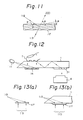
- a hologram 31 is used as an optical element. More specifically, the hologram 31 is mounted on an uneven-surface contact portion 1a of a transparent plate 1 at a position at which it does not interfere with the pressing operation of an uneven surface 5 (e.g. finger thereon. With this arrangement, totally reflected light propagating through the interior of the plate 1 enters the hologram 31, is diffracted thereby and discharged externally, and is then detected by a detector 4.
- an uneven surface 5 e.g. finger thereon.
- Figure 4 illustrates an embodiment wherein a prism 32 is provided instead of the hologram 31.
- the total reflection condition of light components 17 is disturbed by an interface between the prism 32 and the air. Then, the light components 1 7 are diffracted into the prism 32 and are guided externally.
- optical path lengths of the light components propagating through the prism 32 are different, and trapezoidal distortion may occur. If a hologram is used, since all the optical path lengths are the same, trapezoidal distortion cannot occur. Note that if a hologram having a lens function is used, a resultant image can be directly formed on a sensor (e.g., a CCD).
- a sensor e.g., a CCD
- the present invention as described above, all the light components scattered by a recess are discharged outside the transparent plate, and only those scattered by the projection propagate through the interior of the transparent plate. Therefore, only the projection data can be extracted, and as a result, uneven-surface pattern data with a good contrast can be obtained.
- the optical system need comprise only a transparent plate, even when a large uneven surface is to be detected, an increase in the size of the detection apparatus can be prevented.
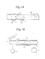
- a residual lipidic or aqueous component (grease or moisture) 26 from a residual fingerprint is attached to the surface of the plate 1 and is in contact with a finger 7, as shown in Fig. 5, it is illuminated with the scattered light from a recess of the finger 7 and acts as a secondary light source.
- the scattered light from the component 26 then propagates through the plate 1 as noise light 27, thus degrading an S/N ratio.
- an uneven-surface data detection apparatus comprises a transparent plate 1 against which an uneven surface 5 to be detected is pressed, a light source 2 for illuminating the uneven surface 5, an optical element 3 for externally guiding light totally reflected through the plate 1 by disturbing the total reflection condition, and an imaging device (detector) 4 for detecting the externally guided light.
- a direction from the surface 5 toward the optical element 3 is given by "-" and a direction opposite thereto is given as " + n, a direction of light for illuminating the uneven surface 5 is set to fall within the range of +33° to -38°.
- Figure 7 shows the apparatus according to this embodiment of the present invention.
- the apparatus of this embodiment comprises the transparent plate 1, the light source 2, the optical element 3 - (e.g., a hologram), and the imaging device 4, as in the embodiment shown in Fig. 3 or 4.
- the main feature of this embodiment is that a light illumination angle of light emitted from the light source 2 with respect to the uneven surface 5 through the plate 1 is set to fall (restricted) within +33° to - 38° if a direction to the right of the surface 5 (i.e., an optical element direction) is given by "-" and a direction opposite thereto is given as " +•.
- Figure 6 is a graph showing the experimentally obtained results of the dependency of the contrast on the illumination angle.
- the illuination angle (of light illuminating the uneven surface from the interior of transparent plate) is plotted along the abscissa, and the contrast of the obtained image data is plotted along the ordinate.
- a curve A indicates a case wherein a fingerprint is detected when the transparent plate is clean
- a curve B indicates a case wherein a fingerpring is detected when a residual fingerprint is left on the transparent plate.
- the illumination angle dependency of the contrast is enhanced.
- the illumination angle range in order to obtain a contrast of 3 or more, the illumination angle range must fall within +33° to -38°.
- an uneven-surface data detection apparatus comprises a transparent plate 1, a light source 2, a hologram 31, and a detector 4.
- this apparatus light components scattered by an uneven object (finger) 7 pressed against the plate 1 are guided directly into the hologram 31, and only projection data, corresponding to light components 116 from a projection 9 of the object 7 which satisfy the Bragg condition of the hologram, is guided into the detector 4.
- Light components from a recess 10 of the object 7 and other light components from the projection 9 not satisfying the Bragg condition are not guided to the detector 4, thus obtaining uneven-surface data from only the projection data.
- a distance between the hologram and an object to be detected is shortened in a hologram reconstruction mode (i.e., in a detection mode)
- aberration due to a difference between the formation wavefront and the reconstruction wavefront of the hologram, and a difference in a height/width ratio of an image can be eliminated.
- Figure 9 is an illustration for explaining this embodiment of the present invention.
- the apparatus of this embodiment comprises a transparent plate 1, a light source 2, a hologram 31, and a detector 4, as in the embodiment shown in Fig. 3.
- the main feature of this embodiment is that in light reflected from a projection 9 of an object (e.g. finger) 7, light components 116 which satisfy the Bragg condition are directly guided into the hologram 31 and are detected by the detector 4.
- Figure 8 shows the relationship between an optical path length, a height/width ratio of a resultant image, and an astigmatic difference- Referring to Fig. 8, the optical path length is plotted along the abscissa, the height/width ratio is plotted along the left ordinate, and the astigmatic difference is plotted along the right ordinate. In addition, a curve A indicates the height/width ratio, and a curve B indicates the astigmatic difference.
- the height/width ratio is a ratio of height and width of longitudinal and lateral focal points of an imaging beam when viewed from a certain point As shown in Fig. 8, as the ratio approaches 1.0, the beam becomes better focused.
- the astigmatic difference is a distance between maximum distortion portions of a beam in both the longitudinal and lateral directions. As the astigmatic difference becomes smaller, aberration can be eliminated and the beam can be better focused.
- the astigmatic difference becomes smaller as the optical path length is shortened.
- Dotted lines in Fig. 8 represent an allowable range of a height/width ratio error.
- the optical path length is preferably set to be 27 mm or less.
- an optical path length is set to be about 17 mm according to the total reflection filtering method of the embodiment shown in Fig. 3, if an effective angle of scattered light from the object is set at 45° and projection data is discriminated from the recess data after total reflection, the thickness of the transparent plate must be set to be about 6 mm, and a detected image overlaps the actual object Therefore, it is (im)possible to obtain an image.
- a clear image with less astigmatic difference can be obtained by a simple method.
- the obtained image has no distortion, no correction means is required and verification can be easily performed, thus providing great practical advantages.
- a hologram 31 is used for drawing out the image data (reflection light) from the transparent plate, if a light source having a wide wavelength band is used, a resultant image may be blurred. Therefore, for example, a laser device whose wavelength range is not wide should preferably be used, thus increasing the total cost.
- a plate-like fingerprint sensor comprises a transparent plate, a light source, an image drawing out hologram, and a detector, and detects a fingerprint in accordance with the total reflection filtering method.
- an LED 11 is used for the light source
- a Lippmann hologram is used for guiding the light from the light source to a finger contact portion.
- the Lippmann hologram is used between the light source and the object (e.g., the finger surface), even if the light source is an LED emitting a range of wavelengths, a certain wavelength can be selected by the wavelength selectivity of a Lippmann hologram, and a clear image can be obtained.
- FIG. 10 shows such an embodiment of the present invention.
- reference numeral 1 denotes a transparent plate; 11, a light source; 31, an image drawing out hologram; 4, a detector; 14, a Lippman hologram; and 7, a finger.
- the Lippmann hologram 14 is formed at an end face of the transparent plate 1, near a portion against which the finger 7 to be detected is pressed, and the LED 11 is arranged at the side of the opposing end face thereof, so that light is incident therefrom.
- the image drawing out hologram 31 and the detector 4 are arranged in the same manner as in the above embodiments.
- light components 216 diffracted by the Lippmann hologram 14 are preferably incident on an air interface 1a of the plate 1, at an angle smaller than the critical angle, so as not to be totally reflected.
- the Lippmann hologram 14 can be formed as shown in Fig.
- a hologram photographic plate 117 is irradiated with a reference wave 118 on the front surface and with an object wave 119 on the back surface thereof.
- Figure 12 shows still another embodiment of the present invention.
- the same reference numerals in Fig. 12 denote the same parts as in Fig. 10.
- an end face of a transparent plate 1 near a finger contact portion is cut obliquely, and a Lippman hologram 14 is formed on the surface opposite to the finger contact portion.
- an LED 11 is arranged so that its light is incident on the obliquely cut end face.
- An image drawing out hologram 31 and a detector 4 are arranged as in the above embodiments.
- the Lippmann hologram 14 used in this embodiment can be prepared as shown in Figs. 13(a) and 13(b), such that a photographic plate 117 is irradiated with a reference wave 118 on the front surface and with an object wave 119 on the back surface thereof.
- the object wave 119 incident from the back surface need not be strictly a parallel beam, but can have a divergence angle which does not exceed a critical angle of the plate 1 in the reconstruction mode, so as not to emit stray light with respect to the read hologram 31.
- an inexpensive LED can be used for the light source, and the total cost of the fingerprint sensor can be reduced, thus providing practical advantages.
- an uneven-surface data detection apparatus comprises a transparent plate 1 against which an uneven surface 5 of an object 7 to be detected is pressed, a light source 2 for illuminating the uneven surface 5, an optical element 3 for externally guiding light which is totally reflected through the interior of the plate 1, and a detector 4 for detecting the externally guided light.
- dust covers 44 and 45 are arranged on air layers on one or both of the upper and lower surfaces of the plate 1.
- Figure 15 shows such an embodiment of the present invention.
- the apparatus of this embodiment comprises the transparent plate 1, the light source 2, the optical element 3 - (e.g., a hologram), and the detector 4, as in the embodiment shown in Fig. 3 or 4.
- the main feature of this embodiment is that dust covers 44 and 45 are arranged on air layers on one or both of the upper and lower surfaces of the transparent plate 1 (in Fig. 15, they are arranged on two surfaces). The dust covers 44 and 45 must be notched at portions corresponding to the upper and lower surfaces of the uneven-surface contact portion and the optical element 3.
- an object to be detected is an embossed pattern or a seal instead of a human finger
- the embossed pattern or seal is generally not flexible, only a portion of a projection thereof will be in tight contact with the transparent plate. when it is pressed thereon. Thus, an air layer is interposed between the other portion of the projection and the transparent plate, and an image thereof becomes blurred.
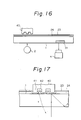
- Figures 16 and 17 show still another embodiment of the present invention, in which Fig. 16 is an illustration showing an arrangement of an uneven-surface date detection apparatus, and Fig. 17 is an illustration for explaining the operation thereof.
- the same reference numerals in Figs. 16 and 17 denote the same parts.
- an uneven-surface data detection apparatus of this embodiment comprising a transparent plate 1, having an elastic film 23 interposed between itself and an object 40, for transmitting light reflected from a projection of the object 40 pressed thereon through the elastic film 23; an optical element 31, for externally guiding light reflected from the projection of the object 40 and propagating through the plate 1; a light source 2 for illuminating the object 40 through the plate 1; and an imaging element (detector) 4 for converting into an electrical signal an optical image guided outside the plate 1 by the optical element 31.
- an air layer interposed between the projection of the object 40 and the transparent plate 1 is filled by the elastic film 23, as shown in Fig. 17.
- an optical image of a rigid pattern in good contrast can be obtained and converted directly into an electrical signal with high precision, just as in the fingerprint sensors in the pre-registered content.
- FIG. 18 is -an illustration showing an arrangement of the apparatus of this embodiment
- Fig. 19 is an illustration for explaining the operation thereof.
- the apparatus of this embodiment comprises the transparent plate 1 having an optical element (e.g., a hologram diffraction grating) 3 1 ; the elastic film 23, made of a very thin rubber and interposed between an object (e.g. , a rigid embossed pattern or a seal) 40 and the transparent plate 1; the light source 2 for illuminating the object 40 through the plate 1; and the imaging element 4 for converting an optical image externally guided by the element 31 into an electrical signal.
- An air layer 2 4 is arranged between the elastic film 23 and the transparent plate 1.
- the apparatus comprises a transparent plate 1 having an optical element (e.g., a hologram diffraction grating) 31; a very thin elastic film 23 interposed between a(rigid)object 40 (e.g. an embossed pattern or a seal) and the plate 1; a light source 2 for illuminating the object 4 0 through the plate 1; and an imaging element 4 for converting into an electrical signal an optical image externally guided by the optical element (hologram) 31-
- the elastic film 23 is formed by a resin (e.g., silicone resin) having a refractive index approximately equal to that of the plate 1, and is in tight contact with the plate 1.
- Figure 20 shows a seat pattern detected by the apparatus of the present invention.
- a seal pattern detected by the apparatus of this embodiment is very clear, as shown in Fig. 20(b), and can be reliably used for personal verification.
- an elastic film is interposed between the rigid object (e.g., the embossed pattern or seal) and the transparent plate, an air layer present between a projection of the object and the transparent plate can be filled with the elastic film.
- an optical image of a rigid pattern having a good contrast can be obtained and converted into a high-precision electrical signal, just as in the fingerprint sensors in Figs. 3 to 15, and can be immediately verified with a pre-registered content
- an uneven-surface data detection apparatus which can reliably detect a rigid object and has a wider application range can be provided.
- Figure 39 is a block diagram showing a proposed personal identification apparatus.
- a fingerprint sensor is used as a personal data input means, as shown in Fig. 39, and the apparatus comprises a fingerprint sensor 6 1 and a data identification dictionary (lexicon) 62. Fingerprint data is registered in advance in the lexicon 62 (e.g., a card) through the sensor 61.
- lexicon e.g., a card
- the input fingerprint is compared with the fingerprint registered in the lexicon 62 by an identification means 63.
- an identification means 63 In such an apparatus, one of the fingerprint sensors in the above embodiments ' could be used as the personal data input means.
- the fingerprint sensor of the above embodiments inputs the electrical signal into the apparatus. Meanwhile, if an input fingerprint coincides with the fingerprint registered in the lexicon 62, the conventional personal identification apparatus determines that a person currently inputting the fingerprint is identical to the registered person.
- the personal identification system can be by-passed.
- the following embodiments relate to a personal identification system and, more particularly, to a personal identification system comprising a bio-detection means and a identification method therefor.
- Figure 22 is a block diagram of a personal identification apparatus according to still another embodiment of the present invention.
- a personal identification apparatus of the present invention as shown in Fig. 22 comprises a bio-detecting means 400, consisting of a photodetecting means 2 4 1 for detecting light in a visible light range having a short wavelength of 44 0 to 580 mm, a photodetecting means 242 for detecting light in a light range having a wavelength longer than 630 nm, a reference voltage generating means 243 for generating a reference voltage in response to the output voltage from the photodetecting means 242, and a comparing means 244 for comparing the reference voltage with the output voltage from the photodetecting means 241.
- bio-detecting means 400 confirms that an object to be detected is a living body
- personal date e.g. fingerprint
- input through a personal data input means 61 and personal data prestored in a data identification lexicon 62 are verified by a data identification means 63.
- human skin has a depression force dependency such that its reflectance varies depending on a depression force in a visible light region of 580 nm of less.
- the output voltage from the photodetecting means 2 4 1 changes before and after a pressure is applied to an object. More specifically, the reference voltage is generated by the reference voltage generating means 243 in response to the output voltage from the photodetecting means 2 4 2, and a change in output voltage from the photodetecting means 241 before and after the application of pressure is detected based on the reference voltage. In this way, it can be detected whether the object is a living body (real finger) or a replica.
- bio-detecting means 4 00 detects that the object is a living body
- personal data input through the personal data input means 61 and personnel data prestored in the data identification lexicon 62 are verified, thereby preventing illegal use of the personal identification system by means of, e.g., a replica of a fingerprint.
- Fig. 23 is a plan view showing a bio-detection optical system according to still another embodiment of the present invention
- Fig. 24 is a circuit diagram of the bio-detecting means.
- a personal data input means (in this embodiment, a fingerprint sensor is used and will be referred to as a fingerprint sensor hereinafter) 6 1 comprises a bio-detection optical system consisting of a means (to be referred to as a short-wavelength photosensor hereinafter) 241 for detecting light of a short wavelength, e.g., 440 to 5 80 nm, and a means (to be referred to as a long-wavelength photosensor hereinafter) 242 for detecting light of a wavelength longer than 630 nm.
- a bio-detection optical system consisting of a means (to be referred to as a short-wavelength photosensor hereinafter) 241 for detecting light of a short wavelength, e.g., 440 to 5 80 nm, and a means (to be referred to as a long-wavelength photosensor hereinafter) 242 for detecting light of a wavelength longer than 630 nm.
- the short-wavelength photosensor 241 has a light-emitting diode 411 and a photodiode 41 2
- the long-wavelength photosensor 242 has a light-emitting diode 421 and a photodiode 422.
- the photosensors 241 and 242 are moved in directions indicated by the arrows, respectively, so as to sandwich a finger 7 placed on the fingerprint sensor 61 therebetween.
- the bio-detecting means 400 comprises a bio-detection optical system consisting of the short-wavelength photosensor 241 and the long-wavelength photosensor 242, a means for generating a reference voltage in response to the output voltage from the photosensor 242, i.e., a reference voltage generator 243, a comparing means for comparing the reference voltage with the output voltage from the photosensor 241, i.e., a bio-discrimination comparator 244, and a contact detection comparator 245 for detecting that the photosensor 242 is brought into contact with the finger 7.
- the bio-detection optical system i.e., the photosensors 241 and 242 are moved in the direction of the arrows, and when the photosensor 242 is brought into contact with the finger 7, a voltage V is generated therefrom.
- a reference voltage V1 input to the comparator 245 is compared with the output voltage V, and when the voltage V exceeds the voltage V1, it is detected that the photosensor 242 is in contact with the finger 7,_ thus setting an terminal of an AND circuit 246 at "1" level.
- An output voltage VO from the photosensor 24 1 is compared with the reference voltage Vr by the comparator 244.
- the comparator 244 detects the above relationship between the output voltage VO from the photosensor 241 and the reference voltage Vr. When the relationship is VO Vr, the comparator 244 generates a discrimination signal, thus setting an ⁇ terminal of the AND circuit 246 at "1" level.
- a flip-flop (FF) 247 is set so that a fingerprint input through the sensor 61 and a fingerprint pre-registered in the data identification lexicon 62 are verified. Note that when the finger is removed from the above bio-detection optical system, the FF 247 is reset because the output level of the comparator 245 is inverted.
- the above relationship is not established between the output voltage VO from the photosensor 241 and the reference voltage Vr, and the discrimination signal is not generated from the comparator 244.
- the bio-detecting means of this embodiment utilizes a depression force dependency unique to human skin such that a reflectance varies widely in the visible light region of 580 nm or less. After the bio-detecting means detects that the object is a living body, a fingerprint input through the fingerprint sensor 61 and a fingerprint pre-registered in the lexicon 62 are verified, thus preventing illegal use of the personal identification system by means of a replica of a fingerprint
- a personal identification system having a function of detecting that an object is a living body can be provided.
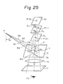
- Figure 25 is a perspective for explaining the causes of such aberrations.
- light scattered at a certain point on a finger is indicated by a single line. In practice, however, the light scattered at a point P propagates to be spread into a diffused spherical waveform before reaching a hologram 31, as shown in Fig. 26(a).
- Figure 25 shows a developed optical path from the point P on the finger to the hologram 31 in Fig. 26(a).
- the light scattered at the point P on the finger passes through points H1 to H5 on the hologram 31, and reaches an eye 75 of an observer through an imaging lens 74. If diffraction light beams 76 are extended in a direction opposite to their propogation direction, they will cross at a point corresponding to an image P(1) of the point P of the finger, which is observed by the observer. However, these beams cannot cross at a signal point, regardless of the position of a screen 77, as indicated by points S1 to S5, thus causing aberration. As described above, since the hologram 31 for guiding data light has a difference between the formation wavefront thereof and the reconstruction wavefront from a fingerprint regardless of object waves, an aberration is generated in a fingerprint image to be detected.
- lattice fringes 3s in the hologram 31 are perpendicular to an optical path extending from the point P to the hologram 31. For this reason, if a direction of the lattice fringes is represented by a vertical direction v, and a direction perpendicular to the fringes is represented by a horizontal direction h aberration can be classified into vertical and horizontal aberrations. Because of the presence of astigmatism, at vertical focal point Pv, shown in Fig. 25, a virtual image P(2) of the point P of the finger is clearly focused in the vertical direction, but is expanded and blurred in the horizontal direction. In contrast to this, at a horizontal focal point Fh, a virtual image P(3) of the point P is focused in the horizontal direction but is expanded and blurred in the vertical direction.
- Figure 27 shows an image on the screen 77 when nine spot-like projections P are pressed against an uneven-surface data input portion 1a. Images P(2) at the vertical focal point Fv are expanded in the horizontal direction to look like horizontal stripes. On the other hand, images P(3) at the horizontal focal point Fh are expanded in the vertical direction to look like vertical stripes.
- the following embodiment of the present invention has as its object to provide an uneven-surface data detection apparatus which is free from the above problems, and can obtain clear uneven-surface data without being adversely influenced by aberration.
- Figure 28 is an illustration for explaining a basic principle of the uneven-surface data detection apparatus of this embodiment.
- Reference numeral 1 denotes a transparent plate having a hologram 31 on its back surface. Assuming that nine spot-like projections P are pressed against an uneven-surface data input portion la of the plate 1, lattice fringes 3s of the hologram 31 are perpendicular to the optical path extending from the portion 1a to the hologram 3 1 . For this reason, virtual images of the projections P in the vertical direction are focused at a vertical focal point Fv near the hologram 31, and those in the horizontal direction are focused at a horizontal focal point Fh further removed from the hologram 31.
- Two orthogonal cylindrical lenses CL1 and CL2 are arranged at positions opposing the hologram 31 of the plate 1.
- the cylindrical lens CL1 nearest the hologram 31 has an axis c parallel to the expansion direction of the virtual images P(3) at the horizontal focal point Fh.
- the cylindrical lens CL2 away from the hologram 31 has an axis parallel to the expansion direction of the virtual images P(2) at the vertical focal point Fv.
- a hologram can provide the same effect as that of a cylindrical lens. Therefore, in this embodiment, all optical elements which have the same function as a cylindrical lens are included in the concept of the cylindrical lens.
- the hologram 31 can be prepared using plane waves for both reference and object waves, or using a spherical wave for at least one of the reference and object waves.
- Figure 29 is an illustration for explaining the operation of the uneven-surface data detection apparatus shown in Fig. 28, in which Fig. 29(a) is a plan view, and Fig. 29(b) is a side view.
- Reference numeral 77 denotes a screen, where two virtual images P(2) and P(3) formed at positions behind the hologram 31 (i.e., at a vertical focal point Fv and a horizonal focal point Fh, respectively) are independently focused on a single screen surface.
- the virtual image P(3) at the horizontal focal point Fh removed from the hologram 31 is focused on the screen 77 by the cylindrical lens CL1 having a focaf length fl.
- the cylindrical lens CL1 since the cylindrical lens CL1 has no convergence function in the axial direction c thereof, the image P(3) is not influenced in the vertical direction.
- the virtual image P(2) at the vertical focal point Fv near the hologram 31 is focused on the screen 77 by the cylindrical lens CL2 having a focal length f2.
- the cylindrical lens CL2 since the cylindrical lens CL2 has no convergence function in the axial direction c thereof, the image P(2) is not influenced in the horizontal direction.
- the problem of the height/width ratio can be solved by properly selecting a difference "f1-f2" of the focal lengths between the two cylindrical lenses CL1 and CL2.
- the image P(4) on the screen 77 can be set at desired lateral and longitudinal magnifications M1 and M2.
- a first cylindrical lens CL1 for correcting a virtual image P-(3) removed from a hologram 31, and a second cylindrical lens CL2 for correcting a virtual image P(2) near the hologram 31 are arranged opposite to the hologram 31 of a transparent plate 1, and are orthogonal to each other.
- two spatial filters SF1 and SF2 are arranged between a position of a screen 77 at which a detecting means is arranged and the cylindrical lenses CL1 and CL2.
- the spatial filters SF1 nearer the cylindrical lenses CL1 and CL2 has a slit S 1 parallel to an axis c of the lens CL1, and the spatial filter SF2 removed from the lenses CL1 and CL2 has a slit S2 parallel to an axis cof the lens CL2.
- Figure 31 is an illustration for explaining a spatial filter function in view of a horizontal focal point correction system, in which Fig. 31 (a) shows a case wherein no spatial fitter is provided, and Fig. 31 (b) shows a case wherein the spatial filter is provided.
- the spatial filter SF1 having the slit S 1 is arranged at the focal point of the cylindrical lens CL1.
- Fig. 31 (a) when no spatial filter SF1 is provided, light incident on the cylindrical lens CL1 from the virtual image P(3) is focused on the screen 77.
- those of light beams 161 which are not parallel to an optical axis 19 of the cylindrical lens CL1 do not pass near the focal point of the lens CL1, image contrast is impaired.
- the spatial filter SF1 having the slit S 1 is arranged at the focal point of the cylindrical lens CL1 as shown in Fig. 31 (b), only light beams 162 substantially parallel to the optical axis 19 can reach the screen 77, but the light beams 161 which cause blurring are cut off by the spatial filter SF1. In this way, even though the light beams 161 which impair the contrast can be cut off, if an optical axis selected by the fitter SF1 coincides with the optical axis of a light beam which satisfies the Bragg condition, decrease in the total amount of light can be avoided.
- an uneven-surface data detection apparatus when characteristic evaluation of the apparatus is performed or a fingerprint is input as personal data, a plurality of specific uneven-surface data are often required. For this purpose, while an uneven surface such as a fingerprint is pressad against an input section, it need only be sensed a plurality of times. However, sensing conditions (e.g., shutter speed) or input conditions of the fingerprint (such as displacement of the finger) may often vary. Therefore, a plurality of uneven-surface data are preferably sensed at the same time.
- sensing conditions e.g., shutter speed
- input conditions of the fingerprint such as displacement of the finger
- FIG 33 is a perspective view for explaining a basic principle of an uneven-surface data detection method according to the present invention.
- Reference numeral 1 denotes a plate having transparency with respect to light emitted from a light source 2.
- the plate 1 has an uneven-surface data input portion 1a on its central front surface.
- a plurality of holograms, e.g., 31 to 34, are arranged on the back surface of the plate 1 to be separated from the center of the input section 1a at equal distances g.
- the holograms 31 to 34 can be either of the phase or surface-relief type.
- a single film 83 for simultaneously sensing images derived from the holograms 31 to 34 are arranged below the plate 1.
- the light source 2 for illuminating the input section 1a is arranged below the back surface of the input section 1a.
- the optical path lengths from the section 1 a to the (identical) holograms 31 to 34 are equal to each other.
- the uneven-surface images can thus be formed on the film 83 under the same conditions.
- the images can be obtained from the holograms 31 to 34 under the same conditions as in an apparatus for obtaining a signal image, the amount of image light will not be small and an exposure time will not be prolonged.
- optical paths extending from the input section 1a a to the holograms 31 to 3 4 are developed, they are the same as those in the previous embodiments. More specifically, diffraction grating fringes 3s are arranged perpendicular to the optical paths extending from the section 1 a to the holograms 31 to 34 and thus are perpendicular to the totally reflected light beams 90.
- Fig. 33 is a view showing the operation principle
- the film 83 is arranged opposite to the transparent plate 1-However, as will be apparent from the following embodiments, light reflected by a reflection mirror can be sensed, or various optical elements can be inserted in the optical paths extending from the holograms 31 to 34 to the imaging film so as to improve characteristics.
- FIG. 34 is a perspective view thereof.
- Holograms 31 to 34 are arranged to be distant from an uneven-surface data input section 1a at equal distances.
- Fig. 34 four holograms are provided, but the number of holograms can be changed in accordance with the number of images obtained at the same time.
- a reflection mirror 84 is obliquely arranged opposite to the surface of the plate 1 on which the holograms 31 to 34 are provided. Therefore, images derived by the holograms 31 to 34 are reflected by the mirror 84.
- Reference numeral 83 denotes a film for sensing the images reflected by the mirror 84.
- a Polaroid camera (trade name) is preferably used for the film 83.
- a plurality of cylindrical lens pairs 151 to 154 are arranged to correspond with the holograms 31 to 34.
- Each of the cylindrical lens pairs 151 to 154 consists of a vertical cylindrical lens CLv and a horizontal cylindrical lens CLh, which are orthogonal to each other. Since a vertical focal point (in a direction of the optical path from the input section 1a to the holograms 31 to 34) does not coincide with a horizontal focal point (in a direction perpendicular to the optical paths) due to astigmatism of the holograms 31 to 34 resultant images are blurred. Therefore, in order to correct the blurred images, the cylindrical lens pairs 151 to 154 are provided.
- a plurality of spatial filter Fv having a slit Sv parallel to the axis of the cylindrical lens CLv and a spatial filter Fh having a slit Sh parallel to the axis of the cylindrical lens CLh are arranged immediately below the respective cylindrical lens pairs 151 to 154.
- a photoetectric conversion element 201 comprising a charge-coupled device is arranged at a position separate from the film 83, so that an image is converted into an electrical signal and is displayed on a display device 202, thus checking if a finger 7 is located at the center of the input section 1 a.
- a direction of the finger 7 in Fig. 34 is reversed.
- a finger image having the same direction as that of the finger on the input section 1 a can be formed on the film 83.
- An odd number of reflection mirrors exceeding 3 can be used-
- the angles of the reflection mirror 84 and the film 83 are selected so that the optical path lengths from the holograms 31 to 34 to the film 83 through the mirror 84 are the same.
- the photoelectric conversion element 201 need only have a size sufficient for detecting an image from any one of the holograms.
- a plurality of holograms 3 1 to 3 4 for drawing out images are arranged at positions separated at equal distances from the input section 1a at the center of the plate 1, and optical images obtained therefrom are formed on a single film, thus obtaining a plurality of uneven-surface data at the same time.
- an exposure time need not be prolonged when compared with a method using a half mirror, and clear images can be obtained with a simple operation.
- total cost can be reduced because of the simple arrangement
- the light source 2 since the light source 2 is arranged immediately below the plate 1, when an operator touches the uneven-surfacce data input section 1a with his finger at the entrance of a computer room, light emitted from the light source 2 may get in his eyes, thus having an adverse influence on his eyes. Since a laser device is normally used for the light source 2, this creates a serious problem.
- a possible solution to this problem is, for example, a tight-shielding cover provided over the apparatus, so that a finger is inserted therein.
- the fingertip cannot be precisely aligned with the center of the input section 1a.
- the input section 1a is easily contaminated with an aqueous or lipidic component of a residual fingerprint, the light cover makes it difficult to see the contaminated portion and clean it
- a touch switch for detecting the contacting of a finger is provided on transparent plate 1, so that only when it is detected that the finger is being pressed against the input section 1a, is the laser light source 2 enabled.
- a special control circuit is then required, and light leaking around the finger may also undesirably get in the operator's eyes.
- FIG. 38 shows a method of detecting uneven-surface data under totally, reflected illumination, in which the concept of the transparent plate 1 is also adopted.
- the end face of a transparent plate 1 is obliquely cut, so that a laser beam 86 becomes incident from an oblique surface 85.
- the laser beam is totally reflected at regions between a-a' and b-b', in which the laser beam 86 is reflected by a transparent plate/air interface on the surface of the plate 1, thus enabling totally reflected illumination.
- Fig. 38(b) when an angle a of the oblique surface 85 and a critical angle 2of the transparent plate surface are selected, total reflection is repeated, and totally reflected light 87 is guided to a hologram 31 without exiting in the plate 1.
- the regions between a-a' and b-b' of the front surface of the plate 1 are used as the uneven-surface data input section la, light is scattered by a projection 9 of the uneven surface, and propagates to the hologram 31 just as in the case shown in Fig. 17.
- the totally reflected light also reaches the hologram 3 1 .
- the projection 9 is dark and the recess 10 is bright, like a negative film.
- an incident angle i to the hologram 31 is set at an angle different from the critical angle c, the totally reflected light 87 is not incident on the hologram 31, and only the scattered light from the projection 9 is incident thereon.
- the following embodiment of the present invention aims to provide an uneven-surface data detection apparatus with the above arrangement, which is free from the above problem and which can detect high-contrast uneven-surface data without being influenced by the totally reflected light.
- Figure 35 is an illustration for explaining a basic principle of an uneven-surface data detection apparatus according to this embodiment, in which Fig. 35(a) is a plan view and Fig. 35(b) is a sectional view taken along a line b-b' of Fig. 35(a).
- Reference numeral 1 denotes a plate having transparency with respect to light emitted from a light source 2.
- An uneven-surface data input section 1 a is illuminated by totally reflected light 87.
- the input section 1a is arranged on the front surface of the plate 1 midway along an optical path of totally reflected light 87.
- Reference numeral 3 1 denotes a hologram for guiding an optical image outside the plate 1.
- the hologram 31 is arranged at a position away from the optical path of the light 87.
- An optical image externally guided by the hologram 31 is detected by an imaging element (detector) 4.
- the end face of the plate 1 is cut obliquely, so that a laser beam becomes incident through an oblique surface 85 thereof.
- another hologram is provided on the back surface of the transparent plate 1, and is irradiated with a laser beam so as to introduce the beam into the plate 1.
- the light 87 illuminates the uneven surface thereof and then propagates to be repetitively totally reflected.
- light scattered by a projection 9 of the finger 7 radially propagates in every direction, as indicated by numeral 17 in Fig. 35(a).
- the light 87 is not transmitted to the image position of the hologram 31 to be incident on the hologram 31 and to brighten the image, thus preventing a poor-contrast image. Since the light 87 is only totally reflected in the plate 1, it can no longer get in eyes of an operator when he touches the input section 1 a.
- Fig. 36 is a perspective view of an uneven-surface data detection apparatus of this embodiment. Since a transparent plate 1 has an L-shape, when a laser beam from a light source 2 becomes incident through an oblique surface 85 of the end portion of the plate 1, light 87 propagates in the plate 1 and is totally reflected. Light scattered by a projection of an uneven surface is totally reflected toward a hologram 31 arranged on the back surface of the end of the L-shaped portion opposite the light source 2, is guided outside the plate 1, and is then detected by an imaging element 4. Alternatively, if the hologram 31 is arranged at a position away from the optical path of the light 87, the plate 1 can be formed into a desired shape.
- Figure 37 shows an improvement in the apparatus of the embodiment in Fig. 36.
- An image obtained from the hologram 31 is reflected by a reflection mirror 620, and becomes incident on the imaging element 4 through a cylindrical lens pair 621 and a spatial filter pair 622.
- the cylindrical lenses 621 and the spatial filters 622 can be arranged immediately below the hologram 31 without using the mirror 620.
- the cylindrical lens pair 621 consists of a vertical cylindrical lens CLv and a horizontal cylindrical lens CLh, which are orthogonal to each other.
- a vertical focal point (in a direction of optical path from the input section 1a to the hologram 31) does not coincide with a horizontal focal point (in a direction perpendicular to the optical path) due to astigmatism of the hologram 31, and a resultant image is blurred.
- the cylindrical lenses CLv and CLh are provided.
- the spatial filter pair 622 consists of a spatial filter Fv having a slit Sv parallel to the axis of the cylindrical lens CLv and a spatial filter Fh having a slit Sh parallel to the axis of the cylindrical lens CLh.
- the uneven-surface data detection apparatus in which the uneven-surface data input section 1 a is illuminated with totally reflected light so as to protect the eyes of an operator from a laser beam, since the hologram 31 is arranged at a position away from the optical path of the totally reflected light, the totally reflected light will not reach the hologram 3 1 . As a result, the problem of part of the totally reflected light reaching the hologram 31 to result in a poor-contrast image is solved.
Abstract
Description
- The present invention relates to an uneven-surface detection apparatus, particularly but not exclusively to such apparatus for detecting fingerprints and the like in a personal identification apparatus.
- In the high-tech information world of today, a strong demand has recently arisen for better computer system security techniques. In particular, in order to protect data confidentiality a reliable identification must be made of personnel in charge of such systems, and thus strict checks on entrance to a computer room have become very important. In the past, passwords and ID cards have been used and now personal identification systems using fingerprints are in increasing use.
- In a conventional method for inputting uneven-surface data (e.g., fingerprint), a fingerprint is printed on paper using ink and is then sensed using an image sensor. In another method, a light beam is incident on a glass/air interface at a critical angle or more and an uneven-surface pattern is thus instantaneously obtained.
- In the former method, a finger must be stained with ink each time the fingerprint data is to be input, and an uneven coating or blurring of the ink makes the input operation difficult.
- In a proposed uneven-surface data detection apparatus using a prism, a finger surface (uneven-surface pattern having projections (convexes) and recesses (concaves)) is pressed against an oblique side portion of the prism, and illumination light is incident on the oblique side portion thereof at a critical angle or larger. The incident light is scattered by projections and is totally reflected by the glass/air interface in recesses, and is then incident on a detector (e.g., an imaging element), thereby allowing detection of the uneven-surface pattern.
- However, light leaks through the unclean oblique surface due to remaining fingerprints or moisture, and this light leakage irradiates the concave portion of the fingerprint and is scattered. Therefore, the level of signal light from the convex portion is lowered, thus degrading the contrast of the uneven-surface pattern. Since a prism is used, the total thickness of the apparatus cannot be reduced. More specifically, if the uneven-surface pattern of the entire palm is to be detected, a large prism must be used, resulting in a bulky apparatus. In addition, the resultant image may be distorted to a trapezoid shape due to a difference in optical path length from the surface of the palm to the detector.
- An embodiment of the present invention may allow the provision of a thin, compact uneven-surface data detection apparatus in which contrast of an uneven-surface pattern is improved and a detected image pattern is free from distortion.
- According to the present invention, there is provided an uneven-surface data detection apparatus, comprising at least: a transparent plate having an uneven-surface contact portion against which an uneven surface to be detected is pressed; a light source for illuminating the uneven-surface contact portion through the transparent plate; an uneven-surface image drawing out optical element for drawing out the light reflected on the uneven-surface contact portion from the transparent plate; and a detector for detecting the light drawn out from the transparent plate by the optical element, wherein light reflected by a projection-facing portion of the uneven surface contact portion to be introduced into the detector is diverged from a propagation direction of light reflected by a recess-facing portion of the uneven surface contact portion, and the optical element is arranged to guide the light reflected by the projection-facing portion into the detector.
- Reference is made, by way of example, to the accompanying drawings in which:
- Figure 1 is an illustration for explaining a principle of the present invention;
- Fig. 2 is a side view showing an uneven-surface data detection apparatus according to a basic principle of the present invention;
- Fig. 3 is a side view showing an embodiment of the present invention;
- Fig. 4 is a side view showing another embodiment of the present invention;
- Fig. 5 is an illustration for explaining the influence of a residual lipidic component on a transparent base;
- Fig. 6 is a graph showing the dependency of contrast on an illumination angle;
- Fig. 7 is an illustration showing an arrangement of still another embodiment of the present invention;
- Fig. 8 is a graph showing the relationship between an optical path length, a height/width ratio of an obtained image, and an astigmatic difference;
- Fig.9 is an illustration showing an arrangement according to still another embodiment of the present invention;
- Fig. 10 is an illustration showing an arrangement according to still another embodiment of the present invention;
- Fig. 11 is an illustration for explaining a method of preparing a hologram in the embodiment shown in Fig. 10;
- Fig. 12 is an illustration showing an arrangement according to still another embodiment of the present invention;
- Fig. 13 is an illustration for explaining a method of preparing a hologram in the embodiment shown in Fig. 12;
- Fig. 14 is an illustration for explaining the influence of a residual lipidic component on a transparent base;
- Fig. 15 is an illustration showing an arrangement according to still another embodiment of the present invention;
- Fig. 16 is an illustration showing an arrangement according to still another embodiment of the present invention;
- Fig. 17 is an illustration for explaining the operation of the embodiment shown in Fig. 16;
- Fig. 18 is an illustration showing an arrangement according to still another embodiment of the present invention;
- Fig. 19 is an illustration for explaining the operation of the embodiment shown in Fig. 18;
- Fig. 20 is an illustration for explaining a detected seal pattern;
- Fig. 21 is a graph showing a spectral reflectance of human skin;
- Fig. 22 is a block diagram showing a persona! identification apparatus according to the present invention;
- Fig. 23 is a plan view of a bio-detection optical system for the apparatus shown in Fig. 22;
- Fig. 24 is a circuit diagram of a bio-detection means in Fig. 23;
- Fig. 25 is an illustration for explaining causes of aberrations in a hologram;
- Fig. 26 is an illustration for explaining a method of preparing a hologram and of reconstructing an image in an uneven-surface data detection apparatus embodying the present invention;
- Fig. 27 is an illustration for explaining causes of aberrations in the uneven-surfacce detection apparatus;
- Fig. 28 is an illustration showing an arrangement according to still another embodiment of the present invention;
- Fig. 29 is an illustration for explaining the operation of the embodiment shown in Fig. 28;
- Fig. 30 is an illustration showing an arrangement according to still another embodiment of the present invention;
- Fig. 31 is an illustration for explaining the operation of the embodiment shown in Fig. 30;
- Fig. 32 is a plan view showing an optical path from an uneven-surface data input section;
- Fig. 33 is an illustration for explaining a principle of still another embodiment of the present invention;
- Fig. 34 is an illustration showing an arrangement of the embodiment shown in Fig. 33;
- Fig. 35 is an illustration for explaining a principle of still another embodiment of the present invention;
- Fig. 36 is an illustration showing an arrangement according to still another embodiment of the present invention;
- Fig. 37 is an illustration showing an embodiment improved over the embodiment of Fig. 36;
- Fig. 38 is an illustration for explaining a laser optical path of an uneven-surface data detection apparatus embodying the present invention; and
- Fig. 39 is a block diagram of a proposed personal identification system.
- A basic principle of an uneven-surface data detection apparatus according to the present invention will now be described with reference to Fig. 1- A
human finger 101 is pressed against a transparent base 100 (e.g., glass). In Fig. 1, projections (convexes) 102 and recesses (concaves) 103, which constitute a fingerprint of thefinger 101, are emphasized. As can be seen from the drawing, theconvex 102 is in contact with the glass surface, while the concave 103 is separated away from the glass surface so that an air layer is formed between the concave 103 and the glass surface. Light is vertically radiated onto thetransparent base 100 from the lower surface side thereof, as indicated by arrows A. Light entering the interior of thebase 100 is randomly reflected by theprojections 102, and is thereby scattered in all directions, since no air layer is formed at the convex portion. Scattered light beams which satisfy the total reflection condition of the base 100 (i.e., have an angle larger than a critical angle) are totally reflected by the lower surface of thebase 100, as indicated by the dashed line in Fig. 1, and are then totally reflected by the upper surface thereof (although not illustrated in Fig. 1), thus being transmitted through the interior of thebase 100. On the other hand, light passes through thebase 100 at theconcave portion 103, since an air layer is formed at this portion. The light beam which passes through thebase 100 and reaches arecess 103 offinger 101 is randomly reflected by the surface of therecess 103, thus being converted into a scattered light beam. When this scattered light beam enters thebase 100 from the upper surface thereof, it is externally emitted from the lower surface of thebase 100 at the same angle as its incident angle, in accordance with Snell's law - (as indicated by the tong-dash-short-dash line). Therefore, no scattered light from therecesses 103 is transmitted through the interior of thebase 100. In this way, only the totally reflected light transmitted through the interior of thebase 100 is detected to obtain an uneven-surface pattern image. - Figure 2 is a side view showing the basic principle of the uneven-surface data detection apparatus according to the present invention.
Reference numeral 1 denotes a transparent plate. Theplate 1 has an uneven-surface contact portion 1a, against which an uneven surface (e.g., a fingerprint) 5 is pressed. Alight source 2 for illuminating theuneven surface 5 is arranged below theplate 1. At the other end of theportion 1a, anoptical element 3 for externally guiding totally reflected light in theplate 1 is disposed, and facing it is adetector 4 for detecting the light guided by theoptical element 3. - It should be noted that the
transparent plate 1 need only exhibit transparency with respect to light emitted from the light source used. - When the
uneven surface 5 is pressed against thetransparent plate 1 and is illuminated with thelight source 2, light components reflected by aprojection 9 and those reflected by arecess 10 of theuneven surface 5 propagate in different directions, respectively. More specifically,light components 16 scattered by therecess 10 enter theplate 1, are refracted, and are then discharged outside theplate 1. On the other hand,light components 17 scattered by theprojection 9 and having an angle larger than a critical angle are totally, repetitively reflected at transparent plate/air interfaces and propagate through the interior of the plate 1 - (note, otherlight components 17 having an angle less than the critical angle are discharged outside the plate 1). The convex data and the concave data are discriminated depending on whether or not the air layer is formed between the plate and the finger. Since all thelight components 16 scattered by therecess 10 are discharged outside theplate 1, thelight components 17 propagating through the interior of theplate 1 correspond to data from theprojection 9 and need be detected only to obtain uneven-surface pattern data with a good contrast. - When the
light components 17 propagate through the interior of theplate 1 and reach a position corresponding to theoptical element 3, since the total reflection condition can be no longer satisfied, thelight components 17 enter theoptical element 3 through an interface between theplate 1 and theelement 3, and are guided externally therefrom. The pattern data from thelight components 17 of theprojection 9 is then detected by theexternal detector 4. - An application of the uneven-surface data detection apparatus of this invention will now be described. Figures 3 and 4 are side views of different embodiments of the present invention. A
transparent plate 1 can be made of either glass or plastic. In order to guide the totally reflected light through the interior of theplate 1 externally, a hologram or a prism which does not satisfy the total reflection condition is preferred. - In Fig. 3, a
hologram 31 is used as an optical element. More specifically, thehologram 31 is mounted on an uneven-surface contact portion 1a of atransparent plate 1 at a position at which it does not interfere with the pressing operation of an uneven surface 5 (e.g. finger thereon. With this arrangement, totally reflected light propagating through the interior of theplate 1 enters thehologram 31, is diffracted thereby and discharged externally, and is then detected by adetector 4. - Figure 4 illustrates an embodiment wherein a
prism 32 is provided instead of thehologram 31. The total reflection condition oflight components 17 is disturbed by an interface between theprism 32 and the air. Then, thelight components 17 are diffracted into theprism 32 and are guided externally. In this embodiment, however, optical path lengths of the light components propagating through theprism 32 are different, and trapezoidal distortion may occur. If a hologram is used, since all the optical path lengths are the same, trapezoidal distortion cannot occur. Note that if a hologram having a lens function is used, a resultant image can be directly formed on a sensor (e.g., a CCD). - According to the present invention as described above, all the light components scattered by a recess are discharged outside the transparent plate, and only those scattered by the projection propagate through the interior of the transparent plate. Therefore, only the projection data can be extracted, and as a result, uneven-surface pattern data with a good contrast can be obtained. In particular, since the optical system need comprise only a transparent plate, even when a large uneven surface is to be detected, an increase in the size of the detection apparatus can be prevented.
- In the above-mentioned apparatus, when a residual lipidic or aqueous component (grease or moisture) 26 from a residual fingerprint is attached to the surface of the
plate 1 and is in contact with afinger 7, as shown in Fig. 5, it is illuminated with the scattered light from a recess of thefinger 7 and acts as a secondary light source. The scattered light from thecomponent 26 then propagates through theplate 1 asnoise light 27, thus degrading an S/N ratio. - For this reason, according to another embodiment of the present invention shown in Fig. 7, an uneven-surface data detection apparatus comprises a
transparent plate 1 against which anuneven surface 5 to be detected is pressed, alight source 2 for illuminating theuneven surface 5, anoptical element 3 for externally guiding light totally reflected through theplate 1 by disturbing the total reflection condition, and an imaging device (detector) 4 for detecting the externally guided light. In this apparatus, assume that when a direction from thesurface 5 toward theoptical element 3 is given by "-" and a direction opposite thereto is given as " + n, a direction of light for illuminating theuneven surface 5 is set to fall within the range of +33° to -38°. - Since a light illumination angle with respect to the
surface 5 falls within the range of +33° to -38°, an amount of light which is reflected from a recess of thesurface 5 and propagates toward theoptical element 3 can be reduced, as explained below, and an influence due to a residual fingerprint can be eliminated, thus preventing degradation in the S/N ratio. - Figure 7 shows the apparatus according to this embodiment of the present invention.
- The apparatus of this embodiment comprises the
transparent plate 1, thelight source 2, the optical element 3 - (e.g., a hologram), and theimaging device 4, as in the embodiment shown in Fig. 3 or 4. The main feature of this embodiment is that a light illumination angle of light emitted from thelight source 2 with respect to theuneven surface 5 through theplate 1 is set to fall (restricted) within +33° to - 38° if a direction to the right of the surface 5 (i.e., an optical element direction) is given by "-" and a direction opposite thereto is given as " +•. - Figure 6 is a graph showing the experimentally obtained results of the dependency of the contrast on the illumination angle. Referring to Fig. 6, the illuination angle (of light illuminating the uneven surface from the interior of transparent plate) is plotted along the abscissa, and the contrast of the obtained image data is plotted along the ordinate. In addition, a curve A indicates a case wherein a fingerprint is detected when the transparent plate is clean, and a curve B indicates a case wherein a fingerpring is detected when a residual fingerprint is left on the transparent plate. As can be seen from Fig. 6, when the residual fingerprint remains, the illumination angle dependency of the contrast is enhanced. In this case, in order to obtain a contrast of 3 or more, the illumination angle range must fall within +33° to -38°.
- In this embodiment, even if a lipidic or aqueous component becomes attached to the transparent plate, a good contrast can be obtained. Note that, in the apparatus of Fig. 3 or 4, if the influence of a residual fingerprint is present, a load may be applied to a verification algorithm and a verification rate may be degraded. However, such problems are obviated in the above-mentioned embodiment.
- According to the apparatus of this embodiment as above, even if a lipidic or aqueous component caused by a residual fingerprint becomes attached to the transparent plate, a high contrast image can be obtained, thus providing great practical advantages.
- In the uneven-surface data detection method of Fig. 3 or 4, astigmatism caused by a difference between a formation wavefront and a reconstruction wavefront of a hologram can be generated, thus blurring the image.
- For this reason, in another embodiment of the present invention shown in Fig. 9, an uneven-surface data detection apparatus comprises a
transparent plate 1, alight source 2, ahologram 31, and adetector 4. In. this apparatus, light components scattered by an uneven object (finger) 7 pressed against theplate 1 are guided directly into thehologram 31, and only projection data, corresponding tolight components 116 from aprojection 9 of theobject 7 which satisfy the Bragg condition of the hologram, is guided into thedetector 4. Light components from arecess 10 of theobject 7 and other light components from theprojection 9 not satisfying the Bragg condition are not guided to thedetector 4, thus obtaining uneven-surface data from only the projection data. - When a distance between the hologram and an object to be detected is shortened in a hologram reconstruction mode (i.e., in a detection mode), aberration due to a difference between the formation wavefront and the reconstruction wavefront of the hologram, and a difference in a height/width ratio of an image, can be eliminated.
- Figure 9 is an illustration for explaining this embodiment of the present invention.
- The apparatus of this embodiment comprises a
transparent plate 1, alight source 2, ahologram 31, and adetector 4, as in the embodiment shown in Fig. 3. The main feature of this embodiment is that in light reflected from aprojection 9 of an object (e.g. finger) 7,light components 116 which satisfy the Bragg condition are directly guided into thehologram 31 and are detected by thedetector 4. - Figure 8 shows the relationship between an optical path length, a height/width ratio of a resultant image, and an astigmatic difference- Referring to Fig. 8, the optical path length is plotted along the abscissa, the height/width ratio is plotted along the left ordinate, and the astigmatic difference is plotted along the right ordinate. In addition, a curve A indicates the height/width ratio, and a curve B indicates the astigmatic difference.
- Note that the height/width ratio is a ratio of height and width of longitudinal and lateral focal points of an imaging beam when viewed from a certain point As shown in Fig. 8, as the ratio approaches 1.0, the beam becomes better focused. The astigmatic difference is a distance between maximum distortion portions of a beam in both the longitudinal and lateral directions. As the astigmatic difference becomes smaller, aberration can be eliminated and the beam can be better focused.
- As can be seen from Fig. 8, the astigmatic difference becomes smaller as the optical path length is shortened. Dotted lines in Fig. 8 represent an allowable range of a height/width ratio error. When the allowable range is 5%, the optical path length is preferably set to be 27 mm or less.
- With the arrangement satisfying this condition shown in Fig. 9,
light components 116 which are reflected from theprojection 9 of theobject 7 and satisfy the Bragg condition are diffracted by thehologram 31, and reach thedetector 4, as indicated by a. However, almost all of thelight components 116 from therecess 10 cannot satisfy the Bragg condition, and are discharged into an air layer on the basis of Snell's law, as indicated by b. Although thecomponents 116 are partially diffracted, as indicated by c, since they are weak and do not satisfy the Bragg condition, they propagate in a different direction. Therefore, essentially only the projection data light is detected and a fingerprint image is obtained. - When an optical path length is set to be about 17 mm according to the total reflection filtering method of the embodiment shown in Fig. 3, if an effective angle of scattered light from the object is set at 45° and projection data is discriminated from the recess data after total reflection, the thickness of the transparent plate must be set to be about 6 mm, and a detected image overlaps the actual object Therefore, it is (im)possible to obtain an image.
- According to the embodiment described above, a clear image with less astigmatic difference can be obtained by a simple method. In addition, since the obtained image has no distortion, no correction means is required and verification can be easily performed, thus providing great practical advantages.
- In the embodiment of Fig. 3, since the
hologram 31 is used for drawing out the image data (reflection light) from the transparent plate, if a light source having a wide wavelength band is used, a resultant image may be blurred. Therefore, for example, a laser device whose wavelength range is not wide should preferably be used, thus increasing the total cost. - For this reason, according to still another embodiment of the present invention, as shown in Fig. 10, a plate-like fingerprint sensor comprises a transparent plate, a light source, an image drawing out hologram, and a detector, and detects a fingerprint in accordance with the total reflection filtering method. In this apparatus, an
LED 11 is used for the light source, and a Lippmann hologram is used for guiding the light from the light source to a finger contact portion. - Since the Lippmann hologram is used between the light source and the object (e.g., the finger surface), even if the light source is an LED emitting a range of wavelengths, a certain wavelength can be selected by the wavelength selectivity of a Lippmann hologram, and a clear image can be obtained.
- Fig. 10 shows such an embodiment of the present invention. In Figure 10,
reference numeral 1 denotes a transparent plate; 11, a light source; 31, an image drawing out hologram; 4, a detector; 14, a Lippman hologram; and 7, a finger. - In this embodiment, as shown in Fig. 10, the
Lippmann hologram 14 is formed at an end face of thetransparent plate 1, near a portion against which thefinger 7 to be detected is pressed, and theLED 11 is arranged at the side of the opposing end face thereof, so that light is incident therefrom. The image drawing outhologram 31 and thedetector 4 are arranged in the same manner as in the above embodiments. Note thatlight components 216 diffracted by theLippmann hologram 14 are preferably incident on anair interface 1a of theplate 1, at an angle smaller than the critical angle, so as not to be totally reflected. The Lippmann hologram 14 can be formed as shown in Fig. 11, such that a hologramphotographic plate 117 is irradiated with areference wave 118 on the front surface and with anobject wave 119 on the back surface thereof. When a reconstruction wave is radiated from the direction of thereference wave 118, areflection wave 200 is emitted in a direction which satisfies a relationship λ = 2Psinφ (where λ is a wavelength, P is a pitch of interference fringes, and is an angle of incident light with respect to the fringes). - With this arrangement, light from the
LED 11 having a wide wavelength band is filtered to have a certain wavelength by the wavelength selectivity of theLippmann hologram 14, and is then detected by thedetector 4, thus obtaining a clear fingerprint image. Note that the operation of this embodiment is the same as the above embodiments, and a detailed description thereof is omitted. - Figure 12 shows still another embodiment of the present invention. The same reference numerals in Fig. 12 denote the same parts as in Fig. 10.
- In this embodiment, an end face of a
transparent plate 1 near a finger contact portion is cut obliquely, and aLippman hologram 14 is formed on the surface opposite to the finger contact portion. In addition, anLED 11 is arranged so that its light is incident on the obliquely cut end face. An image drawing outhologram 31 and adetector 4 are arranged as in the above embodiments. The Lippmann hologram 14 used in this embodiment can be prepared as shown in Figs. 13(a) and 13(b), such that aphotographic plate 117 is irradiated with areference wave 118 on the front surface and with anobject wave 119 on the back surface thereof. In this case, theobject wave 119 incident from the back surface need not be strictly a parallel beam, but can have a divergence angle which does not exceed a critical angle of theplate 1 in the reconstruction mode, so as not to emit stray light with respect to the readhologram 31. - The operation and effect of this embodiment is the same as the embodiment of Fig. 10.
- According to the present invention as described above, an inexpensive LED can be used for the light source, and the total cost of the fingerprint sensor can be reduced, thus providing practical advantages.
- In the apparatus shown in Fig. 3 or 4, when a lipidic or
aqueous component 26 from a finger becomes attached to thetransparent plate 1, as shown in Fig. 14,optical noise 29 is increased thereby, and signal light 17 is reduced, thus degrading the S/N ratio. - For this reason, according to still another embodiment of the present invention as shown in Fig. 15, an uneven-surface data detection apparatus comprises a
transparent plate 1 against which anuneven surface 5 of anobject 7 to be detected is pressed, alight source 2 for illuminating theuneven surface 5, anoptical element 3 for externally guiding light which is totally reflected through the interior of theplate 1, and adetector 4 for detecting the externally guided light. In this apparatus, dust covers 44 and 45 are arranged on air layers on one or both of the upper and lower surfaces of theplate 1. - Since the dust covers 44 and 45 are provided on the transparent plate through the air layer, a lipidic or aqueous component cannot become attached to the transparent plate, thus preventing the S/N ratio from being impaired.
- Figure 15 shows such an embodiment of the present invention.
- The apparatus of this embodiment comprises the
transparent plate 1, thelight source 2, the optical element 3 - (e.g., a hologram), and thedetector 4, as in the embodiment shown in Fig. 3 or 4. The main feature of this embodiment is that dust covers 44 and 45 are arranged on air layers on one or both of the upper and lower surfaces of the transparent plate 1 (in Fig. 15, they are arranged on two surfaces). The dust covers 44 and 45 must be notched at portions corresponding to the upper and lower surfaces of the uneven-surface contact portion and theoptical element 3. - With the above arrangement, attachment of a lipidic or aqueous component on the greater part of the
transparent plate 1 can be prevented by the dust covers 44 and 45. Therefore, degradation in the S/N ratio due to attachment of the lipidic or aqueous component can be prevented. Since the air layers are sandwiched between the dust covers 44 and 45 and thetransparent plate 1, the dust covers 44 and 45 will not adversely influence the total reflection condition of light propagating through the interior of thetransparent plate 1. - According to the present invention as described above, degradation in the S/N ratio of the apparatus can be reduced or prevented by a very simple arrangement, and is effective for practical use.
- In the above embodiments, when an object to be detected is an embossed pattern or a seal instead of a human finger, since the embossed pattern or seal is generally not flexible, only a portion of a projection thereof will be in tight contact with the transparent plate. when it is pressed thereon. Thus, an air layer is interposed between the other portion of the projection and the transparent plate, and an image thereof becomes blurred.
- Figures 16 and 17 show still another embodiment of the present invention, in which Fig. 16 is an illustration showing an arrangement of an uneven-surface date detection apparatus, and Fig. 17 is an illustration for explaining the operation thereof. The same reference numerals in Figs. 16 and 17 denote the same parts.
- The above problem can be solved by an uneven-surface data detection apparatus of this embodiment, comprising a
transparent plate 1, having anelastic film 23 interposed between itself and anobject 40, for transmitting light reflected from a projection of theobject 40 pressed thereon through theelastic film 23; anoptical element 31, for externally guiding light reflected from the projection of theobject 40 and propagating through theplate 1; alight source 2 for illuminating theobject 40 through theplate 1; and an imaging element (detector) 4 for converting into an electrical signal an optical image guided outside theplate 1 by theoptical element 31. - When the
elastic film 23 is interposed between the object 40 (e.g., an embossed pattern or a seal) and thetransparent plate 1 in Fig. 16, an air layer interposed between the projection of theobject 40 and thetransparent plate 1 is filled by theelastic film 23, as shown in Fig. 17. As a result, an optical image of a rigid pattern in good contrast can be obtained and converted directly into an electrical signal with high precision, just as in the fingerprint sensors in the pre-registered content. - An uneven-surface data detection apparatus according to still another embodiment of the present invention will now be described with reference to Figs. 18 and 19, in which Fig. 18 is -an illustration showing an arrangement of the apparatus of this embodiment, and Fig. 19 is an illustration for explaining the operation thereof.
- Referring to Fig. 16, the apparatus of this embodiment comprises the
transparent plate 1 having an optical element (e.g., a hologram diffraction grating) 31; theelastic film 23, made of a very thin rubber and interposed between an object (e.g. , a rigid embossed pattern or a seal) 40 and thetransparent plate 1; thelight source 2 for illuminating theobject 40 through theplate 1; and theimaging element 4 for converting an optical image externally guided by theelement 31 into an electrical signal. Anair layer 24 is arranged between theelastic film 23 and thetransparent plate 1. - Referring to Fig. 17, when an
object 40 having a rigid uneven surface is pressed against thetransparent plate 1 at a proper pressure, theelastic film 23 pressed by aprojection 41 of theobject 40 is brought into tight contact with theplate 1. However, a small air layer is present between arecess 42 of theobject 40 and theplate 1. Light which is emitted from thelight source 2 and reaches therecess 42 is scattered by thefilm 23 below therecess 42, and thereafter enters theplate 1 and is discharged into a lower air layer in accordance with Snell's law. - Light which is incident on the surface of the
film 23 in contact with theprojection 41 is scattered at the contact interface. Although part of the scattered light is discharged from the lower surface of theplate 1 into the air layer, the remaining part thereof, which enters an interface between the air layer and the lower surface of theplate 1 at an angle larger than the critical angle, is totally reflected thereupon, propagates through the interior of theplate 1, and is then externally guided by thehologram diffraction grating 31. An optical image externally guided by the grating 31 and formed only by the light from theconvexes 41 is sensed by theimaging element 4, and is converted into the electrical signal to be output from the apparatus. - Referring to Fig. 18, the apparatus comprises a
transparent plate 1 having an optical element (e.g., a hologram diffraction grating) 31; a very thinelastic film 23 interposed between a(rigid)object 40 (e.g. an embossed pattern or a seal) and theplate 1; alight source 2 for illuminating the object 40 through theplate 1; and an imaging element 4 for converting into an electrical signal an optical image externally guided by the optical element (hologram) 31- Theelastic film 23 is formed by a resin (e.g., silicone resin) having a refractive index approximately equal to that of theplate 1, and is in tight contact with theplate 1. - Referring to Fig. 19, when the
object 40 having an uneven surface is pressed against theplate 1 at a proper pressure, aprojection 41 of theobject 40 is pressed in the elastic .film 23, with a small air layer being left between arecess 42 of theobject 40 and thefilm 23. Light from thelight source 2, which reaches therecess 42 through theplate 1 and thefilm 23, is scattered by therecess 42, and after re-entering theplate 1, is discharged into an air layer below theplate 1 in accordance with Snell's law. - On the other hand, light which reaches the
projection 41 is scattered at the contact interface. Although part of the light is discharged into the air layer below theplate 1, the remaining part thereof, which enters an interface between the lower surface of theplate 1 and the air layer at an angle larger than the critical angle, is totally reflected thereby, propagates through the interior of theplate 1, and is then externally guided by thegrating 31. An optical image externally guided by the grating 31 and formed only by the light from theconvexes 41 is sensed by theimaging element 4 and is converted into the electrical signal to be output from the apparatus. - Figure 20 shows a seat pattern detected by the apparatus of the present invention.
- When an uneven surface of a seat is detected by the apparatus of the embodiments shown in Figs. 3 to 15, almost all of the pattern is blurred, as shown in Fig. 20(a) , and cannot be used for personal verification. In contrast to this, a seal pattern detected by the apparatus of this embodiment is very clear, as shown in Fig. 20(b), and can be reliably used for personal verification.
- More specifically, since an elastic film is interposed between the rigid object (e.g., the embossed pattern or seal) and the transparent plate, an air layer present between a projection of the object and the transparent plate can be filled with the elastic film. As a result, an optical image of a rigid pattern having a good contrast can be obtained and converted into a high-precision electrical signal, just as in the fingerprint sensors in Figs. 3 to 15, and can be immediately verified with a pre-registered content
- According to the present invention as described above, an uneven-surface data detection apparatus which can reliably detect a rigid object and has a wider application range can be provided.
- Figure 39 is a block diagram showing a proposed personal identification apparatus.
- In the proposed personal identification apparatus using a fingerprint as personal data, a fingerprint sensor is used as a personal data input means, as shown in Fig. 39, and the apparatus comprises a
fingerprint sensor 61 and a data identification dictionary (lexicon) 62. Fingerprint data is registered in advance in the lexicon 62 (e.g., a card) through thesensor 61. - When a fingerprint is input through the
sensor 61 for personal identification, the input fingerprint is compared with the fingerprint registered in thelexicon 62 by an identification means 63. In such an apparatus, one of the fingerprint sensors in the above embodiments' could be used as the personal data input means. - Even if an object is not a living body, if an image corresponding to a fingerprint can be obtained, the fingerprint sensor of the above embodiments inputs the electrical signal into the apparatus. Meanwhile, if an input fingerprint coincides with the fingerprint registered in the
lexicon 62, the conventional personal identification apparatus determines that a person currently inputting the fingerprint is identical to the registered person. - However, if an object which can produce the same data as a registered fingerprint (e.g., a replica of the registered fingerprint made of gypsum or soft rubber) is prepared and the fingerprint of the replica is input the personal identification system can be by-passed.
- The following embodiments relate to a personal identification system and, more particularly, to a personal identification system comprising a bio-detection means and a identification method therefor.
- Various techniques for keeping data processing systems confidential having been developed in line with the progress of high-tech information business. For example, in place of a conventional ID card which frequently can be misplaced or stolen, a personal identification system for checking personnel entering a computer room is now widely used.
- However, personal identification using a fingerprint is not always perfect For example, if a replica of a registered fingerprint is prepared, the system can be by-passed, as described above. For this reason, a strong demand has arisen for a personal identification system which can confirm that a detected object is a living body.
- Figure 22 is a block diagram of a personal identification apparatus according to still another embodiment of the present invention.
- In order to solve the above problem, a personal identification apparatus of the present invention as shown in Fig. 22 comprises a bio-detecting means 400, consisting of a photodetecting means 241 for detecting light in a visible light range having a short wavelength of 440 to 580 mm, a photodetecting means 242 for detecting light in a light range having a wavelength longer than 630 nm, a reference voltage generating means 243 for generating a reference voltage in response to the output voltage from the photodetecting means 242, and a comparing means 244 for comparing the reference voltage with the output voltage from the photodetecting means 241. After the bio-detecting means 400 confirms that an object to be detected is a living body, personal date (e.g. fingerprint), input through a personal data input means 61 and personal data prestored in a
data identification lexicon 62 are verified by a data identification means 63. - As shown in the spectral reflectance graph of Fig. 21, human skin has a depression force dependency such that its reflectance varies depending on a depression force in a visible light region of 580 nm of less.
- Referring to Fig. 22, the output voltage from the photodetecting means 241 changes before and after a pressure is applied to an object. More specifically, the reference voltage is generated by the reference voltage generating means 243 in response to the output voltage from the photodetecting means 242, and a change in output voltage from the photodetecting means 241 before and after the application of pressure is detected based on the reference voltage. In this way, it can be detected whether the object is a living body (real finger) or a replica.
- After the bio-detecting means 400 detects that the object is a living body, personal data input through the personal data input means 61 and personnel data prestored in the
data identification lexicon 62 are verified, thereby preventing illegal use of the personal identification system by means of, e.g., a replica of a fingerprint. - Another embodiment of the present invention will now be described with reference to Figs. 23 and 24, in which Fig. 23 is a plan view showing a bio-detection optical system according to still another embodiment of the present invention, and Fig. 24 is a circuit diagram of the bio-detecting means.
- Referring to Fig. 23, a personal data input means (in this embodiment, a fingerprint sensor is used and will be referred to as a fingerprint sensor hereinafter) 61 comprises a bio-detection optical system consisting of a means (to be referred to as a short-wavelength photosensor hereinafter) 241 for detecting light of a short wavelength, e.g., 440 to 580 nm, and a means (to be referred to as a long-wavelength photosensor hereinafter) 242 for detecting light of a wavelength longer than 630 nm. The short-
wavelength photosensor 241 has a light-emittingdiode 411 and aphotodiode 412, and the long-wavelength photosensor 242 has a light-emittingdiode 421 and aphotodiode 422. Thephotosensors finger 7 placed on thefingerprint sensor 61 therebetween. - Referring to Fig. 24, the bio-detecting means 400 comprises a bio-detection optical system consisting of the short-
wavelength photosensor 241 and the long-wavelength photosensor 242, a means for generating a reference voltage in response to the output voltage from thephotosensor 242, i.e., areference voltage generator 243, a comparing means for comparing the reference voltage with the output voltage from thephotosensor 241, i.e., abio-discrimination comparator 244, and acontact detection comparator 245 for detecting that thephotosensor 242 is brought into contact with thefinger 7. - The bio-detection optical system, i.e., the
photosensors photosensor 242 is brought into contact with thefinger 7, a voltage V is generated therefrom. A reference voltage V1 input to thecomparator 245 is compared with the output voltage V, and when the voltage V exceeds the voltage V1, it is detected that thephotosensor 242 is in contact with thefinger 7,_ thus setting an terminal of an ANDcircuit 246 at "1" level. - At the same time, the output voltage V is supplied to the
generator 243, and a reference voltage Vr (= k.V, where k is a conversion coefficient preset in the generator 243) is generated from thegenerator 243. - An output voltage VO from the
photosensor 241 is compared with the reference voltage Vr by thecomparator 244. - If the object is a living body, the following relationship is established immediately after the
photosensor 241 comes into contact with the finger 7: VO < Vr - As the compression force increases, the above relationship is inverted, and is written as:
- VO a Vr
- The
comparator 244 detects the above relationship between the output voltage VO from thephotosensor 241 and the reference voltage Vr. When the relationship is VO Vr, thecomparator 244 generates a discrimination signal, thus setting an §terminal of the ANDcircuit 246 at "1" level. - When the
photosensor 242 comes into contact with thefinger 7 to set the terminal of the ANDcircuit 246 at "1" " level, and when the relationship (output voltage VO reference voltage Vr) is established to set the s terminal of thecircuit 246 at "1" level, a flip-flop (FF) 247 is set so that a fingerprint input through thesensor 61 and a fingerprint pre-registered in thedata identification lexicon 62 are verified. Note that when the finger is removed from the above bio-detection optical system, theFF 247 is reset because the output level of thecomparator 245 is inverted. - In the object is something other than a living body, the above relationship is not established between the output voltage VO from the
photosensor 241 and the reference voltage Vr, and the discrimination signal is not generated from thecomparator 244. - In this way, the bio-detecting means of this embodiment utilizes a depression force dependency unique to human skin such that a reflectance varies widely in the visible light region of 580 nm or less. After the bio-detecting means detects that the object is a living body, a fingerprint input through the
fingerprint sensor 61 and a fingerprint pre-registered in thelexicon 62 are verified, thus preventing illegal use of the personal identification system by means of a replica of a fingerprint - According to the above embodiment, a personal identification system having a function of detecting that an object is a living body can be provided.
- In the above embodiments, if a formation wavefront during formation of a hologram and a reconstruction wavefront from a fingerprint under detection are different, aberrations are generated in the observed uneven-surface data image. Figure 25 is a perspective for explaining the causes of such aberrations. In the drawings of the above embodiments, light scattered at a certain point on a finger is indicated by a single line. In practice, however, the light scattered at a point P propagates to be spread into a diffused spherical waveform before reaching a
hologram 31, as shown in Fig. 26(a). Figure 25 shows a developed optical path from the point P on the finger to thehologram 31 in Fig. 26(a). - If light incident on the
hologram 31 from the point P is parallel to anobject wave 318, shown in Fig. 26(b), during the formation of the hologram, an aberration is not generated. However, in practice, scattered light components are generated as indicated bynumerals hologram 31. Assuming that only thelight beam 92 is parallel to theobject wave 318, theother beams - The light scattered at the point P on the finger passes through points H1 to H5 on the
hologram 31, and reaches aneye 75 of an observer through animaging lens 74. If diffraction light beams 76 are extended in a direction opposite to their propogation direction, they will cross at a point corresponding to an image P(1) of the point P of the finger, which is observed by the observer. However, these beams cannot cross at a signal point, regardless of the position of ascreen 77, as indicated by points S1 to S5, thus causing aberration. As described above, since thehologram 31 for guiding data light has a difference between the formation wavefront thereof and the reconstruction wavefront from a fingerprint regardless of object waves, an aberration is generated in a fingerprint image to be detected. - In Fig. 26(a),
lattice fringes 3s in thehologram 31 are perpendicular to an optical path extending from the point P to thehologram 31. For this reason, if a direction of the lattice fringes is represented by a vertical direction v, and a direction perpendicular to the fringes is represented by a horizontal direction h aberration can be classified into vertical and horizontal aberrations. Because of the presence of astigmatism, at vertical focal point Pv, shown in Fig. 25, a virtual image P(2) of the point P of the finger is clearly focused in the vertical direction, but is expanded and blurred in the horizontal direction. In contrast to this, at a horizontal focal point Fh, a virtual image P(3) of the point P is focused in the horizontal direction but is expanded and blurred in the vertical direction. - Figure 27 shows an image on the
screen 77 when nine spot-like projections P are pressed against an uneven-surfacedata input portion 1a. Images P(2) at the vertical focal point Fv are expanded in the horizontal direction to look like horizontal stripes. On the other hand, images P(3) at the horizontal focal point Fh are expanded in the vertical direction to look like vertical stripes. - Therefore, the following embodiment of the present invention has as its object to provide an uneven-surface data detection apparatus which is free from the above problems, and can obtain clear uneven-surface data without being adversely influenced by aberration.
- Figure 28 is an illustration for explaining a basic principle of the uneven-surface data detection apparatus of this embodiment.
Reference numeral 1 denotes a transparent plate having ahologram 31 on its back surface. Assuming that nine spot-like projections P are pressed against an uneven-surface data input portion la of theplate 1,lattice fringes 3s of thehologram 31 are perpendicular to the optical path extending from theportion 1a to thehologram 31. For this reason, virtual images of the projections P in the vertical direction are focused at a vertical focal point Fv near thehologram 31, and those in the horizontal direction are focused at a horizontal focal point Fh further removed from thehologram 31. - Two orthogonal cylindrical lenses CL1 and CL2 are arranged at positions opposing the
hologram 31 of theplate 1. The cylindrical lens CL1 nearest thehologram 31 has an axis c parallel to the expansion direction of the virtual images P(3) at the horizontal focal point Fh. The cylindrical lens CL2 away from thehologram 31 has an axis parallel to the expansion direction of the virtual images P(2) at the vertical focal point Fv. - It should be noted that a hologram can provide the same effect as that of a cylindrical lens. Therefore, in this embodiment, all optical elements which have the same function as a cylindrical lens are included in the concept of the cylindrical lens.
- The
hologram 31 can be prepared using plane waves for both reference and object waves, or using a spherical wave for at least one of the reference and object waves. - Figure 29 is an illustration for explaining the operation of the uneven-surface data detection apparatus shown in Fig. 28, in which Fig. 29(a) is a plan view, and Fig. 29(b) is a side view.
Reference numeral 77 denotes a screen, where two virtual images P(2) and P(3) formed at positions behind the hologram 31 (i.e., at a vertical focal point Fv and a horizonal focal point Fh, respectively) are independently focused on a single screen surface. The virtual image P(3) at the horizontal focal point Fh removed from thehologram 31 is focused on thescreen 77 by the cylindrical lens CL1 having a focaf length fl. At this point, since the cylindrical lens CL1 has no convergence function in the axial direction c thereof, the image P(3) is not influenced in the vertical direction. The virtual image P(2) at the vertical focal point Fv near thehologram 31 is focused on thescreen 77 by the cylindrical lens CL2 having a focal length f2. At this point, since the cylindrical lens CL2 has no convergence function in the axial direction c thereof, the image P(2) is not influenced in the horizontal direction. - In this way, when the two cylindrical lenses CL1 and CL2 are arranged to be orthogonal to each other, the image P(3) and P(2) are focused on the
screen 77 independently to overlap each other, thereby obtaining an image P(4). As a result, even if virtual images formed by thehologram 31 have astigmatism, they can be observed by an imaging system at a given position of thescreen 77, thus improving image contrast - With this embodiment, when positions of the cylindrical lenses CL1 and CL2 are selected, a height/width ratio of the resultant image can be freely selected. A case will now be exemplified wherein a hologram is prepared using a plane wave.
- The problem of the height/width ratio can be solved by properly selecting a difference "f1-f2" of the focal lengths between the two cylindrical lenses CL1 and CL2. In this case, a pitch of vertical stripes in image P(3) and a pitch of horizontal stripes in image P(2) are the same, and are given by m. Therefore, in this case, the pitches m need only be extended length n1 and n2 on the
screen 77, respectively-(n1/m = M1, n2/m = M2, where M1 and M2: optical magnifications, n1: lateral length, and n2: longitudinal length). In the horizontal focal point correction system of Fig. 29(a), a distance from the image P(3) to the cylindrical lens CL1 is given by al, and a distance from the cylindrical lens CL1 to thescreen 77 is given by b1. Similarly, in the vertical focal point correction system of Fig. 29(b), a distance from the image P(2) to the cylindrical lens CL2 is given by a2, and a distance from the cylindrical lens CL2 to thescreen 77 is given by b2. At this time, if astigmatishm is represented by dz:


- Therefore, if cylindrical lenses having a combination of f1 and f2 which can satisfy relation (6) are selected, the image P(4) on the
screen 77 can be set at desired lateral and longitudinal magnifications M1 and M2. - An uneven-surface data detection apparatus according to still another embodiment of the present invention will be described with reference to the perspective view of Fig. 30. A first cylindrical lens CL1 for correcting a virtual image P-(3) removed from a
hologram 31, and a second cylindrical lens CL2 for correcting a virtual image P(2) near thehologram 31 are arranged opposite to thehologram 31 of atransparent plate 1, and are orthogonal to each other. In this embodiment, two spatial filters SF1 and SF2 are arranged between a position of ascreen 77 at which a detecting means is arranged and the cylindrical lenses CL1 and CL2. The spatial filters SF1 nearer the cylindrical lenses CL1 and CL2 has a slit S1 parallel to an axis c of the lens CL1, and the spatial filter SF2 removed from the lenses CL1 and CL2 has a slit S2 parallel to an axis cof the lens CL2. - Figure 31 is an illustration for explaining a spatial filter function in view of a horizontal focal point correction system, in which Fig. 31 (a) shows a case wherein no spatial fitter is provided, and Fig. 31 (b) shows a case wherein the spatial filter is provided. In Fig. 31 (b), the spatial filter SF1 having the slit S1 is arranged at the focal point of the cylindrical lens CL1. As shown in Fig. 31 (a), when no spatial filter SF1 is provided, light incident on the cylindrical lens CL1 from the virtual image P(3) is focused on the
screen 77. However, since those oflight beams 161 which are not parallel to anoptical axis 19 of the cylindrical lens CL1 do not pass near the focal point of the lens CL1, image contrast is impaired. When the spatial filter SF1 having the slit S1 is arranged at the focal point of the cylindrical lens CL1 as shown in Fig. 31 (b), onlylight beams 162 substantially parallel to theoptical axis 19 can reach thescreen 77, but the light beams 161 which cause blurring are cut off by the spatial filter SF1. In this way, even though the light beams 161 which impair the contrast can be cut off, if an optical axis selected by the fitter SF1 coincides with the optical axis of a light beam which satisfies the Bragg condition, decrease in the total amount of light can be avoided. - Since an effective range of the
hologram 31 is narrowed from X1-X2 to X1-X3 due to the presence of the spatial filter SF1, aberration can be further reduced, and image blurring can be prevented. This can provide the same effect when a thick hologram is used to reduce aberration. - According to the present invention as described above, when two correction cylindrical lenses CL1 and CL2 corresponding to the horizontal and the vertical focal points Fh and Fv are arranged orthogonal to each other between the
hologram 31 for guiding an optical image from thetransparent plate 1 and the detecting means, high-contrast uneven-surface data can be obtained, and the height/width ratio can be freely selected. - In an uneven-surface data detection apparatus, when characteristic evaluation of the apparatus is performed or a fingerprint is input as personal data, a plurality of specific uneven-surface data are often required. For this purpose, while an uneven surface such as a fingerprint is pressad against an input section, it need only be sensed a plurality of times. However, sensing conditions (e.g., shutter speed) or input conditions of the fingerprint (such as displacement of the finger) may often vary. Therefore, a plurality of uneven-surface data are preferably sensed at the same time.
- Figure 33 is a perspective view for explaining a basic principle of an uneven-surface data detection method according to the present invention.
Reference numeral 1 denotes a plate having transparency with respect to light emitted from alight source 2. Theplate 1 has an uneven-surfacedata input portion 1a on its central front surface. A plurality of holograms, e.g., 31 to 34, are arranged on the back surface of theplate 1 to be separated from the center of theinput section 1a at equal distances g.Theholograms 31 to 34 can be either of the phase or surface-relief type. Asingle film 83 for simultaneously sensing images derived from theholograms 31 to 34 are arranged below theplate 1. Thelight source 2 for illuminating theinput section 1a is arranged below the back surface of theinput section 1a. - When a
finger 7 is pressed against the input section la just as in the previous embodiments, scattered light components from a projection of thefinger 7 are totally reflected on the basis of the principle shown in Fig. 2. In this case, as shown in Fig. 32, the totally reflectedlight beams 90 radially propagate from a center c of theinput section 1 a in all directions. For this reason, the light beams 90 reach all theholograms 31 to 34 and are guided thereby outside theplate 1. Optical images so guided by theholograms 31 to 34 are simultaneously formed atpositions 131 to 134 on thesingle film 83. - In this case, since all the distances from the
input section 1 a to theholograms 31 to 34 are d. the optical path lengths from thesection 1 a to the (identical) holograms 31 to 34 are equal to each other. The uneven-surface images can thus be formed on thefilm 83 under the same conditions. In addition, since the images can be obtained from theholograms 31 to 34 under the same conditions as in an apparatus for obtaining a signal image, the amount of image light will not be small and an exposure time will not be prolonged. - If the optical paths extending from the
input section 1a a to theholograms 31 to 34 are developed, they are the same as those in the previous embodiments. More specifically,diffraction grating fringes 3s are arranged perpendicular to the optical paths extending from thesection 1 a to theholograms 31 to 34 and thus are perpendicular to the totally reflected light beams 90. - Since Fig. 33 is a view showing the operation principle, the
film 83 is arranged opposite to the transparent plate 1-However, as will be apparent from the following embodiments, light reflected by a reflection mirror can be sensed, or various optical elements can be inserted in the optical paths extending from theholograms 31 to 34 to the imaging film so as to improve characteristics. - An uneven-surface data detection apparatus according to still another embodiment of the present invention will now be described with reference to Fig. 34, which is a perspective view thereof.
Holograms 31 to 34 are arranged to be distant from an uneven-surfacedata input section 1a at equal distances. In Fig. 34, four holograms are provided, but the number of holograms can be changed in accordance with the number of images obtained at the same time. Areflection mirror 84 is obliquely arranged opposite to the surface of theplate 1 on which theholograms 31 to 34 are provided. Therefore, images derived by theholograms 31 to 34 are reflected by themirror 84.Reference numeral 83 denotes a film for sensing the images reflected by themirror 84. When uneven-surface data is to be obtained immediately, a Polaroid camera (trade name) is preferably used for thefilm 83. - A plurality of cylindrical lens pairs 151 to 154 are arranged to correspond with the
holograms 31 to 34. Each of the cylindrical lens pairs 151 to 154 consists of a vertical cylindrical lens CLv and a horizontal cylindrical lens CLh, which are orthogonal to each other. Since a vertical focal point (in a direction of the optical path from theinput section 1a to theholograms 31 to 34) does not coincide with a horizontal focal point (in a direction perpendicular to the optical paths) due to astigmatism of theholograms 31 to 34 resultant images are blurred. Therefore, in order to correct the blurred images, the cylindrical lens pairs 151 to 154 are provided. A plurality of spatial filter Fv having a slit Sv parallel to the axis of the cylindrical lens CLv and a spatial filter Fh having a slit Sh parallel to the axis of the cylindrical lens CLh are arranged immediately below the respective cylindrical lens pairs 151 to 154. - The descriptions of shift in vertical and horizontal focal points and the operation of the cylindrical lenses and the spatial filters are the same as those made with reference to Figs. 25, 29, and 31.
- A
photoetectric conversion element 201 comprising a charge-coupled device is arranged at a position separate from thefilm 83, so that an image is converted into an electrical signal and is displayed on adisplay device 202, thus checking if afinger 7 is located at the center of theinput section 1 a. - When optical images picked up from the
holograms 31 to 34 through the cylindrical lens pairs 151 to 154 are displayed on thedisplay device 202, a direction of thefinger 7 in Fig. 34 is reversed. As shown in Fig. 34, when light is temporarily reflected by themirror 84 and is then incident on thefilm 83, since the image is again reversed by themirror 84, a finger image having the same direction as that of the finger on theinput section 1 a can be formed on thefilm 83. An odd number of reflection mirrors exceeding 3 can be used- In this embodiment, the angles of thereflection mirror 84 and thefilm 83 are selected so that the optical path lengths from theholograms 31 to 34 to thefilm 83 through themirror 84 are the same. - Although the
film 83 must be large enough to form all images from theholograms 31 to 34 at the same time, thephotoelectric conversion element 201 need only have a size sufficient for detecting an image from any one of the holograms. - With the method of this embodiment, a plurality of
holograms 31 to 34 for drawing out images are arranged at positions separated at equal distances from theinput section 1a at the center of theplate 1, and optical images obtained therefrom are formed on a single film, thus obtaining a plurality of uneven-surface data at the same time. As a result, an exposure time need not be prolonged when compared with a method using a half mirror, and clear images can be obtained with a simple operation. In addition, total cost can be reduced because of the simple arrangement - In the above embodiments, since the
light source 2 is arranged immediately below theplate 1, when an operator touches the uneven-surfaccedata input section 1a with his finger at the entrance of a computer room, light emitted from thelight source 2 may get in his eyes, thus having an adverse influence on his eyes. Since a laser device is normally used for thelight source 2, this creates a serious problem. A possible solution to this problem is, for example, a tight-shielding cover provided over the apparatus, so that a finger is inserted therein. However, since the position of the finger cannot be confirmed with such a cover in place, the fingertip cannot be precisely aligned with the center of theinput section 1a. In addition, since theinput section 1a is easily contaminated with an aqueous or lipidic component of a residual fingerprint, the light cover makes it difficult to see the contaminated portion and clean it - Alternatively, a touch switch for detecting the contacting of a finger is provided on
transparent plate 1, so that only when it is detected that the finger is being pressed against theinput section 1a, is thelaser light source 2 enabled. However, a special control circuit is then required, and light leaking around the finger may also undesirably get in the operator's eyes. - An arrangement in Fig. 38 shows a method of detecting uneven-surface data under totally, reflected illumination, in which the concept of the
transparent plate 1 is also adopted. As shown in Fig. 38(a), the end face of atransparent plate 1 is obliquely cut, so that alaser beam 86 becomes incident from anoblique surface 85. The laser beam is totally reflected at regions between a-a' and b-b', in which thelaser beam 86 is reflected by a transparent plate/air interface on the surface of theplate 1, thus enabling totally reflected illumination. As shown in Fig. 38(b), when an angle a of theoblique surface 85 and a critical angle 2of the transparent plate surface are selected, total reflection is repeated, and totally reflected light 87 is guided to ahologram 31 without exiting in theplate 1. - If the regions between a-a' and b-b' of the front surface of the
plate 1 are used as the uneven-surface data input section la, light is scattered by aprojection 9 of the uneven surface, and propagates to thehologram 31 just as in the case shown in Fig. 17. At a recess 10, since light is totally reflected by the transparent plate/air interface, the totally reflected light also reaches thehologram 31. When the totally reflected light is detected by thehologram 31, theprojection 9 is dark and therecess 10 is bright, like a negative film. In order to overcome this, when an incident angle i to thehologram 31 is set at an angle different from the critical angle c, the totally reflected light 87 is not incident on thehologram 31, and only the scattered light from theprojection 9 is incident thereon. - With this arrangement, since all the laser beams are totally reflected in the
plate 1, the eyes of an operator can be protected therefrom. However, even if the incident angle i is differed from the critical angle c , the totally reflected light 87 cannot completely be shielded, thus creating the problem of degraded contrast. - The following embodiment of the present invention aims to provide an uneven-surface data detection apparatus with the above arrangement, which is free from the above problem and which can detect high-contrast uneven-surface data without being influenced by the totally reflected light.
- Figure 35 is an illustration for explaining a basic principle of an uneven-surface data detection apparatus according to this embodiment, in which Fig. 35(a) is a plan view and Fig. 35(b) is a sectional view taken along a line b-b' of Fig. 35(a).
Reference numeral 1 denotes a plate having transparency with respect to light emitted from alight source 2. An uneven-surfacedata input section 1 a is illuminated by totally reflected light 87. Theinput section 1a is arranged on the front surface of the plate 1 midway along an optical path of totally reflected light 87.Reference numeral 31 denotes a hologram for guiding an optical image outside theplate 1. Thehologram 31 is arranged at a position away from the optical path of the light 87. An optical image externally guided by thehologram 31 is detected by an imaging element (detector) 4. - In order to introduce the totally reflected light 87 into the"
transparent plate 1, the end face of theplate 1 is cut obliquely, so that a laser beam becomes incident through anoblique surface 85 thereof. Alternatively, another hologram is provided on the back surface of thetransparent plate 1, and is irradiated with a laser beam so as to introduce the beam into theplate 1. - When a
finger 7 is pressed against the input section l a in the same manner as in Fig.38, the light 87 illuminates the uneven surface thereof and then propagates to be repetitively totally reflected. On the other hand, light scattered by aprojection 9 of thefinger 7 radially propagates in every direction, as indicated by numeral 17 in Fig. 35(a). For this reason, only the light scattered by theprojection 9 is transmitted by total reflection to thehologram 31 which is arranged at a position away from the optical path of the light 87, and is guided outside theplate 1. However, the light 87 is not transmitted to the image position of thehologram 31 to be incident on thehologram 31 and to brighten the image, thus preventing a poor-contrast image. Since the light 87 is only totally reflected in theplate 1, it can no longer get in eyes of an operator when he touches theinput section 1 a. - An uneven-surface data detection apparatus according to still another embodiment of the present invention will now be described. Fig. 36 is a perspective view of an uneven-surface data detection apparatus of this embodiment. Since a
transparent plate 1 has an L-shape, when a laser beam from alight source 2 becomes incident through anoblique surface 85 of the end portion of theplate 1, light 87 propagates in theplate 1 and is totally reflected. Light scattered by a projection of an uneven surface is totally reflected toward ahologram 31 arranged on the back surface of the end of the L-shaped portion opposite thelight source 2, is guided outside theplate 1, and is then detected by animaging element 4. Alternatively, if thehologram 31 is arranged at a position away from the optical path of the light 87, theplate 1 can be formed into a desired shape. - Figure 37 shows an improvement in the apparatus of the embodiment in Fig. 36. An image obtained from the
hologram 31 is reflected by areflection mirror 620, and becomes incident on theimaging element 4 through acylindrical lens pair 621 and aspatial filter pair 622. Alternatively, thecylindrical lenses 621 and thespatial filters 622 can be arranged immediately below thehologram 31 without using themirror 620. - The
cylindrical lens pair 621 consists of a vertical cylindrical lens CLv and a horizontal cylindrical lens CLh, which are orthogonal to each other. A vertical focal point (in a direction of optical path from theinput section 1a to the hologram 31) does not coincide with a horizontal focal point (in a direction perpendicular to the optical path) due to astigmatism of thehologram 31, and a resultant image is blurred. In order to correct the blurred image, the cylindrical lenses CLv and CLh are provided. Thespatial filter pair 622 consists of a spatial filter Fv having a slit Sv parallel to the axis of the cylindrical lens CLv and a spatial filter Fh having a slit Sh parallel to the axis of the cylindrical lens CLh. - Descriptions of shift in vertical and horizontal focal points and the operation of the cylindrical lenses and the spatial filter are the same as those made with reference to Figs. 25, 29, and 31.
- In the embodiment described above, in the uneven-surface data detection apparatus in which the uneven-surface
data input section 1 a is illuminated with totally reflected light so as to protect the eyes of an operator from a laser beam, since thehologram 31 is arranged at a position away from the optical path of the totally reflected light, the totally reflected light will not reach thehologram 31. As a result, the problem of part of the totally reflected light reaching thehologram 31 to result in a poor-contrast image is solved.
Claims (17)
said cylindrical lens (CL1) nearer said hologram has an axis (c) parallel to an expansion direction of the virtual image at the horizontal focal point (Fh) due to aberration, and the cylindrical lens (CL2) has an axis (c) parallel to an expansion direction of the virtual image at the vertical focal point - (Fv) due to aberration.
Applications Claiming Priority (20)
| Application Number | Priority Date | Filing Date | Title |
|---|---|---|---|
| JP41437/85 | 1985-03-03 | ||
| JP60041437A JPS61201380A (en) | 1985-03-03 | 1985-03-03 | Detector for uneven surface information |
| JP59801/85 | 1985-03-25 | ||
| JP60059801A JPS61221883A (en) | 1985-03-25 | 1985-03-25 | Method and device for personal collation |
| JP181066/85 | 1985-08-20 | ||
| JP60181066A JPS6242285A (en) | 1985-08-20 | 1985-08-20 | Detector for information on rugged surface |
| JP212565/85 | 1985-09-27 | ||
| JP212571/85 | 1985-09-27 | ||
| JP212568/85 | 1985-09-27 | ||
| JP60212571A JPS6274177A (en) | 1985-09-27 | 1985-09-27 | Uneven surface information detecting method |
| JP60212565A JPS6274174A (en) | 1985-09-27 | 1985-09-27 | Uneven surface information detecting device |
| JP60212568A JPS6274175A (en) | 1985-09-27 | 1985-09-27 | Plane fingerprint sensor |
| JP60282319A JPS62140187A (en) | 1985-12-16 | 1985-12-16 | Rough surface information detector |
| JP282319/85 | 1985-12-16 | ||
| JP4852/86 | 1986-01-13 | ||
| JP61004852A JPS62187817A (en) | 1986-01-13 | 1986-01-13 | Detecting method for projection and recess surface information |
| JP61004853A JPH0711824B2 (en) | 1986-01-13 | 1986-01-13 | Rough surface information detector |
| JP4853/86 | 1986-01-13 | ||
| JP61006750A JPS62187819A (en) | 1986-01-16 | 1986-01-16 | Detecting device for projection and recess surface information |
| JP6750/86 | 1986-01-16 |
Publications (3)
| Publication Number | Publication Date |
|---|---|
| EP0194783A2 true EP0194783A2 (en) | 1986-09-17 |
| EP0194783A3 EP0194783A3 (en) | 1989-04-05 |
| EP0194783B1 EP0194783B1 (en) | 1993-04-28 |
Family
ID=27579525
Family Applications (1)
| Application Number | Title | Priority Date | Filing Date |
|---|---|---|---|
| EP86301434A Expired - Lifetime EP0194783B1 (en) | 1985-03-03 | 1986-02-28 | Uneven-surface data detection apparatus |
Country Status (6)
| Country | Link |
|---|---|
| US (1) | US4728186A (en) |
| EP (1) | EP0194783B1 (en) |
| KR (1) | KR900006061B1 (en) |
| CA (1) | CA1246179A (en) |
| DE (1) | DE3688339T2 (en) |
| FI (1) | FI88752C (en) |
Cited By (18)
| Publication number | Priority date | Publication date | Assignee | Title |
|---|---|---|---|---|
| GB2208016A (en) * | 1987-08-13 | 1989-02-15 | Chubb Electronics Ltd | Data carriers bearing holographic optical elements |
| EP0304092A1 (en) * | 1987-08-21 | 1989-02-22 | Nec Corporation | Apparatus for imaging surface pattern such as fingerprint |
| EP0359554A2 (en) * | 1988-09-16 | 1990-03-21 | Fujitsu Limited | Biological object detecting system and fingerprint collating system employing same |
| EP0372748A2 (en) * | 1988-11-25 | 1990-06-13 | Fujitsu Limited | Fingerprint-detecting device |
| EP0514182A1 (en) * | 1991-05-15 | 1992-11-19 | THORN EMI plc | Apparatus for imaging a fingerprint |
| EP0617919A2 (en) * | 1993-03-30 | 1994-10-05 | Nec Corporation | Apparatus for obtaining ridge line pattern image on a curved surface |
| EP0851380A1 (en) * | 1996-12-27 | 1998-07-01 | Sagem Sa | Optical sensor for fingerprints |
| EP0866418A1 (en) * | 1997-03-21 | 1998-09-23 | Sagem Sa | Secure fingerprint reader |
| FR2761180A1 (en) * | 1997-08-07 | 1998-09-25 | Sagem | Reader for finger prints |
| EP0867829A2 (en) * | 1997-03-27 | 1998-09-30 | Nec Corporation | Fingerprint detecting device |
| EP0867828A2 (en) * | 1997-03-27 | 1998-09-30 | Nec Corporation | Fingerprint detecting device and method |
| EP0880104A1 (en) * | 1997-05-21 | 1998-11-25 | Sagem Sa | Optical fingerprintsensor with pulselighting |
| FR2763719A1 (en) * | 1997-05-21 | 1998-11-27 | Sagem | Optical finger print detector e.g. for access control |
| WO2006044652A1 (en) * | 2004-10-16 | 2006-04-27 | Identix Incorporated | Diffractive imaging system for the reading and analysis of skin topology |
| US7397943B2 (en) | 2003-04-08 | 2008-07-08 | Tbs Holding Ag | Method and arrangement for touchless detection of data of uneven surfaces |
| US8294230B2 (en) | 2007-04-05 | 2012-10-23 | Fujitsu Semiconductor Limited | Surface profile sensor and method for manufacturing the same |
| WO2019158919A1 (en) * | 2018-02-13 | 2019-08-22 | Intelligent Fingerprinting Limited | Skinprint analysis method and apparatus |
| EP3678045A4 (en) * | 2017-08-31 | 2021-08-11 | BOE Technology Group Co., Ltd. | Optical fingerprint recognition device and display device |
Families Citing this family (83)
| Publication number | Priority date | Publication date | Assignee | Title |
|---|---|---|---|---|
| CA1319433C (en) * | 1988-06-23 | 1993-06-22 | Masayuki Kato | Uneven-surface data detection apparatus |
| EP0371643A3 (en) * | 1988-11-23 | 1991-05-29 | W.R. Grace & Co.-Conn. | Improved method and apparatus for inspecting workpieces |
| KR930005570B1 (en) * | 1989-11-13 | 1993-06-23 | 주식회사 금성사 | Fingerprinter recognition system using hologram |
| US5146102A (en) * | 1990-02-22 | 1992-09-08 | Kabushiki Kaisha Toshiba | Fingerprint image input apparatus including a cylindrical lens |
| KR920007329B1 (en) * | 1990-05-30 | 1992-08-31 | 금성사 주식회사 | Optical apparatus for finger printers recognition |
| US5051576A (en) * | 1990-07-31 | 1991-09-24 | Michael Schiller | Finger surface image enhancement having a liquid layer on the finger touching surface of the platen |
| US5177353A (en) * | 1990-07-31 | 1993-01-05 | Retrievex, Inc. | Finger surface image enhancement having liquid layer on finger touching surface of the plate |
| US5619586A (en) * | 1990-12-20 | 1997-04-08 | Thorn Emi Plc | Method and apparatus for producing a directly viewable image of a fingerprint |
| WO1992020037A1 (en) * | 1991-05-07 | 1992-11-12 | Haraldsted Hans Henrik | Method and apparatus for reading of especially a finger print |
| US5986746A (en) * | 1994-02-18 | 1999-11-16 | Imedge Technology Inc. | Topographical object detection system |
| JPH09509490A (en) * | 1994-02-18 | 1997-09-22 | イメッジ・テクノロジー・インコーポレーテッド | Method for generating and detecting a high-contrast image of the surface shape of an object and a compact device for implementing the method |
| US5732148A (en) * | 1994-09-16 | 1998-03-24 | Keagy; John Martin | Apparatus and method for electronically acquiring fingerprint images with low cost removable platen and separate imaging device |
| US5546471A (en) * | 1994-10-28 | 1996-08-13 | The National Registry, Inc. | Ergonomic fingerprint reader apparatus |
| US5596454A (en) * | 1994-10-28 | 1997-01-21 | The National Registry, Inc. | Uneven surface image transfer apparatus |
| US7613659B1 (en) * | 1994-11-28 | 2009-11-03 | Yt Acquisition Corporation | System and method for processing tokenless biometric electronic transmissions using an electronic rule module clearinghouse |
| US6950810B2 (en) * | 1994-11-28 | 2005-09-27 | Indivos Corporation | Tokenless biometric electronic financial transactions via a third party identicator |
| US20040128249A1 (en) * | 1994-11-28 | 2004-07-01 | Indivos Corporation, A Delaware Corporation | System and method for tokenless biometric electronic scrip |
| US7882032B1 (en) | 1994-11-28 | 2011-02-01 | Open Invention Network, Llc | System and method for tokenless biometric authorization of electronic communications |
| US7631193B1 (en) | 1994-11-28 | 2009-12-08 | Yt Acquisition Corporation | Tokenless identification system for authorization of electronic transactions and electronic transmissions |
| US6397198B1 (en) * | 1994-11-28 | 2002-05-28 | Indivos Corporation | Tokenless biometric electronic transactions using an audio signature to identify the transaction processor |
| US7248719B2 (en) * | 1994-11-28 | 2007-07-24 | Indivos Corporation | Tokenless electronic transaction system |
| US5812252A (en) * | 1995-01-31 | 1998-09-22 | Arete Associates | Fingerprint--Acquisition apparatus for access control; personal weapon and other systems controlled thereby |
| US6061463A (en) * | 1995-02-21 | 2000-05-09 | Imedge Technology, Inc. | Holographic fingerprint device |
| US5737071A (en) * | 1996-08-16 | 1998-04-07 | Identicator Corporation | Method and apparatus for enhancing live-scan fingerprint reader images |
| US5995640A (en) * | 1996-10-23 | 1999-11-30 | International Business Machines Corporation | System and method for determining if a fingerprint image contains an image portion representing a dry fingerprint impression |
| US6005963A (en) * | 1996-10-23 | 1999-12-21 | International Business Machines Corporation | System and method for determining if a fingerprint image contains an image portion representing a partial fingerprint impression |
| US5883971A (en) * | 1996-10-23 | 1999-03-16 | International Business Machines Corporation | System and method for determining if a fingerprint image contains an image portion representing a smudged fingerprint impression |
| US5737439A (en) * | 1996-10-29 | 1998-04-07 | Smarttouch, Llc. | Anti-fraud biometric scanner that accurately detects blood flow |
| US6072895A (en) * | 1996-12-13 | 2000-06-06 | International Business Machines Corporation | System and method using minutiae pruning for fingerprint image processing |
| JPH1153317A (en) * | 1997-08-07 | 1999-02-26 | Nec Corp | Password input device |
| JPH1183459A (en) * | 1997-09-01 | 1999-03-26 | Fujitsu Ltd | Uneven surface information detection device |
| US6980670B1 (en) * | 1998-02-09 | 2005-12-27 | Indivos Corporation | Biometric tokenless electronic rewards system and method |
| US6182892B1 (en) * | 1998-03-25 | 2001-02-06 | Compaq Computer Corporation | Smart card with fingerprint image pass-through |
| US6324310B1 (en) | 1998-06-02 | 2001-11-27 | Digital Persona, Inc. | Method and apparatus for scanning a fingerprint using a linear sensor |
| US6188781B1 (en) | 1998-07-28 | 2001-02-13 | Digital Persona, Inc. | Method and apparatus for illuminating a fingerprint through side illumination of a platen |
| US6870946B1 (en) | 1998-08-06 | 2005-03-22 | Secugen Corporation | Compact optical fingerprint capturing and recognition system |
| US6381347B1 (en) * | 1998-11-12 | 2002-04-30 | Secugen | High contrast, low distortion optical acquistion system for image capturing |
| US6028950A (en) * | 1999-02-10 | 2000-02-22 | The National Registry, Inc. | Fingerprint controlled set-top box |
| US6912300B1 (en) * | 1999-08-20 | 2005-06-28 | Mitsubishi Denki Kabushiki Kaisha | Irregular pattern reader |
| US7796013B2 (en) * | 2000-01-10 | 2010-09-14 | Ensign Holdings | Device using histological and physiological biometric marker for authentication and activation |
| US8049597B1 (en) | 2000-01-10 | 2011-11-01 | Ensign Holdings, Llc | Systems and methods for securely monitoring an individual |
| KR100333138B1 (en) * | 2000-04-29 | 2002-04-19 | 안준영 | Method of discriminating latent fingerprint in optical fingerprint input apparatus |
| US9165323B1 (en) | 2000-05-31 | 2015-10-20 | Open Innovation Network, LLC | Biometric transaction system and method |
| WO2001093167A1 (en) | 2000-05-31 | 2001-12-06 | Indivos Corporation | Biometric financial transaction system and method |
| US6483929B1 (en) | 2000-06-08 | 2002-11-19 | Tarian Llc | Method and apparatus for histological and physiological biometric operation and authentication |
| US7133792B2 (en) * | 2000-06-08 | 2006-11-07 | Ensign Holdings, Llc | Method and apparatus for calibration over time of histological and physiological biometric markers for authentication |
| US7441123B2 (en) * | 2001-03-23 | 2008-10-21 | Ensign Holdings | Method and apparatus for characterizing and estimating the parameters of histological and physiological biometric markers for authentication |
| US7536557B2 (en) * | 2001-03-22 | 2009-05-19 | Ensign Holdings | Method for biometric authentication through layering biometric traits |
| US6956608B1 (en) | 2000-08-11 | 2005-10-18 | Identix Incorporated | Fingerprint imaging device including an optical plate having microreflectors |
| US20020131624A1 (en) * | 2000-08-11 | 2002-09-19 | Yury Shapiro | Fingerprint imaging device with fake finger detection |
| US6639661B2 (en) | 2001-01-08 | 2003-10-28 | International Business Machines Corporation | Technique for imaging electrical contacts |
| KR20020028754A (en) * | 2001-05-04 | 2002-04-17 | 안준영 | LCD panel also functioning as fingerprint acquisition |
| KR100432490B1 (en) * | 2001-09-17 | 2004-05-22 | (주)니트 젠 | Optical fingerprint acquisition apparatus |
| JP2005536792A (en) * | 2002-08-21 | 2005-12-02 | セキユジエン・コーポレイシヨン | TFT detection device with improved imaging surface |
| FR2850190B1 (en) * | 2003-01-21 | 2006-04-28 | Atmel Grenoble Sa | METHOD AND DEVICE FOR RECOGNIZING PERSON |
| US20040172562A1 (en) * | 2003-03-01 | 2004-09-02 | Vladimir Berger | System and method for identity recognition of an individual for enabling an access to a secured system |
| US7728959B2 (en) | 2003-06-21 | 2010-06-01 | Aprilis, Inc. | Acquisition of high resolution biometric images |
| EP1636735A1 (en) * | 2003-06-21 | 2006-03-22 | Aprilis, Inc. | Acquisition of high resolution boimetric images |
| US20060039050A1 (en) * | 2004-08-23 | 2006-02-23 | Carver John F | Live print scanner with active holographic platen |
| US7180643B2 (en) * | 2004-08-23 | 2007-02-20 | Cross Match Technologies, Inc. | Live print scanner with holographic imaging a different magnifications |
| US20060039048A1 (en) * | 2004-08-23 | 2006-02-23 | Carver John F | Systems and methods of capturing prints with a holographic optical element |
| US7221489B2 (en) * | 2004-08-23 | 2007-05-22 | Cross Match Technologies, Inc | Live print scanner with holographic platen |
| JP4582406B2 (en) * | 2004-12-28 | 2010-11-17 | ソニー株式会社 | Biological imaging device |
| US7737959B2 (en) * | 2005-09-08 | 2010-06-15 | Avago Technologies Ecbu Ip (Singapore) Pte. Ltd. | Position detection system using laser speckle |
| US8077929B2 (en) * | 2006-02-22 | 2011-12-13 | Wasatch Photonics, Inc. | Ambient light rejection filter |
| EP2131322A4 (en) * | 2007-04-04 | 2011-08-03 | Sony Corp | Biometric authentication device |
| US8150108B2 (en) | 2008-03-17 | 2012-04-03 | Ensign Holdings, Llc | Systems and methods of identification based on biometric parameters |
| FR2948477B1 (en) * | 2009-07-21 | 2011-08-26 | Sagem Securite | DEVICE FOR CAPTURING AN IMPRINT OF A BODY PART |
| JP4902714B2 (en) * | 2009-09-30 | 2012-03-21 | シャープ株式会社 | Optical pointing device, electronic apparatus including the same, light guide, and light guide method. |
| US9280695B2 (en) | 2009-11-11 | 2016-03-08 | Cross Match Technologies, Inc. | Apparatus and method for determining sequencing of fingers in images to a two-finger scanner of fingerprint images |
| US20160034772A1 (en) * | 2013-03-15 | 2016-02-04 | Ellis I. Betensky | Method and apparatus for acquiring biometric image |
| WO2015005959A1 (en) * | 2013-04-01 | 2015-01-15 | Patrick Baudisch | A touchscreen capable of fingerprint recognition |
| US10387711B2 (en) | 2016-03-07 | 2019-08-20 | Microsoft Technology Licensing, Llc | Pixel having a photoemitter and a photodetector triggered by a pixel selector signal bus |
| US10387710B2 (en) | 2016-03-07 | 2019-08-20 | Microsoft Technology Licensing, Llc | Image sensing with a waveguide display |
| US10108841B2 (en) * | 2016-03-31 | 2018-10-23 | Synaptics Incorporated | Biometric sensor with diverging optical element |
| WO2017197337A1 (en) | 2016-05-13 | 2017-11-16 | Synaptics Incorporated | Systems and methods for injecting light into cover glass |
| KR20180001055A (en) * | 2016-06-24 | 2018-01-04 | 삼성전자주식회사 | Electronic device including the fingerprint sensor and operating method thereof |
| US10140499B1 (en) | 2017-05-25 | 2018-11-27 | Synaptics Incorporated | Systems and methods for touch and press detection using a sensor |
| KR20200012973A (en) * | 2017-06-02 | 2020-02-05 | 넥스트 바이오메트릭스 그룹 에이에스에이 | Fingerprint sensor with liveness detection |
| US10503954B2 (en) * | 2017-08-23 | 2019-12-10 | Boe Technology Group Co., Ltd. | Photosensitive module, photosensitive device and display panel |
| TWI654441B (en) * | 2018-06-29 | 2019-03-21 | 金佶科技股份有限公司 | Image capture device |
| CN112098420B (en) * | 2020-09-15 | 2023-10-10 | 杭州海康机器人股份有限公司 | Curved surface screen detection device |
| CN116612569B (en) * | 2023-07-17 | 2024-02-20 | 南方电网调峰调频发电有限公司信息通信分公司 | Intelligent vehicle access registration method and device based on power generation enterprises |
Citations (3)
| Publication number | Priority date | Publication date | Assignee | Title |
|---|---|---|---|---|
| US4003656A (en) * | 1973-05-10 | 1977-01-18 | Stephen Richard Leventhal | Fingerprint scanning device |
| US4053228A (en) * | 1975-12-12 | 1977-10-11 | Michael Schiller | Finger identification |
| EP0045916A1 (en) * | 1980-08-11 | 1982-02-17 | Siemens Aktiengesellschaft | Fingerprint sensor delivering an output signal corresponding to the fingerprint |
Family Cites Families (4)
| Publication number | Priority date | Publication date | Assignee | Title |
|---|---|---|---|---|
| US3716301A (en) * | 1971-03-17 | 1973-02-13 | Sperry Rand Corp | Fingerprint identification apparatus |
| US3864042A (en) * | 1973-05-10 | 1975-02-04 | Stephen Richard Leventhal | Fingerprint scanning system |
| US3865488A (en) * | 1973-11-30 | 1975-02-11 | Rca Corp | Fingerprint display system utilizing a stored fingerprint |
| US4428670A (en) * | 1980-08-11 | 1984-01-31 | Siemens Corporation | Fingerprint sensing device for deriving an electric signal |
-
1986
- 1986-02-27 US US06/833,276 patent/US4728186A/en not_active Expired - Lifetime
- 1986-02-28 FI FI860862A patent/FI88752C/en not_active IP Right Cessation
- 1986-02-28 DE DE8686301434T patent/DE3688339T2/en not_active Expired - Fee Related
- 1986-02-28 CA CA000503027A patent/CA1246179A/en not_active Expired
- 1986-02-28 EP EP86301434A patent/EP0194783B1/en not_active Expired - Lifetime
- 1986-03-03 KR KR1019860001470A patent/KR900006061B1/en not_active IP Right Cessation
Patent Citations (3)
| Publication number | Priority date | Publication date | Assignee | Title |
|---|---|---|---|---|
| US4003656A (en) * | 1973-05-10 | 1977-01-18 | Stephen Richard Leventhal | Fingerprint scanning device |
| US4053228A (en) * | 1975-12-12 | 1977-10-11 | Michael Schiller | Finger identification |
| EP0045916A1 (en) * | 1980-08-11 | 1982-02-17 | Siemens Aktiengesellschaft | Fingerprint sensor delivering an output signal corresponding to the fingerprint |
Cited By (34)
| Publication number | Priority date | Publication date | Assignee | Title |
|---|---|---|---|---|
| EP0304194A3 (en) * | 1987-08-13 | 1991-04-03 | Chubb Electronics Limited | Data carriers |
| EP0304194A2 (en) * | 1987-08-13 | 1989-02-22 | Chubb Electronics Limited | Data carriers |
| GB2208016A (en) * | 1987-08-13 | 1989-02-15 | Chubb Electronics Ltd | Data carriers bearing holographic optical elements |
| EP0304092A1 (en) * | 1987-08-21 | 1989-02-22 | Nec Corporation | Apparatus for imaging surface pattern such as fingerprint |
| AU619479B2 (en) * | 1987-08-21 | 1992-01-30 | Nec Corporation | Apparatus for imaging surface pattern such as fingerprint |
| EP0359554A2 (en) * | 1988-09-16 | 1990-03-21 | Fujitsu Limited | Biological object detecting system and fingerprint collating system employing same |
| EP0359554A3 (en) * | 1988-09-16 | 1990-12-27 | Fujitsu Limited | Biological object detecting system and fingerprint collating system employing same |
| US5077803A (en) * | 1988-09-16 | 1991-12-31 | Fujitsu Limited | Biological detecting system and fingerprint collating system employing same |
| EP0372748A3 (en) * | 1988-11-25 | 1991-01-09 | Fujitsu Limited | Fingerprint-detecting device |
| EP0372748A2 (en) * | 1988-11-25 | 1990-06-13 | Fujitsu Limited | Fingerprint-detecting device |
| US5088817A (en) * | 1988-11-25 | 1992-02-18 | Fujitsu Ltd | Biological object detection apparatus |
| EP0514182A1 (en) * | 1991-05-15 | 1992-11-19 | THORN EMI plc | Apparatus for imaging a fingerprint |
| EP0617919A2 (en) * | 1993-03-30 | 1994-10-05 | Nec Corporation | Apparatus for obtaining ridge line pattern image on a curved surface |
| EP0617919A3 (en) * | 1993-03-30 | 1995-05-17 | Nippon Electric Co | Apparatus for obtaining ridge line pattern image on a curved surface. |
| EP0851380A1 (en) * | 1996-12-27 | 1998-07-01 | Sagem Sa | Optical sensor for fingerprints |
| EP0866417A1 (en) * | 1997-03-21 | 1998-09-23 | Sagem Sa | Secure fingerprint reader |
| FR2761179A1 (en) * | 1997-03-21 | 1998-09-25 | Sagem | SECURE FINGERPRINT READER |
| EP0866418A1 (en) * | 1997-03-21 | 1998-09-23 | Sagem Sa | Secure fingerprint reader |
| EP0867828A3 (en) * | 1997-03-27 | 1999-08-18 | Nec Corporation | Fingerprint detecting device and method |
| EP0867829A3 (en) * | 1997-03-27 | 1999-08-18 | Nec Corporation | Fingerprint detecting device |
| EP0867828A2 (en) * | 1997-03-27 | 1998-09-30 | Nec Corporation | Fingerprint detecting device and method |
| US6150665A (en) * | 1997-03-27 | 2000-11-21 | Nec Corporation | Fingerprint detecting device having a fluid layer sealed in a gap |
| EP0867829A2 (en) * | 1997-03-27 | 1998-09-30 | Nec Corporation | Fingerprint detecting device |
| US6115483A (en) * | 1997-03-27 | 2000-09-05 | Nec Corporation | Fingerprint detecting device and method |
| FR2763720A1 (en) * | 1997-05-21 | 1998-11-27 | Sagem | DIGITAL IMPRESSION OPTICAL SENSOR WITH IMPULSE LIGHTING |
| FR2763719A1 (en) * | 1997-05-21 | 1998-11-27 | Sagem | Optical finger print detector e.g. for access control |
| EP0880104A1 (en) * | 1997-05-21 | 1998-11-25 | Sagem Sa | Optical fingerprintsensor with pulselighting |
| FR2761180A1 (en) * | 1997-08-07 | 1998-09-25 | Sagem | Reader for finger prints |
| US7397943B2 (en) | 2003-04-08 | 2008-07-08 | Tbs Holding Ag | Method and arrangement for touchless detection of data of uneven surfaces |
| WO2006044652A1 (en) * | 2004-10-16 | 2006-04-27 | Identix Incorporated | Diffractive imaging system for the reading and analysis of skin topology |
| US7787110B2 (en) | 2004-10-16 | 2010-08-31 | Aprilis, Inc. | Diffractive imaging system and method for the reading and analysis of skin topology |
| US8294230B2 (en) | 2007-04-05 | 2012-10-23 | Fujitsu Semiconductor Limited | Surface profile sensor and method for manufacturing the same |
| EP3678045A4 (en) * | 2017-08-31 | 2021-08-11 | BOE Technology Group Co., Ltd. | Optical fingerprint recognition device and display device |
| WO2019158919A1 (en) * | 2018-02-13 | 2019-08-22 | Intelligent Fingerprinting Limited | Skinprint analysis method and apparatus |
Also Published As
| Publication number | Publication date |
|---|---|
| DE3688339T2 (en) | 1993-08-05 |
| FI860862A0 (en) | 1986-02-28 |
| FI88752C (en) | 1993-06-28 |
| US4728186A (en) | 1988-03-01 |
| FI860862A (en) | 1986-09-04 |
| EP0194783B1 (en) | 1993-04-28 |
| CA1246179A (en) | 1988-12-06 |
| KR860007608A (en) | 1986-10-15 |
| DE3688339D1 (en) | 1993-06-03 |
| FI88752B (en) | 1993-03-15 |
| KR900006061B1 (en) | 1990-08-20 |
| EP0194783A3 (en) | 1989-04-05 |
Similar Documents
| Publication | Publication Date | Title |
|---|---|---|
| US4728186A (en) | Uneven-surface data detection apparatus | |
| US5146102A (en) | Fingerprint image input apparatus including a cylindrical lens | |
| US5629764A (en) | Prism fingerprint sensor using a holographic optical element | |
| EP0348182B1 (en) | Uneven-surface data detection apparatus | |
| EP0749610B1 (en) | Compact device for producing an image of the surface of the topolographical surface structure of an object and a method of making the device | |
| US5596454A (en) | Uneven surface image transfer apparatus | |
| US6061463A (en) | Holographic fingerprint device | |
| US3527535A (en) | Fingerprint observation and recording apparatus | |
| TW511038B (en) | High contrast, low distortion optical acquisition systems for image capturing | |
| JP6339025B2 (en) | Personal authentication device | |
| KR20180122508A (en) | Flat Panel Display Embedding Optical Imaging Sensor | |
| EP0813165A2 (en) | Fiber-optic block and fingerprint detector using the same | |
| CN113767331A (en) | Device for detecting color-related image content, and computing device and motor vehicle having such a device | |
| US5499116A (en) | Encoded hologram for producing a machine readable image and a human readable image | |
| KR20180122509A (en) | Flat Panel Display Having Optical Imaging Sensor | |
| JPH01276034A (en) | Detector for minute pressure distribution | |
| JPH06282637A (en) | Waveguide type picture transmitter and fingerprint detector | |
| JP2774313B2 (en) | Biological identification device | |
| CN113569597A (en) | Object grain acquisition device and terminal equipment | |
| JPH0252310B2 (en) | ||
| JPH0471229B2 (en) | ||
| RU2039347C1 (en) | Device for determining mutual disposition of cells of volumetric structure made of elastic material | |
| JPH0711824B2 (en) | Rough surface information detector | |
| JPH03244092A (en) | Fingerprint image input device | |
| JPS62187819A (en) | Detecting device for projection and recess surface information |
Legal Events
| Date | Code | Title | Description |
|---|---|---|---|
| PUAI | Public reference made under article 153(3) epc to a published international application that has entered the european phase |
Free format text: ORIGINAL CODE: 0009012 |
|
| AK | Designated contracting states |
Kind code of ref document: A2 Designated state(s): BE DE FR GB IT NL |
|
| RIN1 | Information on inventor provided before grant (corrected) |
Inventor name: INAGAKI, TAKEFUMI Inventor name: IKEDA, HIROYUKI Inventor name: YAMAGISHI, FUMIO Inventor name: YAHAGI, HIRONORI Inventor name: IGAKI, SEIGO Inventor name: EGUCHI, SHIN |
|
| PUAL | Search report despatched |
Free format text: ORIGINAL CODE: 0009013 |
|
| AK | Designated contracting states |
Kind code of ref document: A3 Designated state(s): BE DE FR GB IT NL |
|
| 17P | Request for examination filed |
Effective date: 19890613 |
|
| 17Q | First examination report despatched |
Effective date: 19910214 |
|
| ITF | It: translation for a ep patent filed |
Owner name: INTERPATENT ST.TECN. BREV. |
|
| GRAA | (expected) grant |
Free format text: ORIGINAL CODE: 0009210 |
|
| AK | Designated contracting states |
Kind code of ref document: B1 Designated state(s): BE DE FR GB IT NL |
|
| REF | Corresponds to: |
Ref document number: 3688339 Country of ref document: DE Date of ref document: 19930603 |
|
| ET | Fr: translation filed | ||
| PLBE | No opposition filed within time limit |
Free format text: ORIGINAL CODE: 0009261 |
|
| STAA | Information on the status of an ep patent application or granted ep patent |
Free format text: STATUS: NO OPPOSITION FILED WITHIN TIME LIMIT |
|
| 26N | No opposition filed | ||
| PGFP | Annual fee paid to national office [announced via postgrant information from national office to epo] |
Ref country code: FR Payment date: 19990209 Year of fee payment: 14 |
|
| PGFP | Annual fee paid to national office [announced via postgrant information from national office to epo] |
Ref country code: NL Payment date: 19990224 Year of fee payment: 14 |
|
| PGFP | Annual fee paid to national office [announced via postgrant information from national office to epo] |
Ref country code: GB Payment date: 19990304 Year of fee payment: 14 |
|
| PGFP | Annual fee paid to national office [announced via postgrant information from national office to epo] |
Ref country code: DE Payment date: 19990305 Year of fee payment: 14 |
|
| PGFP | Annual fee paid to national office [announced via postgrant information from national office to epo] |
Ref country code: BE Payment date: 19990416 Year of fee payment: 14 |
|
| PG25 | Lapsed in a contracting state [announced via postgrant information from national office to epo] |
Ref country code: GB Free format text: LAPSE BECAUSE OF NON-PAYMENT OF DUE FEES Effective date: 20000228 Ref country code: BE Free format text: LAPSE BECAUSE OF NON-PAYMENT OF DUE FEES Effective date: 20000228 |
|
| BERE | Be: lapsed |
Owner name: FUJITSU LTD Effective date: 20000228 |
|
| PG25 | Lapsed in a contracting state [announced via postgrant information from national office to epo] |
Ref country code: NL Free format text: LAPSE BECAUSE OF NON-PAYMENT OF DUE FEES Effective date: 20000901 |
|
| GBPC | Gb: european patent ceased through non-payment of renewal fee |
Effective date: 20000228 |
|
| PG25 | Lapsed in a contracting state [announced via postgrant information from national office to epo] |
Ref country code: FR Free format text: LAPSE BECAUSE OF NON-PAYMENT OF DUE FEES Effective date: 20001031 |
|
| NLV4 | Nl: lapsed or anulled due to non-payment of the annual fee |
Effective date: 20000901 |
|
| PG25 | Lapsed in a contracting state [announced via postgrant information from national office to epo] |
Ref country code: DE Free format text: LAPSE BECAUSE OF NON-PAYMENT OF DUE FEES Effective date: 20001201 |
|
| REG | Reference to a national code |
Ref country code: FR Ref legal event code: ST |
|
| PG25 | Lapsed in a contracting state [announced via postgrant information from national office to epo] |
Ref country code: IT Free format text: LAPSE BECAUSE OF NON-PAYMENT OF DUE FEES;WARNING: LAPSES OF ITALIAN PATENTS WITH EFFECTIVE DATE BEFORE 2007 MAY HAVE OCCURRED AT ANY TIME BEFORE 2007. THE CORRECT EFFECTIVE DATE MAY BE DIFFERENT FROM THE ONE RECORDED. Effective date: 20050228 |