EP0188286B1 - Image transmission system - Google Patents
Image transmission system Download PDFInfo
- Publication number
- EP0188286B1 EP0188286B1 EP86100485A EP86100485A EP0188286B1 EP 0188286 B1 EP0188286 B1 EP 0188286B1 EP 86100485 A EP86100485 A EP 86100485A EP 86100485 A EP86100485 A EP 86100485A EP 0188286 B1 EP0188286 B1 EP 0188286B1
- Authority
- EP
- European Patent Office
- Prior art keywords
- image
- signals
- signal
- transmission
- image signals
- Prior art date
- Legal status (The legal status is an assumption and is not a legal conclusion. Google has not performed a legal analysis and makes no representation as to the accuracy of the status listed.)
- Expired - Lifetime
Links
Images


Classifications
-
- H—ELECTRICITY
- H04—ELECTRIC COMMUNICATION TECHNIQUE
- H04N—PICTORIAL COMMUNICATION, e.g. TELEVISION
- H04N5/00—Details of television systems
- H04N5/222—Studio circuitry; Studio devices; Studio equipment
-
- G—PHYSICS
- G08—SIGNALLING
- G08B—SIGNALLING OR CALLING SYSTEMS; ORDER TELEGRAPHS; ALARM SYSTEMS
- G08B13/00—Burglar, theft or intruder alarms
- G08B13/18—Actuation by interference with heat, light, or radiation of shorter wavelength; Actuation by intruding sources of heat, light, or radiation of shorter wavelength
- G08B13/189—Actuation by interference with heat, light, or radiation of shorter wavelength; Actuation by intruding sources of heat, light, or radiation of shorter wavelength using passive radiation detection systems
- G08B13/194—Actuation by interference with heat, light, or radiation of shorter wavelength; Actuation by intruding sources of heat, light, or radiation of shorter wavelength using passive radiation detection systems using image scanning and comparing systems
- G08B13/196—Actuation by interference with heat, light, or radiation of shorter wavelength; Actuation by intruding sources of heat, light, or radiation of shorter wavelength using passive radiation detection systems using image scanning and comparing systems using television cameras
- G08B13/19678—User interface
- G08B13/19691—Signalling events for better perception by user, e.g. indicating alarms by making display brighter, adding text, creating a sound
- G08B13/19693—Signalling events for better perception by user, e.g. indicating alarms by making display brighter, adding text, creating a sound using multiple video sources viewed on a single or compound screen
-
- G—PHYSICS
- G08—SIGNALLING
- G08B—SIGNALLING OR CALLING SYSTEMS; ORDER TELEGRAPHS; ALARM SYSTEMS
- G08B13/00—Burglar, theft or intruder alarms
- G08B13/18—Actuation by interference with heat, light, or radiation of shorter wavelength; Actuation by intruding sources of heat, light, or radiation of shorter wavelength
- G08B13/189—Actuation by interference with heat, light, or radiation of shorter wavelength; Actuation by intruding sources of heat, light, or radiation of shorter wavelength using passive radiation detection systems
- G08B13/194—Actuation by interference with heat, light, or radiation of shorter wavelength; Actuation by intruding sources of heat, light, or radiation of shorter wavelength using passive radiation detection systems using image scanning and comparing systems
- G08B13/196—Actuation by interference with heat, light, or radiation of shorter wavelength; Actuation by intruding sources of heat, light, or radiation of shorter wavelength using passive radiation detection systems using image scanning and comparing systems using television cameras
- G08B13/19634—Electrical details of the system, e.g. component blocks for carrying out specific functions
-
- G—PHYSICS
- G08—SIGNALLING
- G08B—SIGNALLING OR CALLING SYSTEMS; ORDER TELEGRAPHS; ALARM SYSTEMS
- G08B13/00—Burglar, theft or intruder alarms
- G08B13/18—Actuation by interference with heat, light, or radiation of shorter wavelength; Actuation by intruding sources of heat, light, or radiation of shorter wavelength
- G08B13/189—Actuation by interference with heat, light, or radiation of shorter wavelength; Actuation by intruding sources of heat, light, or radiation of shorter wavelength using passive radiation detection systems
- G08B13/194—Actuation by interference with heat, light, or radiation of shorter wavelength; Actuation by intruding sources of heat, light, or radiation of shorter wavelength using passive radiation detection systems using image scanning and comparing systems
- G08B13/196—Actuation by interference with heat, light, or radiation of shorter wavelength; Actuation by intruding sources of heat, light, or radiation of shorter wavelength using passive radiation detection systems using image scanning and comparing systems using television cameras
- G08B13/19639—Details of the system layout
- G08B13/19645—Multiple cameras, each having view on one of a plurality of scenes, e.g. multiple cameras for multi-room surveillance or for tracking an object by view hand-over
-
- G—PHYSICS
- G08—SIGNALLING
- G08B—SIGNALLING OR CALLING SYSTEMS; ORDER TELEGRAPHS; ALARM SYSTEMS
- G08B13/00—Burglar, theft or intruder alarms
- G08B13/18—Actuation by interference with heat, light, or radiation of shorter wavelength; Actuation by intruding sources of heat, light, or radiation of shorter wavelength
- G08B13/189—Actuation by interference with heat, light, or radiation of shorter wavelength; Actuation by intruding sources of heat, light, or radiation of shorter wavelength using passive radiation detection systems
- G08B13/194—Actuation by interference with heat, light, or radiation of shorter wavelength; Actuation by intruding sources of heat, light, or radiation of shorter wavelength using passive radiation detection systems using image scanning and comparing systems
- G08B13/196—Actuation by interference with heat, light, or radiation of shorter wavelength; Actuation by intruding sources of heat, light, or radiation of shorter wavelength using passive radiation detection systems using image scanning and comparing systems using television cameras
- G08B13/19665—Details related to the storage of video surveillance data
- G08B13/19667—Details realated to data compression, encryption or encoding, e.g. resolution modes for reducing data volume to lower transmission bandwidth or memory requirements
-
- H—ELECTRICITY
- H04—ELECTRIC COMMUNICATION TECHNIQUE
- H04N—PICTORIAL COMMUNICATION, e.g. TELEVISION
- H04N7/00—Television systems
- H04N7/24—Systems for the transmission of television signals using pulse code modulation
Definitions
- this control signal generator also can be constructed of a microcomputer which is so programmed as to generate the timing and control signals in the manner as described above. Further, the same reference numerals as used in Figures 1 and 4 indicate the same component parts as shown in those figures.
- the counter 405, the comparators 407A to 407D and the shift registers 408A to 408D select the cameras for full motion images and the cameras for frame repetition images in response to the instruction signal mentioned above.
- the counter 405, the comparator 407A and the shift register 408A determine whether full motion or frame repetition image signals are to be generated.
- the counter 405, the comparator 407B and the shift register 408B determine whether full motion of frame repetition image signals are to be generated.
- the counter 405, the comparator 407C and the shift register 408C determine whether the camera 16C is to generate full motion or frame repetition image signals.
- the counter 405, the comparator 407D and the shift register 408D determine whether the camera 16D is to generate signals, for the full motion or frame repetition images.
- a signal C P1 is coupled from the same, as shown in Figure 9(b).
- the shift register 511 receives the signal C P1 through the line F 17 to couple the stored synchronizing signal SYC to the modem 12 through the OR gate 508.
- the signal C P1 is interrupted simultaneously with the interruption of the signal C L .
- a signal C P2 is coupled from the control signal generator 514.
- the signal C P2 is applied to the shift register 504 to 506, the pixel signals A 1 , C 1 and B 1 stored in those shift registers are transmitted in series to the modem 12 through the OR gate 508.
- an image signal headed by the synchronizing signal SYC as shown in Figure 9(p) is coupled from the modem 12 to the transmission line 14.
- a signal C R (as shown in Figure 11(d)) is coupled from the control signal generator 304 to the shift registers 310 to 312.
- the shift registers 310 to 312 store the pixel signals A 1 , C 1 and B 1 stored in the corresponding shift registers 307 to 309, as shown in Figures 11 (h) to (j).
- a signal Co (as shown in Figure 11 (k)) generated by the control signal generator 304 is coupled to the shift registers 310 to 312.
- the shift registers 310 to 312 output the pixel signals stored therein.
Description
- The present invention relates to an image signal transmission system in accordance with the precharacterizing part of
claim 1. This image signal transmission system can be suitably applied to such a monitoring system for a plant or a security system for a building which has a lot of sites to be monitored so that a large amount of image information is exchanged between a monitor room and the sites to be monitored through a transmission line. - Monitoring systems for various kinds of plants, security systems and the like employ an image transmission equipment usually such an image signal transmission equipment employs a plurality of television cameras situated at the sites to be monitored. The image signal outputted by a television camera is digitized by an encoder, which has functions of bandwidth compression and encoding, and multiplexed with digitized signals from other cameras in a multiplexer. The multiplexed image signals are transmitted via a transmission line in a time-sharing manner.
- In a monitoring room located at a control site remote from the sites equipped with the cameras, a demultiplexer demultiplexes the encoded image signals transmitted from the sites being monitored. The demultiplexed image signal is decoded by a decoder and an image is displayed on a corresponding monitor television set, so that an operator in the monitoring room can observe current conditions in the plural sites within a plant or building. In such an image transmission system, it is necessary to transmit image information from the cameras in real-time fashion. Further, it is most preferable that malfunctions of plant elements and unusual occurrence within a building can be observed via full motion image on the television monitor.
- Consider the case of a monitoring system where television cameras are provided at 50 sites of a plant to be monitored. If an image signal from each camera is converted into a digital signal encoded with 8 bits and such a digital signal is transmitted at a base frequency of 4 MHz the transmission rate required by the transmission line becomes as follows:

- At present, it is very difficult to realize a transmission line having such a bandwidth as calculated above. At least it can be said that it is almost impossible to realize such a transmission line commercially. On the other hand, the number of 50 sites to be monitored is not unusually large in a typical plant. Further, in a security system for a large building, the number of sites to be observed will typically be much larger.
- An object of the present invention is to provide a real time image transmission system which can effectively utilize the limited transmission capability of a transmission line connecting a site from which image information is transmitted and a site in which it is received.
- The above object is solved in an image signal transmissimn apparatus for transmitting, over a transmission line, image signals from a monitored side including a plurality of remote sites, whereat television cameras for monitoring conditions at the sites are located and connected to an image signal transmitting means, to an image signal receiving means at a monitoring side for display on display monitors being disposed at the monitoring side, wherein the frequency bandwidth of the transmission line is divided into a plurality of transmission channels, according to
claim 1, characterized in that the monitoring side comprises: an instruction signal transmitting unit, coupled to the transmission line, for transmitting instruction signals for controlling the transmission of image signals from the remote sites, the instruction signals containing a plurality of codes each of which is selectively assignable to said cameras, the plurality of codes including a first group of codes assigned to respective ones of the cameras for causing image signals obtained thereby to be transmitted as image signals with full frame repetition rate and a second group of codes assigned to respective others of the cameras for causing image signals obtained thereby to be transmitted as image signals with reduced frame repetition rate, that said image signal receiving means coupled to the transmission line, is provided for receiving image signals transmitted from the remote sites and coupling image signals that have been transmitted as image signals with full frame repetition rate to respective display monitors for a display with full frame repetition rate and for coupling image signals that have been transmitted as image signals with reduced frame repetition rate to respective other display monitors for displaying thereon image signals with reduced frame repetition rate, and that the monitored side comprises: an instruction signal receiving means, coupled to the transmission line, for decoding the instruction signals and producing control signals for controlling the transmission of image signals, derived from the respective cameras as image signals with full frame repetition rate or with reduced frame repetition rate, depending on the respective first and second group of codes; said image signal transmitting means, coupled to the instruction signal receiving means and the transmission line, being provided for receiving image signals generated by the cameras and transmitting the image signals over the transmission line as image signals with full frame repetition rate or with reduced frame repetition rate in accordance with the control signals produced by the instruction signal receiving means, said image signal transmitting means further including a plurality of first image signal storage means for storing image signals derived from respective cameras associated with codes belonging to the first group and second image signal storage means for storing, in a time-shared manner, image signals derived from respective cameras associated with codes belonging to the second group, and for causing the image signals with full frame repetition rate stored by the plurality of first image signal storage means to be transmitted respectively over one of the plurality of transmission channels to the monitoring side and for causing the image signals with reduced frame repetition rate stored by the second image signal storage means to be transmitted over the remaining transmission channels in a time division multiplexed format to the monitoring side. - The dependent claims characterize advantageous developments thereof.
- According to the present invention, the important sites can be monitored or observed in a real-time fashion by images having a full frame repetition rate and the remaining sites are monitored or observed by images with a reduced frame repetition rate, so that the transmission capability of the transmission line can be selectively utilized and transmission capacity can be saved, compared with the case where the capability of the transmission line is equally shared to the transmission of the image picked up by all the cameras.
- Further, when a malfunction or abnormal state occurs in the site which has been monitored by the frame repetition images till then, having a reduced frame repetition rate, the image of the site can be regarded with full frame repetition rate by reissuing the instruction signal such that the code of the camera sensing the site in question belongs to the first group of codes. Thereby the malfunction or abnormal state occurring in the site can be monitored in detail on the real time basis.
-
- Figure 1 shows the overall structure of an image transmission system according to an embodiment of the present invention, which is employed in a monitoring system in a plant or a security system for a building;
- Figure 2 is a block diagram showing the detailed structure of an instruction signal transmitting unit used in the embodiment of Figure 1;
- Figure 3 is a block diagram showing the detailed structure of an image signal receiving unit used in the embodiment of Figure 1;
- Figure 4 is a block diagram showing the detailed structure of an instruction signal receiving unit used in the embodiment of Figure 1;
- Figure 5 is a block diagram showing the detailed structure of an image signal transmitting unit used in the embodiment of Figure 1;
- Figure 6 is an explanatory chart showing the states of storing the signals in shift registers included in the instruction signal transmitting unit shown in Figure 2;
- Figure 7 is a timing diagram showing the operation of the instruction signal transmitting unit shown in Figure 2;
- Figure 8 is a timing diagram showing the operation of the instruction signal receiving unit shown in Figure 4;
- Figure 9 is a timing diagram showing the operation of the image signal transmitting unit shown in Figure 5;
- Figure 10 is a framed diagram of the detailed formation of an image signal outputted from the image signal transmitting unit shown in Figure 5;
- Figure 11 is a timing diagram showing the operation of the image signal receiving unit shown in Figure 3;
- Figure 12 is a characteristic chart for explaining the effect of the embodiment shown in Figure 1, in which the relationship between the number of channels for the full motion image and the transmission rate of the frame repetition image is plotted for respective numbers of frames by the frame repetition image transmission;
- Figure 13 shows a part of the structure of an image transmission system according to another embodiment of the present invention; and
- Figure 14 is a block diagram showing the structure of an image change detection circuit used in the embodiment shown in Figure 13.
- Figure 1 is a schematic diagram showing the overall construction of an image transmission system according to an embodiment of the present invention. Referring at first to the right half of the figure, an arrangement of elements in a monitoring room is schematically illustrated as including an instruction
signal transmitting unit 20 and an imagesignal receiving unit 30. To the instructionsignal transmitting unit 20, signals which are produced byswitches switches 2A to 2D can be push-button switches, for example, and hence each switch produces an output signal only when the operator depresses it. Further, the operator may not control more than one of theswitches 2A to 2D simultaneously, because, as will be apparent from the description to follow, the conflict occurs among signals produced by the switches depressed simultaneously. In order to prevent this problem, there may be provided an electrical or mechanical locking mechanism which inhibits a switch from being depressed when simultaneously another switch is depressed. As theswitch 3, a push-button switch, a knife switch or other types of switches can be used. - The image
signal receiving unit 30 couples received image signals to decoders (abbreviated as DEC in the figure) 61, 62, 63 and 64. However twodecoders signal receiving unit 30 in a bandwidth-compressed format, thedecoders 61 to 64 are necessary to decompress the image signals, in addition to the functions of decoding an encoded signal and converting digital signals to analog signals. Such a decoder can be easily realized by a combination of known devices.Image memories - The image signal which is decompressed, decoded and converted into an analog signal in each
decoder 61 to 64, is coupled to acorresponding television monitor - The instruction
signal transmitting unit 20 and the imagesignal receiving unit 30 are connected to amodem 10, to whichunit 20 sends instruction signals and from whichunit 30 receives the image signals. - In the left half of Figure 1, the arrangement of a remote side to be monitored is schematically shown, as having an instruction
signal receiving unit 40 and an imagesignal transmitting unit 50 both of which are connected to amodem 12. Themodem 12 is connected to themodem 10 at the monitoring side throughtransmission line 14. - An instruction signal which is produced in the instruction
signal transmitting unit 20 and received by themodem 12, is coupled to instructionsignal receiving unit 40, which generates various types of timing and control signals in accordance with the received instruction signal. These signals generated by theunit 40 are coupled to the imagesignal transmitting unit 50. The timing signal among them is also led to television cameras (abbreviated as CAMR in the figure) 16A, 16B, 16C and 16D which are located at remote sites to be monitored in a plant or building. Each ofcameras 16A to 16D detects an image of a subject or area assigned thereto for observation and generates an image signal in response to the timing signal. Although fourcameras 16A to 16D are shown in the figure, there is no limitation in the number of cameras that may be used. - The image signals produced from the
cameras 16A to 16D are coupled to corresponding encoders (each abbreviated as COD in the figure) 18A, 18B, 18C and 18D. Each of theencoders 18A to 18D performs bandwidth compression, in addition to conversion from analog signals to digital signals and encoding of converted signals as is typical of an encoder. Similarly to thedecoders 61 to 64 at the monitoring site, an encoder as described above can be formed by a combination of known devices. - The encoded image signals are coupled to the image
signal transmitting unit 50, in which image signal processing for transmission is carried out, and thereafter the processed image signals are coupled to themodem 12. - The following should be understood in connection with the remote site. Figure 1 shows the case where
cameras 16A to 16D at the remote sites are controlled by a single pair of units consisting of the instructionsignal receiving unit 40 and the imagesignal transmitting unit 50. However, a large number of cameras may be divided into several groups and a pair of theunits 40 and 50 (including the modem 12) is employed for each camera group. The arrangement in each group is effectively the same as that shown in Figure 1, and, in this cse, the number of pairs of theunits units modem 10 of the monitoring site through a transmission line. To this end, for example, a known loop-formed transmission line can be used, through which all modems, including themodem 10, are connected. - Next, the detailed structure of the
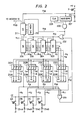
units - The detailed structure of the instruction
signal transmitting unit 20 is shown in Figure 2.Reference numerals reference numerals Reference numeral 207 indicates a monostable multivibrator (abbreviated as MNSTBMV in the figure), a numeral 208 a clock signal oscillator (abbreviated as CLK in the figure), and a numeral 209 an AND gate.Reference numeral 210 indicates a memory for starting the code of a synchronizing signal SYC (abbreviated as SYC MENM in the figure). -
Reference numerals reference numerals cameras 16A to 16D. Therefore, if there are more cameras, more code establishing circuits are employed. Also the number of push-button switches, multiple switches and shift registers will be increased accordingly. However, it should be understood that the manner of connecting these additional elements does not change in spite of an increase in the number of cameras. In particular, if the number of cameras is equal to or less than seven, it is sufficient that three further code establishing circuits which are encoded as "101", "110" and "111", respectively, are connected in parallel with the lines K5 to K7 through multiple switches provided correspondingly thereto and three shift registers are connected in cascade with the shift registers 203 to 206. Further three push-button switches must be provided to actuate the newly provided multiple switches. If the number of cameras exceeds seven, a code of three digits becomes insufficient for assigning a code to each camera. In that case, a code establishing circuit which can generate a code of more than three digits is used. - Each of
reference numerals - Each of the multiple switches 212A to 212D is equipped with three contacts which are connected to the
shift register 203 through lines K5, K6 and K7. Lines L1, L2 and L3 connect the three contacts of the multiple switch 212A to thecode establishing circuit 213A. In thiscircuit 213A, lines L1, L2 are connected to ground whereas the line L3 is connected to the positive voltage source +V. As a result, a code A is expressed in the form of a three digit signal "001". Lines L4, Ls and Ls are connected to the three contacts of themultiple switch 212B, respectively. In thecode establishing circuit 213B, the lines L4, L6 are connected to ground whereas the line L5 is connected to the positive voltage source +V. As a result, a code B is expressed in the form of a three digit signal "010". In thecode establishing circuit 213C, a line L7 is connected to ground and lines L8 and L9, connected to the positive voltage source +V, are connected to the three contacts of themultiple switch 212C, respectively. A code C, therefore, is expressed in the form of a three digit signal "011". In thecode establishing circuit 213D, a line L,o, connected to the positive voltage source +V, and lines L" and L12, connected to ground, are connected with the three contacts constituting amultiple switch 212D, respectively. A code D is expressed in the form of a three digit signal "100". The shift registers 203 and 204 are interconnected through three lines K14. Three lines K15 interconnect the shift registers 204 and 205. The lines K16 interconnect the shift registers 205 and 206. The remaining terminals of the 8-bit shift registers 203 to 206 are connected in cascade and grounded. Namely, a dummy of 5 bits, each having a logical value of zero, is added to each 3-bit signal generated by thecode establishing circuits 213A to 213D. Further, theshift register 206 is connected to theshift register 211 through a line K17. - A line K1 connects the
switch 2A to the multiple switch 212A. A line K2 connects theswitch 2B to themultiple switch 212B, a line K3 connects theswitch 2C to themultiple switch 212C, and a line K4 connects theswitch 2D to themultiple switch 212D. Theswitches 2A to 2D are connected with theOR gate 201 through lines Ka, Kg, K10 and K11, respectively. The ORgate 201 has its output terminal connected to theOR gate 202 through a line K12. The ORgate 202 has its output terminal connected to theshift register 203 to 206 through a line K13. Theswitch 3 is connected to themonostable multivibrator 207 and theshift register 211 through a line K18. Themonostable multivibrator 207 and theclock signal oscillator 208 are connected to the input terminals of the ANDgate 209. This ANDgate 209 has its output terminal connected to the input terminal of theOR gate 202. The ANDgate 209 is also connected to theshift register 211 through a line K19. TheSYC memory 210 is connected with theshift register 211. A line K20 provides connection between theshift register 211 and themodem 10. - Referring next to Figure 3, the detailed structure of the image
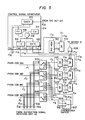
signal receiving unit 30 will be explained. - The image
signal receiving unit 30 is formed of a synchronizing signal detector (abbreviated as SYC DET in the figure), which detects the synchronizing signal SYC from the signal received by themodem 10 and produces a predetermined output will be described below. Areference numeral 302 denotes an AND gate, and areference numeral 303 indicates a re-timing circuit which extracts the clock signal from the image signal received by themodem 10. A technique for extracting a clock signal from a received signal itself is a well known technique in the field of data transmission. Areference numeral 304 denotes a control signal generator which is composed of a counter (abbreviated as CNTR in the figure) 305 and afrequency divider 306.Reference numerals 307 to 312 represent 8-bit shift registers, and areference numeral 313 denotes a changeover switch having a movingcontact 314 and two fixedcontacts - The modem 10 (Figure 1) is connected to the
shift register 309 through a line N1. A line N2 provides connection between the shift registers 309 and 308, and a line N3 interconnects the shift registers 308 and 307. Theshift register 307 is connected to theshift register 310 through lines N4. Theshift register 308 is connected to theshift register 311 through lines N5. Theshift register 309 is connected to theshift register 312 through lines N6. A line N7 connects theshift register 310 to the decoder 61 (Figure 1). Theshift register 311 is connected to thedecoder 62 through a line N8. Theshift register 312 is connected to the movingcontact 314 of thechangeover switch 313 through a line N9. The fixedcontact 315 of thechangeover switch 313 is connected to the image memory 73 (Figure 1) through a line N10 and theother contact 316 to theimage memory 74 through a line N11. - A line N12, connected to the modem 10 (Figure 1), is connected to one of the input terminals of the AND
gate 302. The synchronizingsignal detector 301 connected to the line N12 is connected with the other input terminal of the ANDgate 302. There-timing circuit 303, connected with the output terminal of the ANDgate 302, is connected to the shift registers 307, 308 and 309 through a line N,3 and to thecontrol signal generator 304 through a line N14. In thecontrol signal generator 304, the signal coupled through the line N14; which is the clock signal reproduced by there-timing circuit 303, is counted by thecounter 305, so that control signals CE and CR are generated in accordance with the contents of thecounter 305. The control signal CR is coupled to the shift registers 310 to 312 through a line N15, and the control signal CE is coupled to thechangeover switch 313 through a line N17. The control signal CE functions as a changeover signal which repeatedly changes the connection of the movingcontact 314 with the fixedcontacts control signal generator 304, thefrequency divider 306 reduces the frequency of the clock signal down to one third. Namely, thefrequency divider 306 produces one output pulse for every three pulses of the clock signal, and the output pulse is coupled to the shift registers 310 to 312 as a control signal Co through a line N16. As described above, thecontrol signal generator 304 has the function of generating various types of control signals CR, CQ, CE at respective predetermined timings on the basis of the reproduced clock signal. Therefore, it will be easily understood by one skilled in the art that such a control signal generator may be constructed by a microcomputer which is so programmed as to generate the control signals in the manner as described above. - The above explanation relates to the component parts of the monitoring site, i.e. to the instruction
signal transmitting unit 20 and the imagesignal receiving unit 30. The following explanation relates to the component parts of the remote site. - Referring at first to Figure 4, the detailed structure of the instruction
signal receiving unit 40 will be described. Thisunit 40 is equipped with a synchronizing signal detector (abbreviated as SYC DET in the figure) 401, an ANDgate 402, are-timing circuit 403 which has the same function as there-timing circuit 303 in Figure 3., a 1/8frequency divider 404, a counter (abbreviated as CNTR) 405, a shift register (abbreviated as SR) 406, comparators (abbreviated as COMPTR) 407A, 407B, 407C and 407D, shift registers (similarly abbreviated as SR) 408A, 408B, 408C and 408D, andcode establishing circuits circuits 213A to 213D of Figure 2 and produce the output signals (code) corresponding thereto, respectively. Further, the same reference numerals used in Figure 1 indicate the same component parts as shown in that figure. - The modem 12 (Figure 1) is connected to the
shift register 406 through a line E1. Lines E2, E3 and E4 connected to theshift register 406 are connected to thecomparators 407A to 407D. Lines L1, L2 and L3 connect thecode establishing circuit 409A with thecomparator 407A. Similarly, lines L4 to L6 connect thecode establishing circuit 409B with thecomparator 407B. Further, lines L, to Lg connect thecircuit 409C with thecomparator 407C and lins L10 to L12 connect thecircuit 409D with thecomparator 407D. Thesecomparators 407A to 407D have their respective output terminals connected to the shift registers 408A to 408D through lines E5 to Es, respectively. The ANDgate 402 has two input terminals, one being connected to the line E1 through a line Eg and the other to thesynchronizing signal detector 401 through a line Eio. An output terminal of the ANDgate 402 is connected to there-timing circuit 403. Theretiming circuit 403 is connected with thefrequency divider 404 and theshift register 406 through a line E11. Lines E12 to E14, connected to thecounter 405, are coupled to theshift registers 408A to 408D. Three lines E15 are connected to theshift register 408A, three lines E16 are connected to theshift register 408B, three lines E17 to theshift register 408C, and three lines E18 to theshift register 408D. These four sets of three lines E15 to E18 and the line E10 are coupled to the imagesignal transmitting unit 50. - Figure 5 shows the structure of the image
signal transmitting unit 50, which comprises shift registers (abbreviated as SR in the figure) 501 to 506 and 511, an ORgate 508, achangeover switch 507 having a moving contact and two fixedcontacts 509 and 510 as the changeover switch 313 (Figure 3), a synchronizing signal memory (abbreviated as SYC MEM) 512 which is similarto the memory 210 (Figure 2), selectingswitch circuits 513B control signal generator 514. Thecontrol signal generator 514 has atimer 515 initiated by the synchronizing signal SYC from the detector 401 (Figure 4), a flip-flop circuit (abbreviated as FF) 516, a clock signal oscillator (abbreviated as CLK) 517, an ANDgate 518, a 1/3frequency divider 519 and a counter (abbreviated as CNTR) 520. Thecontrol signal generator 514 has the function of generating various types of timing and control signals CL, CP1, CP2, Cw, CT and Cu at respective predetermined timings as discussed below, initiated by the synchronizing signal SYC. Therefore, similarly to the case of thecontrol signal generator 304 in Figure 3, this control signal generator also can be constructed of a microcomputer which is so programmed as to generate the timing and control signals in the manner as described above. Further, the same reference numerals as used in Figures 1 and 4 indicate the same component parts as shown in those figures. - The
switch circuit 513A has a movable contact connected to theencoder 18A (Figure 1) through a line F1. Theswitch circuit 513B has a movable contact connected to theencoder 18B through a line F2. Theswitch circuit 513C has a movable contact connected to theencoder 18C through a line F3. Theswitch circuit 513D has a movable contact connected to theencoder 18D through a line F4. A line F5 connected to respective fixedcontacts 1 of theswitch circuits 513A to 513D is led to theshift register 501. A line F6 connected to respective fixedcontacts 2 of theswitch circuits 513A to 513D is coupled to theshift register 502. A line F7, connected to respective fixedcontacts 3 of theswitch circuits 513A to 513D, is coupled to a fixed contact 509 of thechangeover switch 507. A line F8, connected to respective fixedcontacts 4 of theswitch circuits 513A to 513D, is coupled to the otherfixed contact 510 of thechangeover switch 507. A line Fg, connected to the movable contact of thechangeover switch 507, is coupled to theshift register 503. The shift registers 501 and 504 are interconnected through lines Flo; the shift registers 502 and 505 interconnected through lines F11, and the shift registers 503 and 506 interconnected through lines F,2. Further, the shift registers 504 to 506 are connected in series with one another through lines F,3. Theshift register 504 has an output terminal connected to one of the input terminals of theOR gate 508 through a line F14. This ORgate 508 has an output terminal connected to the modem 12 (Figure 1). - A line F15, connected to the
control signal generator 514, is coupled to thecameras 16A to 16D (Figure 1) and theshift register 511. A line F16 provides a connection between the shift registers 501 to 503 and thecontrol signal generator 514. A line F17 from thecontrol signal generator 514 is coupled to theshift register 511. Lines F18 and F19 from thecontrol signal generator 514 are both connected with theshift register 504 to 506. Thecontrol signal generator 514 and thechangeover switch 507 are connected to each other through a line F20. The lines E,5 to E18, connected to theshift registers 408A to 408D of the instruction signal receiving unit 40 (Figure 4), respectively, are connected to the selectingswitch circuits 513A to 513D. In response to the signal coupled through the corresponding one of the lines E15 to E18, each movable contact of the selectingswitch circuits 513A to 513D selects one contact among the fixedcontacts 1 to 4. - In the
control signal generator 514, thetimer 515 starts counting of time upon receipt of the signal from the synchronizing signal detector 401 (Figure 4) and produces an output signal after a period corresponding to the duration in which the logic operation in the instructionsignal receiving unit 40 is completed and thereby the signals of the lines E15 to E18 are produced. This output signal of thetimer 515 becomes the signal CT which is coupled to thecameras 16A to 16D (Figure 1) and theshift register 511 through the line F15. Thetimer 515 produces a further output at a predetermined time after production of the signal CT. Another output of thetimer 515 becomes the signal Cu coupled to thechangeover switch 507 as a changeover signal through the line F2o. When thetimer 515 produces the signal CT, the flip-flop circuit 516 is set, so that the clock signal from theclock oscillator 517 is coupled to the 1/3frequency divider 519 and thecounter 520 through the ANDgate 518. The clock signal whose frequency is reduced down to one third, is coupled to the shift registers 501 to 503 as the signal Cw through the line F16. Thecounter 520, counting the clock signal, produces the signals CL, Cp, and CP2 in accordance with its contents. The signals CL and CP2 are coupled to the shift registers 504 to 506 through the line F19 and F18, respectively, and the signal CP1 is coupled to theregister 511 through the line F17. - Next, the monitoring operations of the plant by the image transmission system having the structure thus far described according to the present embodiment will be described.
- Referring back to Figure 2, when an operator at the monitoring site depresses the push-button switches in the order of, for example, 2A, 2C, 2B and 2D, electrical current flows through the lines K1, K3, K2 and K4 one after another to render the multiple switches conductive in the order of 212A, 212C, 212B and 212D while current is flowing. The three contacts of each multiple switch are simultaneously closed. As those multiple switches are closed, codes "A", "C", "B" and "D" set in the
code establishing circuits signal transmitting unit 20 including the shift registers and the monostable multivibrator are assumed to be reset under the initial conditions. The reset signals and their input terminals are not shown. The initial values are reset as explained below. The codes thus input to theshift register 203 are then transferred sequentially to the shift registers 204 to 206 through the lines K14, K15 and K16. These code shifting operations among the shift registers 203 to 206 are conducted by applying the ON signals of theswitches 2A to 2D to the shift registers 203 to 206 through theOR gate 201, the line K,2, theOR gate 202 and the line K,3. - Figure 6 shows the states in which the shift registers 203 to 206 are being stored with the respective codes by closing the
switches switch 2A is closed whereas the remaining switches are left open, in which theshift register 203 stores the code "A". The duration denoted by T3 shows the state after theswitch 2C is closed, whereas the remaining switches are all open, in which the shift registers 204 stores the code "A", whereas theshift register 203 stores the code "C". The duration denoted by T4 indicates the state after theswitch 2B is closed, whereas the remaining switches are open, in which theshift register 205 stores the code "A", theshift register 204 stores the code "C", and theshift register 203 stores the code "B". Finally, the duration denoted by T5 indicates the state after theswitch 2D is closed, whereas the remaining switches are all open, in which the shift registers 206, 205, 204 and 203 store the codes "A", "C", "B" and "D", respectively. - It is to be noted here that the order of the codes "A", "B", "C" and "D" stored in the shift registers 206 to 203 can be arbitrarily changed by varying the order of manipulation of the
switches 2A to 2D by the operator. This manipulation order has significance in the assignment of transmission channels. Namely, in this embodiment, the frequency bandwidth of thetransmission line 14 is divided into three transmission channels, and as will be understood from the explanation below, two of the three channels are assigned to the transmission of image signals for full motion images (called a full motion image transmission, hereinafter) and the remaining one channel is assigned for image signal transmission for frame repetition images (called a frame repetition image transmission, hereinafter). This assignment of transmission channels is determined by the order of storing the codes "A" to "D" in the shift registers 206 to 203, that is to say, the order of manipulation of theswitches 2A to 2D. In this embodiment, therefore, the image signals generated by thecamera cameras - After the
switches 2A to 2D have been operated, as described above,switch 3, which has been left open, is closed by the operator. The operation of the instructionsignal transmitting unit 20 after operation of theswitch 3 could be explained, referring to Figure 7. When theswitch 3 is closed (Figure 7(a)), themonostable multivibrator 207 outputs the signal which is shown in Figure 7(b). The time during which the output signal of themultivibrator 207 is high, i.e. the so-called time constant of themultivibrator 207, is determined in dependence on the length of the instruction signal described later in reference to Figure 7(f). Theclock signal oscillator 208 outputs the clock signal which is shown in Figure 7(c). As a result, the ANDgate 209 outputs the signal which is shown in Figure 7(d). The shift register 111 receives the ON signal of theswitch 3 through the line K18 to store the synchronizing signal SYC which is read out from thememory 210. The pulse signal supplied from the ANDgate 209 is transmitted through the lines K13 and K19 to the shift registers 203 to 206 and 211. In response to the pulse signal, theseshift registers 203 to 206 and 211 conduct their shifting operations. In Figure 7(e), this operation is shown as a change of contents of the reigster only with respect to theshift register 211. As a result of the shifting operation, the synchronizing signal SYC and the codes stored in the shift registers 211, 206, 205, 204 and 203 are shifted from theshift register 211 to themodem 10 sequentially in the order as shown in Figure 7(f). The code signal "D" last stored in theshift register 203, for example, is shifted in the order of the shift registers 204, 205, 206 and 211. The signal thus shifted out of theshift register 211 to the line K20 by the shifting operations becomes the instruction signal which is headed by the synchronizing signal SYC followed by respective one-byte signals set with the codes A, C, B and D, respectively as shown in Figure 7(f). The shift registers 203 to 206 and 211, the multiple switches 212A to 212D and thecode establishing circuits 213A to 213D have functions to prepare and output the instruction signals for assigning the full motion images and the frame repetition images. As will be described later, the codes stored in the shift registers 206 and 205 correspond to the full motion imges, whereas the codes stored in the shift registers 204 and 203 correspond to the frame repetition images. More specifically, the two codes A and C following the synchronizing signal SYC of the instruction signal are assigned to the full motion images, whereas the subsequent two codes B and D are assigned to the frame repetition images. - Here, the following is to be noted with respect to the instruction
signal transmitting unit 20. In Figure 2, the structure of thisunit 20 is illustrated as a combination of various types of discrete circuits for the purpose of facilitating better understanding of the function of the instruction signal generation. Briefly speaking, as is described above, the generation of the instruction signal comprises the following steps. Namely at a first step, the code signals assigned to the cameras equipped at the sites to be monitored are produced in accordance with the order of selection of the cameras, i.e. the order of manipulation of the push-button switches 2A to 2D. In a second step, the synchronizing signal SYC is inserted at the head of the train of the code signals. Finally, the thus obtained instruction signal is sent to themodem 10. As will be understood, the instruction signal can be attained by a microcomputer which is so programmed as to execute the above steps. - The instruction signal is transmitted through the
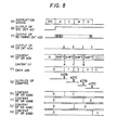
transmission line 14 to themodem 12 of the site to be monitored and further to the instructionsignal receiving unit 40. Referring to Figures 4 and 8, the operation of the instructionsignal receiving unit 40 will be described. - In the instruction
signal receiving unit 40, the received instruction signal as shown in Figure 8(a) is coupled to thesynchronizing signal detector 401 and theshift register 406. Thedetector 401 detects the synchronizing signal SYC and outputs a signal which is shown in Figure 8(b). There-timing circuit 403 having received the output of thedetector 401 through the ANDgate 402 reproduces and generates the clock signal which is shown in Figure 8(c). The 1/8frequency divider 404 divides the frequency of the reproduced clock signal to produce the signal which is shown in Figure 8(d). Thecounter 405 counts the output of the 1/8frequency divider 404 to produce the counted values as 1, 2, 3 and 4 sequentially, as shown in Figure 8(f). Theshift register 406 receives the reproduced clock signal through the line Ell, so that the instruction signal is shifted thereinto. However, it is to be noted here that, as is apparent from Figure 8(c), the clock signal is not yet reproduced when the synchronizing signal SYC reaches theshift register 406. Accordingly, the synchronizing signal SYC is not taken into theshift register 406, but theregister 406 load only the code signals A to D following the synchronizing signal SYC, bit by bit, in response to the clock signal. The change of the contents of theshift register 406 is shown in Figure 8(e). The portions indicated by "shift" in Figure 8(e) represent that the digital signal composing the respective codes are shifted sequentially in theshift register 406. To the lines E2, E3 and E4, there are separately coupled the three binary signals representative of each code. The following description will be made of the case in which the code "A" composed of "001" is coupled from theshift register 406, as has been described hereinbefore. Then, the values "0", "0" and "1" are simultaneously applied to the lines E2 to E4, respectively. Therespective comparators 407A to 407D generates output signals only when the signal coupled from theshift register 406 and the output signals of thecode establishing circuits 409A to 409D are coincident with each other. Since, in the example of this embodiment, the code signals are arranged in the order of "A", "C", "B" and "D", thecomparators 407A to 407D sequentially generate the signals as shown in Figure 8(g). - The output of the
counter 405 is coupled to all theshift registers 408A to 408D. The outputs of thecomparators 407A to 407D are also coupled to thecorresponding shift registers 408A to 408D as an input timing signal. In response to the timing signal, theshift registers 408A to 408D are loaded with the contents of thecounter 405 at that time. Consequently theshift registers 408A to 408D store the counted values, as shown in Figures 8(h) to 8(k). In this embodiment, the counted values are 1, 3, 2 and 4, respectively. As described above, thecounter 405, thecomparators 407A to 407D and theshift registers 408A to 408D select the cameras for full motion images and the cameras for frame repetition images in response to the instruction signal mentioned above. For thecamera 16A, thecounter 405, thecomparator 407A and theshift register 408A determine whether full motion or frame repetition image signals are to be generated. For thecamera 16B, thecounter 405, thecomparator 407B and theshift register 408B determine whether full motion of frame repetition image signals are to be generated. Thecounter 405, thecomparator 407C and theshift register 408C determine whether thecamera 16C is to generate full motion or frame repetition image signals. Thecounter 405, thecomparator 407D and theshift register 408D determine whether thecamera 16D is to generate signals, for the full motion or frame repetition images. - Briefly speaking, as described above, the
instruction receiving unit 40 discriminates the order of the code signals A to D included in the received instruction signal. To this end, thisunit 40 has the function of decoding the instruction signal which comprises the following steps: generating the codes corresponding to the codes assigned to the cameras; comparing each of the thus generated codes with the successively received code signals one after another; and discriminating the order of reception of the code signals on the basis of the above comparison to produce a contact selecting signal to the selecting switch circuits. All of these steps can be achieved by a usual microcomputer, so that, similarly to the instructionsignal transmitting unit 20 shown in Figure 2, the instructionsignal receiving unit 40 also can be constructed by a microcomputer which is so programmed as to execute the above mentioned steps. - Now, the contents stored in the
shift register 408A to 408D are coupled to the imagesignal transmitting unit 50 through the lines E15 to E18. In thisunit 50, the image signals which are picked up by thecameras 16A to 16D and converted into digital signals by theencoders 18A to 18D are processed to be formed into an image signal suitable for transmission to the imagesignal receiving unit 30 at the monitoring site in accordance with the instruction signal decoded in the instructionsignal receiving unit 40, as mentioned above. The operation of the imagesignal transmitting unit 40 will be explained in the following, referring to Figures 5 and 9. - In Figure 5, the signals which are coupled through the lines E15 to E18 are given to the selecting
switch circuits 513A to 513D as the contact selecting signals, respectively. Each of these signals determines one of four fixed contacts to be selected by the movable contacts. Although, as is apparent from the foregoing description, each of these signals represents one of thenumerical values 1 to 4, the numerical value corresponds to the number of the fixed contact to be selected, as shown in the figure. Accordingly, the signal transmitted through the line E15 is coupled to theswitch circuit 513A. Thisswitch circuit 513A connects the movable contact to the fixedcontact number 1, since the numerical value of this signal is 1. Since theswitch circuit 513B receives the signal through the line E16, which represents thenumerical value 3, the movable contact thereof selects the fixedcontact number 3. Similarly, since theswitch circuit 513C receives the signal through the line E17, which represents thenumerical value 2, the movable contact thereof is connected to the fixedcontact number 2. Further, since theswitch circuit 513D receives the signal through the line E18, which represent thenumerical value 4, the movable contact selects the fixedcontact number 4. The selectingswitch circuits 513A to 513D are switching means to connect the respective cameras with a full motion or a frame repetition image transmission means in accordance with the aforementioned camera selecting function of the instructionsignal receiving unit 40. - The image signal output from the
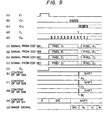
cameras 16A to 16D is synchronized with the signal CT, as shown in Figure 9(a), which is transmitted from thecontrol signal generator 514 through the line F15. As has been already described, the signal CT is coupled from thecontrol signal generator 514 after the signals on the lines E15 to Els have been produced. Moreover, the signal CT is coupled through the line F,5 to theshift register 511. Thisshift register 511 receives and stores the synchronizing signal SYC from thememory 512. The image signals generated by thecameras 16A to 16D are coupled to theencoders 18A to 18D so that they become pixel signals which are shown in Figures 9(f) to 9(i). The pixel signal coupled from theencoder 18A is applied to theshift register 501 through the lines F, and F5. The pixel signal coupled from theencoder 18C is coupled to theshift register 502 through the lines F3 and F6. The pixel signal coupled from theencoder 18B is transmitted to thechangeover switch 507 through the lines F2 and F7. The pixel signal coupled from theencoder 18D is transmitted to thechangeover switch 507 through the lines F4 and Fo. As described before, thechangeover switch 507 has its movable contact connected alternately at a predetermined interval with the fixed contact 509 connected to the line F7 and the fixedcontact 510 connected to the line Fa. This switching operation of the movable contact is conducted each time the image signals from theencoders changeover switch 507 is concudcted in response to the signal Cu which is coupled from thecontrol signal generator 514 to thechangeover switch 507 through the line F2o. Here assumed that the movable contact of thechangeover switch 507 will be connected with the fixed contact 509. Then, the pixel signal from theencoder 18B is coupled to theshift register 503. The storage of the pixel signals in theshift register 501 to 503 is conducted in synchronism with the signal Cw, as shown in Figure 9(E), which is coupled from thecontrol signal generator 514 after the signal CT has the value "0". When a signal CL shown in Figure 9(d) is applied to theshift register 504 to 506, pixel signals A1, C1 and B, stored in the shift registers 501 to 503 are transferred to and stored in thecorresponding shift register 504 to 506 (as shown in Figures 9(k) to 9(m). Theshift register switching circuit 507 and theshift register - Before the signal CL is coupled from the
control signal generator 514, a signal CP1 is coupled from the same, as shown in Figure 9(b). Theshift register 511 receives the signal CP1 through the line F17 to couple the stored synchronizing signal SYC to themodem 12 through theOR gate 508. The signal CP1 is interrupted simultaneously with the interruption of the signal CL. As soon as the signal CP1 is interrupted, a signal CP2 is coupled from thecontrol signal generator 514. When the signal CP2 is applied to theshift register 504 to 506, the pixel signals A1, C1 and B1 stored in those shift registers are transmitted in series to themodem 12 through theOR gate 508. As a result, an image signal headed by the synchronizing signal SYC, as shown in Figure 9(p), is coupled from themodem 12 to thetransmission line 14. - The details of the image signal transmitted from the
modem 12 is shown in Figure 10. This figure shows the formation of the image signal of k-th and (k+1)th frames with respect to the image signals A and C generated by thecameras cameras shift register 504, they are accompanied by successive pixel signals A2, C2 and B2 until pixel signals An, Cn and Bn are finally produced. The pixel signals Alto An form one frame of the image A, the pixel signals C1 to Cn form one frame of the image C, and the pixel signals B1 to Bn form one frame of the image B. When the pixel signal Bn is coupled, the movable contact ofchangeover switch 507 is connected with the fixedcontact 510 thereof, so that the pixel signal D1 is stored in theshift register 503 and further in theshift register 506. As a result, the pixel signals A1, C1, D1, A2, C2, D2 and so on are sequentially produced in the same manner as described above. - A variation of assignment of channels to the full motion image and the frame repetition image transmissions can be achieved by changing the wiring between the selecting
switch circuits 513A to 513D and the shift registers 501, 502 and thechangeover switch 507. If a changeover switch having three fixed contacts is substituted for the two-fixed-contact changeover switch 507, as used in Figure 5, and the line F6 is connected to a third fixed contact. thereof, it can be realized that only one channel is assigned for full motion image transmission, and the remaining two channels may be employed for frame repetition image transmission. - Further, another variation can be considered. Where the
transmission line 14 is divided into more than three channels, there must be provided a number of selecting switch circuits corresponding to the number of channels. The number of fixed contacts of each of such selecting switch circuits also must correspond to the number of channels. On the other hand, the number of fixed contacts of the changeover switch is determined in dependence on how many channels are assigned to the full motion image transmission. For example, where the transmission line is divided into 50 channels and two channels thereamong are assigned to full motion image transmission, 48 fixed contacts are necessary in the changeover switch. The wiring between the selecting switch circuits and the changeover switch can be easily done in accordance with that way shown in Figure 5. In this case, the arrangement of theshift register 501 to 506 does not change, since two channels are assigned to full motion image transmission in the same manner as in Figure 5 and a single shift register for storing the image signal of the frame repetition image is used by changing the image signals for every frame repetition image transmission. These modifications and variation mentioned above can be easily performed by one skilled in the art. - The above mentioned image signal obtained in the image
signal transmitting unit 50 is transmitted from themodem 12 through thetransmission line 14 to the monitor room and received by themodem 10. Next, the operation of the imagesignal receiving unit 30 which is supplied with the image signal received by themodem 10, will be described referring to Figures 3 and 11. - The image signal received by the
modem 10 is coupled to theshift register 309 through the line N1 and the synchronizingsignal detector 301 through the line N12. This synchronizingsignal detector 301 receives the image signal as shown in Figure 11 (a) to generate a signal as shown in Figure 11(b). This output is coupled through the ANDgate 302 to there-timing circuit 303. Thiscircuit 303 outputs a clock pulse signal which is shown in Figure 11 (c). This pulse signal is coupled to thecontrol signal generator 304 as well as to the shift registers 307 to 309. As a result, theseshift registers 307 to 309 store the pixel signals A1, C1 and B1. More specifically, theshift register 307 stores the pixel signals (A1, A2, ..., and An) pixel by pixel, as shown in Figure 11 (e). Theshift register 308 stores the pixel signals (C1, C2, ..., and Cn) pixel by pixel, as shown in Figure 11(f). Theshift register 309 stores the pixel signals (B1, B2, ..., and Bn) pixel by pixel, as shown in Figure 11 (g). Here, it is to be noted that the synchronizing signal SYC included in the received image signal is not set into the shift registers 307 to 309, since the clock signal is not yet reproduced when the synchronizing signal SYC is coupled toshift register 309. - A signal CR (as shown in Figure 11(d)) is coupled from the
control signal generator 304 to the shift registers 310 to 312. In response to the signal CR, the shift registers 310 to 312 store the pixel signals A1, C1 and B1 stored in thecorresponding shift registers 307 to 309, as shown in Figures 11 (h) to (j). Next, a signal Co (as shown in Figure 11 (k)) generated by thecontrol signal generator 304 is coupled to the shift registers 310 to 312. At this time, the shift registers 310 to 312 output the pixel signals stored therein. The pixel signals (A1, A2, ..., and An) sequentially drifted out from theshift register 310 are represented as the image signals to thedecoder 61. Thedecoder 61 decodes and decompresses the digital, bandwidth-compressed image signal, so that thetelevision monitor 81 displays the image which has been detected thecamera 16A. The pixel signals (C1, C2, ..., and Cn) outputted from theshift register 311 are transmitted as the image signals to thedecoder 62. Thedecoder 62 decodes and decompresses the digital, bandwidth-compressed image signals, so that thetelevision monitor 82 displays the image which has been detected by thecamera 16C. Thechangeover switch 313 receives the signal CE (as shown in Figure 11 (p)) provided by thecontrol signal generator 304 and has itsmovable contact 314 connected with the fixedcontact 315. As a result, the pixel signals (Bi, Ba,..., and Bn) coupled from theshift register 312 are stored in thememory 73. The pixel signals stored in thememory 73 are coupled to thedecoder 63, and are decoded and decompressed, so that thetelevision monitor 83 displays the image which has been detected by thecamera 16B. Themovable contact 314 is so controlled by the signal CE that it is connected with the fixedcontact 315, when the movable contact of the changeover switch 507 (Figure 5) is connected with the fixed contact 509, and with the fixedcontact 316 when the movable contact of thechangeover switch 507 is connected with the fixedcontact 510. When the state of the signal C, changes (the change of state is not shown in Figure 11 (p)), themovable contact 314 of thechangeover switch 313 is connected to the fixedcontact 316. At that time, the pixel signals (D,, D2, ..., and Dn) are stored in theshift register 312, so that they are stored in thememory 74 through thechangeover switch 313. The pixel signals stored in thememory 74 are coupled to thedecoder 64, decoded and decompressed. Consequently, thetelevision monitor 84 displays the image which has been detected by thecamera 16D. It should be noted that the pixel signals are stored in both thememories - As described above, the image signals displayed by the
television monitor memories television monitor memories - Next, an example of the effects of the present embodiment will be explained with reference to Figure 12.
- First of all, the following conditions are assumed. The transmission line has the capability of a transmission rate of 96 Mbps, and by using the appropriate bandwidth compression method, e.g. a two- dimensional predictive coding scheme, the image signal is compressed to a digital signal of 4 bits per pixel. In order that such a digital signal may be transmitted at the 4MHz base frequency, the frequency bandwidth required of the transmission line corresponds to 32 Mbps (4 MHzx2x4 bits). Therefore, a transmission line with a capability of 96 Mbps as mentioned above can be divided into 3 transmission channels, each having an equal rate of 32 Mbps. Further, let us assume here that one frame of a picture is composed of 512x512 pixels, which corresponds to about 1049 K bits in the digital image signal. Where a frame of picture is transmitted through the transmission channel having a transmission rate of 32 Mbps, the time necessary for completing the transmission of one frame becomes about 33 ms (1049 K bits-32 Mbps). Accordingly image signals for about 30 frames can be transmitted every second through one transmission channel. If two channels, i.e. having a capability of 64 Mbps, are used, image signals for 60 frames can be transmitted every second, and further, those for 90 frames can be transmitted in the case of three channels, i.e. by using the full capability (96 Mbps) of the transmission line. Actually, however, 32 Mbps, i.e. 30 frames per second, is a rate sufficient to reproduce a full motion image at the monitoring side. Namely, the reproduction of a full motion image of a remote site to be monitored becomes possible, if the image signals of the remote site can be transmitted at a rate of 30 frames/sec. Therefore, more than one channel need not necessarily be assigned to full motion image transmissions for one site being monitored.
- In the present embodiment two channels of the line, which is divided into three transmission channels, are assigned to full motion image transmission for two sites which are monitored by the
cameras cameras - Figure 12 is a graph showing the relationship between the transmission rate of a frame repetition image (frames/s/site) and the number of channels assigned to full motion image transmission (NM) as mentioned above, for respective numbers of frames by frame repetition image transmission. As is apparent from the figure, if only one channel is assigned to the full motion image transmission and the transmission rate for the frame repetition image is, for example, about 0.7 frames/s/site, 90 sites can be monitored by the frame repetition image through the remaining two channels.
- Here, an example of the actual application of this embodiment, in which there are provided 92 sites to be monitored in a plant or building will be described. Usually, i.e. when there is no malfunction or abnormal state in the plant or building, two channels of the transmission line are assigned to the full motion image transmission for two sites arbitrarily selected among the 92 sites to be monitored, and the remaining one channel is assigned to frame repetition image transmission for the remaining 90 sites to be monitored. At this time, as is understood from Figure 12, the transmission rate of frame repetition image transmission is about 0.3 frames/sec/site (cf. a point on the Ns=90 line with respect to NM=2). If a malfunction or abnormal state among the above mentioned 90 sites has been observed from the display of the frame repetition image, the operator can change the display of the image of the respective site from frame repetition image to full motion image by manipulating the push-
button switches 2A to 2D (Figure 1 Namely, if an abnormal condition at the remote site has been observed by thecamera 16D from the display of thetelevision monitor 84, which is in frame repetition image state, the operator re-manipulates the push-button switches so that theswitch 2D is at first depressed, preceding the manipulation of the other push-button switches. Consequently, the image signal picked up by thecamera 16D is transmitted by full motion image transmission. Thus, according to the present embodiment, a system is provided in which the channel or channels can be preferentially assigned to the monitoring operations of the sites having high importance or emergency by means of the full motion images, whereas the remaining channels can be assigned to the monitoring operations of the remaining sites by means of the frame repetition images, so that the limited capacity of the transmission line can be effectively utilized and the system can be suitably applied for monitoring hundreds of sites such as a large plant or building. With the television monitor which display full motion images, the image transmission period is so short that the monitoring operations can be conducted almost in a real time base. With television monitors which display frame repetition images, the transmission period for each image is long, but the images of a base number of TV cameras can be monitored. - In the present embodiment, the portions of the image
signal transmitting unit 50 storing image signals of frame repetition images have simplified structures because of the limited number of shift registers. In the imagesignal receiving unit 30, the portions (e.g., the shift registers 309 and 312) storing the image signals of frame repetition images have simplified structures. Since the image signals of plural cameras for frame repetition images are stored alternately in one image storage, the structures of the storages device for storing frame repetition images can be simplified so that the structures of the respective units can be simplified. - Another embodiment of the present invention is shown in Figure 13. The same reference characters as those of the embodiments of Figure 1 indicate the same parts. In this embodiment,
reference numerals reference numerals change detection circuit reference numeral 951 indicates an image memory for storing a frame, e.g., 512 x 512 picture elements.Reference numeral 952 designates an image memory for storing the last frame, and areference numeral 953 designates an image comparator for computing the sum of the difference between the pixel values of thememories reference numeral 954 indicates a threshold circuit which generates an output when the sum of the difference of the pixel values of thecomparator 953 exceeds a predetermined value, causing thealarm lamp - Usually, the operator watches the
monitor television sets alarm lamp circuit cameras 16A to 16D corresponding to thealarm lamp television monitor switches 2A to 2D and 3. Further, by cooperating the operation of theswitches 2A to 2D and 3 with the outputs of the imagechange detection circuits cameras 16A to 16D corresponding to thealarm lamp
Claims (5)
Applications Claiming Priority (2)
| Application Number | Priority Date | Filing Date | Title |
|---|---|---|---|
| JP5743/85 | 1985-01-18 | ||
| JP60005743A JPS61166289A (en) | 1985-01-18 | 1985-01-18 | Picture transmission system |
Publications (3)
| Publication Number | Publication Date |
|---|---|
| EP0188286A2 EP0188286A2 (en) | 1986-07-23 |
| EP0188286A3 EP0188286A3 (en) | 1986-11-26 |
| EP0188286B1 true EP0188286B1 (en) | 1990-11-28 |
Family
ID=11619582
Family Applications (1)
| Application Number | Title | Priority Date | Filing Date |
|---|---|---|---|
| EP86100485A Expired - Lifetime EP0188286B1 (en) | 1985-01-18 | 1986-01-16 | Image transmission system |
Country Status (5)
| Country | Link |
|---|---|
| US (1) | US4673974A (en) |
| EP (1) | EP0188286B1 (en) |
| JP (1) | JPS61166289A (en) |
| KR (1) | KR920005019B1 (en) |
| DE (1) | DE3675780D1 (en) |
Cited By (3)
| Publication number | Priority date | Publication date | Assignee | Title |
|---|---|---|---|---|
| US7835509B2 (en) | 1993-03-12 | 2010-11-16 | Telebuyer, Llc | Commercial product routing system with video vending capability |
| US8059796B2 (en) | 1993-03-12 | 2011-11-15 | Telebuyer, Llc | Commercial product routing system with video vending capability |
| US8315364B2 (en) | 1993-03-12 | 2012-11-20 | Telebuyer, Llc | Commercial product telephonic routing system with mobile wireless and video vending capability |
Families Citing this family (45)
| Publication number | Priority date | Publication date | Assignee | Title |
|---|---|---|---|---|
| JP2528789B2 (en) * | 1985-06-26 | 1996-08-28 | 中央電子 株式会社 | Video information management device |
| JPS62265878A (en) * | 1986-05-13 | 1987-11-18 | Sony Corp | Monitor device |
| JPH07101936B2 (en) * | 1986-05-30 | 1995-11-01 | ソニー株式会社 | Monitoring device adapter |
| JPS633590A (en) * | 1986-06-23 | 1988-01-08 | Sony Corp | Monitor device |
| WO1988004082A1 (en) * | 1986-11-25 | 1988-06-02 | Zone Technology Pty. Limited | Digital image acquisition system |
| US4831438A (en) * | 1987-02-25 | 1989-05-16 | Household Data Services | Electronic surveillance system |
| US4814869A (en) * | 1987-04-27 | 1989-03-21 | Oliver Jr Robert C | Video surveillance system |
| US4779134A (en) * | 1987-05-28 | 1988-10-18 | Mak Stephen M | Apparatus and method for viewing of multiple television stations and switching among them |
| JPS647791A (en) * | 1987-06-30 | 1989-01-11 | Nec Corp | Multiscreen video conference method and device therefor |
| JPH01181389A (en) * | 1988-01-14 | 1989-07-19 | Hitachi Ltd | Picture processor |
| JPH01218181A (en) * | 1988-02-25 | 1989-08-31 | Erubetsukusu Video Kk | Closed circuit television equipment |
| JPH01220993A (en) * | 1988-02-29 | 1989-09-04 | Erubetsukusu Video Kk | Closed circuit television equipment |
| KR930000956B1 (en) * | 1989-12-31 | 1993-02-11 | 삼성전자 주식회사 | Control apparatus for recording and reproducing a plurality of video signals |
| JPH04220823A (en) * | 1990-12-20 | 1992-08-11 | Fujitsu Ltd | Picture signal transmission control system |
| GB9101548D0 (en) * | 1991-01-24 | 1991-03-06 | Stc Plc | Surveillance system |
| US5382943A (en) * | 1991-07-31 | 1995-01-17 | Tanaka; Mutuo | Remote monitoring unit |
| WO1994010804A1 (en) * | 1992-10-27 | 1994-05-11 | Oakleigh Systems, Inc. | Access control security system using digital communication |
| US6469746B1 (en) * | 1992-12-28 | 2002-10-22 | Sanyo Electric Co., Ltd. | Multi-vision screen adapter |
| US5412708A (en) * | 1993-03-12 | 1995-05-02 | Katz; Ronald A. | Videophone system for scrutiny monitoring with computer control |
| US7019770B1 (en) | 1993-03-12 | 2006-03-28 | Telebuyer, Llc | Videophone system for scrutiny monitoring with computer control |
| JP2500582B2 (en) * | 1993-03-17 | 1996-05-29 | 日本電気株式会社 | Method and apparatus for multiplexing transmission of moving image signal |
| USRE43462E1 (en) | 1993-04-21 | 2012-06-12 | Kinya (Ken) Washino | Video monitoring and conferencing system |
| JPH07146671A (en) * | 1993-06-16 | 1995-06-06 | Mitsubishi Electric Corp | Large-sized video display device |
| CH690055A5 (en) * | 1994-04-25 | 2000-03-31 | Laurent Zwahlen | Installation and method for transmitting high-frequency taking television camera. |
| GB2305061B (en) * | 1994-07-26 | 1998-12-09 | Maxpro Systems Pty Ltd | Text insertion system |
| US6628887B1 (en) | 1998-04-17 | 2003-09-30 | Honeywell International, Inc. | Video security system |
| US5614955A (en) * | 1994-11-09 | 1997-03-25 | Michael I. Rackman | Compressed digital multi-channel video communications system having one or more auxiliary channels to accomodate high bit rates |
| JP3210209B2 (en) * | 1995-06-13 | 2001-09-17 | 松下電器産業株式会社 | Monitoring system |
| JP3112411B2 (en) * | 1996-01-11 | 2000-11-27 | 松下電器産業株式会社 | Video transmission equipment |
| US5805813A (en) * | 1996-07-26 | 1998-09-08 | Schweitzer Engineering Laboratories, Inc. | System for visual monitoring of operational indicators in an electric power system |
| GB2329539B (en) * | 1997-09-17 | 2002-05-15 | Sony Uk Ltd | Security System |
| SE522856C2 (en) * | 1999-01-29 | 2004-03-09 | Axis Ab | A data storage and reduction method for digital images, as well as a monitoring system using said method |
| US6330025B1 (en) | 1999-05-10 | 2001-12-11 | Nice Systems Ltd. | Digital video logging system |
| WO2002054221A2 (en) * | 2001-01-03 | 2002-07-11 | Nice Systems Limited | Content-based storage management |
| US6985603B2 (en) * | 2001-08-13 | 2006-01-10 | Koninklijke Philips Electronics N.V. | Method and apparatus for extending video content analysis to multiple channels |
| JP4191398B2 (en) * | 2001-08-31 | 2008-12-03 | パナソニック株式会社 | Surveillance image recording device |
| US20050007452A1 (en) * | 2001-09-07 | 2005-01-13 | Mckay Therman Ward | Video analyzer |
| NZ531976A (en) * | 2001-09-07 | 2007-07-27 | Intergraph Software Tech Co | Method, device and computer program product for demultiplexing of video images |
| US7474852B1 (en) * | 2004-02-12 | 2009-01-06 | Multidyne Electronics Inc. | System for communication of video, audio, data, control or other signals over fiber |
| US20060215024A1 (en) * | 2005-03-23 | 2006-09-28 | Coonce Charles K | Method and real time emergency response surveillances system with an emergency switch |
| US20060215023A1 (en) * | 2005-03-23 | 2006-09-28 | Coonce Charles K | Method and system of displaying user interest data at a surveillance station |
| US7336169B2 (en) * | 2005-03-23 | 2008-02-26 | Lake Star Consulting Llc | Method and real time emergency response surveillance system |
| US8498497B2 (en) * | 2006-11-17 | 2013-07-30 | Microsoft Corporation | Swarm imaging |
| KR101753572B1 (en) * | 2008-10-14 | 2017-07-04 | 코닌클리케 필립스 엔.브이. | Content item identifier |
| US20130278775A1 (en) * | 2011-10-24 | 2013-10-24 | Naveen Doddapuneni | Multiple Stream Processing for Video Analytics and Encoding |
Family Cites Families (6)
| Publication number | Priority date | Publication date | Assignee | Title |
|---|---|---|---|---|
| DE1066232B (en) * | ||||
| DE2243185A1 (en) * | 1972-09-01 | 1974-03-14 | Bosch Elektronik Gmbh | DEVICE FOR REMOTE MONITORING OF SEVERAL ROOMS |
| US4091422A (en) * | 1976-12-08 | 1978-05-23 | Gerald Amster | Apparatus for selectively transmitting television images from a plurality of cameras to a monitor |
| JPS6360960B2 (en) * | 1980-10-22 | 1988-11-25 | ||
| FR2515400A1 (en) * | 1981-10-26 | 1983-04-29 | Visiodis Sa | FDM system for remote control of surveillance cameras - uses frequency converters at remotely controlled concentrator for transposed base band signals |
| US4511886A (en) * | 1983-06-01 | 1985-04-16 | Micron International, Ltd. | Electronic security and surveillance system |
-
1985
- 1985-01-18 JP JP60005743A patent/JPS61166289A/en active Granted
-
1986
- 1986-01-07 US US06/816,841 patent/US4673974A/en not_active Expired - Fee Related
- 1986-01-16 DE DE8686100485T patent/DE3675780D1/en not_active Expired - Lifetime
- 1986-01-16 EP EP86100485A patent/EP0188286B1/en not_active Expired - Lifetime
- 1986-01-18 KR KR1019860000286A patent/KR920005019B1/en not_active IP Right Cessation
Cited By (10)
| Publication number | Priority date | Publication date | Assignee | Title |
|---|---|---|---|---|
| US7835509B2 (en) | 1993-03-12 | 2010-11-16 | Telebuyer, Llc | Commercial product routing system with video vending capability |
| US7839984B2 (en) | 1993-03-12 | 2010-11-23 | Telebuyer, Llc | Commercial product routing system with video vending capability |
| US7848496B2 (en) | 1993-03-12 | 2010-12-07 | Telebuyer, Llc | Method for buyer-seller-on-line commerce |
| US8059796B2 (en) | 1993-03-12 | 2011-11-15 | Telebuyer, Llc | Commercial product routing system with video vending capability |
| US8098272B2 (en) | 1993-03-12 | 2012-01-17 | Telebuyer, Llc | Commercial product routing system with video vending capability |
| US8111279B2 (en) | 1993-03-12 | 2012-02-07 | Telebuyer Llc | Commercial product routing system with video vending capability |
| US8315364B2 (en) | 1993-03-12 | 2012-11-20 | Telebuyer, Llc | Commercial product telephonic routing system with mobile wireless and video vending capability |
| US8836749B2 (en) | 1993-03-12 | 2014-09-16 | Telebuyer, Llc | Security monitoring system with combined video and graphics display |
| US8842151B2 (en) | 1993-03-12 | 2014-09-23 | Telebuyer, Llc | Security monitoring system with flexible monitoring sequence |
| US9053485B2 (en) | 1993-03-12 | 2015-06-09 | Telebuyer, Llc | Security monitoring system with image comparison of monitored location |
Also Published As
| Publication number | Publication date |
|---|---|
| KR920005019B1 (en) | 1992-06-22 |
| JPS61166289A (en) | 1986-07-26 |
| JPH0416996B2 (en) | 1992-03-25 |
| EP0188286A2 (en) | 1986-07-23 |
| US4673974A (en) | 1987-06-16 |
| DE3675780D1 (en) | 1991-01-10 |
| KR860006181A (en) | 1986-08-28 |
| EP0188286A3 (en) | 1986-11-26 |
Similar Documents
| Publication | Publication Date | Title |
|---|---|---|
| EP0188286B1 (en) | Image transmission system | |
| US4215369A (en) | Digital transmission system for television video signals | |
| EP0320882B1 (en) | Demultiplexer system | |
| US6049353A (en) | Computer network, processing of digitized, compressed, security camera video, intelligently onto hard drives of personal computers | |
| EP0661883A2 (en) | Method for bidirectionally transmitting digital video signal and digital video signal bidirectionally transmitting system | |
| JPS5810038B2 (en) | Communication exchange method | |
| US3849773A (en) | Apparatus for displaying characters and/or limited graphs | |
| EP0196094B1 (en) | Multi-element information transmission system | |
| JPH03243042A (en) | Method of transmitting command through serial-link | |
| US20090303328A1 (en) | Surveillance system and control apparatus therefor | |
| CN1042486C (en) | Circuit and method for generating caption signal in video signal processing system | |
| US4006297A (en) | Television signal coding system | |
| JPH02109198A (en) | Multiple point monitoring device | |
| CA1187169A (en) | Video/audio simultaneous transmission system | |
| US4951143A (en) | Memory configuration for unsynchronized input and output data streams | |
| EP0502708B1 (en) | Muse signal digital recording/reproducing apparatus and operating method thereof | |
| EP0423979B1 (en) | High definition video signal recording systems | |
| US4129751A (en) | PCM data throttle | |
| SU752412A1 (en) | Device for monitoring and controlling equipment operation | |
| SU1117861A1 (en) | Device for transmitting and receiving several broadcast programs via single conventional televison channel | |
| KR100197861B1 (en) | Apparatus for changing group number in a video conference system | |
| KR0158727B1 (en) | Sequence/non-sequence transforming apparatus of a supervisory system | |
| SU1690217A1 (en) | Tv tracking device | |
| SU1107319A1 (en) | Device for compressing television signals | |
| JPH1066062A (en) | Multi-screen display system |
Legal Events
| Date | Code | Title | Description |
|---|---|---|---|
| PUAI | Public reference made under article 153(3) epc to a published international application that has entered the european phase |
Free format text: ORIGINAL CODE: 0009012 |
|
| AK | Designated contracting states |
Kind code of ref document: A2 Designated state(s): DE GB |
|
| PUAL | Search report despatched |
Free format text: ORIGINAL CODE: 0009013 |
|
| AK | Designated contracting states |
Kind code of ref document: A3 Designated state(s): DE GB |
|
| 17P | Request for examination filed |
Effective date: 19861128 |
|
| 17Q | First examination report despatched |
Effective date: 19890317 |
|
| GRAA | (expected) grant |
Free format text: ORIGINAL CODE: 0009210 |
|
| AK | Designated contracting states |
Kind code of ref document: B1 Designated state(s): DE GB |
|
| REF | Corresponds to: |
Ref document number: 3675780 Country of ref document: DE Date of ref document: 19910110 |
|
| PLBE | No opposition filed within time limit |
Free format text: ORIGINAL CODE: 0009261 |
|
| STAA | Information on the status of an ep patent application or granted ep patent |
Free format text: STATUS: NO OPPOSITION FILED WITHIN TIME LIMIT |
|
| 26N | No opposition filed | ||
| PGFP | Annual fee paid to national office [announced via postgrant information from national office to epo] |
Ref country code: GB Payment date: 19951227 Year of fee payment: 11 |
|
| PGFP | Annual fee paid to national office [announced via postgrant information from national office to epo] |
Ref country code: DE Payment date: 19960329 Year of fee payment: 11 |
|
| PG25 | Lapsed in a contracting state [announced via postgrant information from national office to epo] |
Ref country code: GB Effective date: 19970116 |
|
| GBPC | Gb: european patent ceased through non-payment of renewal fee |
Effective date: 19970116 |
|
| PG25 | Lapsed in a contracting state [announced via postgrant information from national office to epo] |
Ref country code: DE Effective date: 19971001 |