EP0186590B1 - Control device for a phase regulator - Google Patents
Control device for a phase regulator Download PDFInfo
- Publication number
- EP0186590B1 EP0186590B1 EP19850402571 EP85402571A EP0186590B1 EP 0186590 B1 EP0186590 B1 EP 0186590B1 EP 19850402571 EP19850402571 EP 19850402571 EP 85402571 A EP85402571 A EP 85402571A EP 0186590 B1 EP0186590 B1 EP 0186590B1
- Authority
- EP
- European Patent Office
- Prior art keywords
- network
- linear
- driver device
- voltage
- correction
- Prior art date
- Legal status (The legal status is an assumption and is not a legal conclusion. Google has not performed a legal analysis and makes no representation as to the accuracy of the status listed.)
- Expired - Lifetime
Links
Images

Classifications
-
- H—ELECTRICITY
- H02—GENERATION; CONVERSION OR DISTRIBUTION OF ELECTRIC POWER
- H02M—APPARATUS FOR CONVERSION BETWEEN AC AND AC, BETWEEN AC AND DC, OR BETWEEN DC AND DC, AND FOR USE WITH MAINS OR SIMILAR POWER SUPPLY SYSTEMS; CONVERSION OF DC OR AC INPUT POWER INTO SURGE OUTPUT POWER; CONTROL OR REGULATION THEREOF
- H02M1/00—Details of apparatus for conversion
- H02M1/08—Circuits specially adapted for the generation of control voltages for semiconductor devices incorporated in static converters
- H02M1/081—Circuits specially adapted for the generation of control voltages for semiconductor devices incorporated in static converters wherein the phase of the control voltage is adjustable with reference to the AC source
Definitions
- the present invention relates to an electronic dimmer control device making it possible to adjust, as a function of a control signal, the power applied to a receiving apparatus by a substantially sinusoidal alternative electrical power source, comprising an electronic controlled switch whose the conductive state is triggered, during each half-wave of the power source, at an instant offering, relative to the end of the previous half-wave, a variable phase shift according to a correction law aimed ensuring the proportionality of the effective power applied to the receiving apparatus and of the value of the control signal on which said phase shift is dependent.
- the operating principle of electronic dimmers or dimmers of this kind is well known; it is based on variable phase control of semiconductors such as triacs or thyristors with respect to the zero crossing of the supply sinusoid.
- This command is generally carried out by means of an electronic circuit commonly called a trigger, which itself receives information in the form of a variable DC voltage, for example between 0 and 10 V, which makes it possible to have a command between 0 and 100% of the effective output voltage.
- Such dynamic correction devices known for example from documents DE-A-2 032 949 and US-A-3 942 041, give an excellent result provided that a supply voltage is perfectly sinusoidal and stable in amplitude. Against by, if one of these conditions t i ons is not fulfilled, which is the most common case for electrical distribution networks, the control of the variable current source (usually made from the supply voltage) no longer corresponds to the desired correction.
- the invention relates to a control device or trigger of the kind defined at the start, in which the phase shift of the instant of tripping of the controlled switch is created in proportion to the value d a continuous signal which varies with the control signal in accordance with said law of correction by means of a function generator.
- This arrangement is advantageous in that the correction is carried out independently of the voltage of the AC power source (in its form and especially in its amplitude), and this in a static manner, that is to say that 'to a fixed control quantity corresponds a corrected continuous signal also fixed, which allows better control of phenomena and increased precision.
- Said continuous signal is preferably generated, from the control signal, by a function generator providing, thanks to a non-linear network, an approximation by connected rectilinear segments of the correction law.
- the non-linear network is designed to provide the approximation by rectilinear segments only of one of the halves of said curve, while an auxiliary switching network associated with this network allows it to provide the approximation of one and the other of the symmetrical halves. A perfect symmetry of correction is thus obtained on either side of said central point.
- the non-linear network can then comprise a linear section and a non-linear section, while only the non-linear section is switched by the auxiliary network, the linear section. naturally playing its role, without switching in the two halves of the curve.
- This auxiliary network can, very simply, be constituted by a bridge of four rectifiers, between two opposite terminals of which is connected the non-linear section of the network, the linear section of the latter being connected between the other opposite terminals of the bridge, which constitute the input and output terminals of the assembly formed by the non-linear network and the auxiliary network.
- Such a non-linear network possibly with the associated switching network, can be implemented as one of the input impedances of an operational amplifier to form with its feedback impedance, constituted by a pure resistance. , the desired nonlinear correction set.
- the non-linear network with the possibly associated switching network, constitutes a bipolar circuit produced in the form of an interchangeable module with two terminals.
- This embodiment will be particularly appreciated by users wishing to change the correction curve of their dimmers; they can do this without having to change all of these devices.
- a device may comprise a comparator which receives on the one hand a signal from a ramp generator and formed by successive linear ramps starting and ending in synchronism with the half-vibrations of the power source and on the other hand the continuous signal coming from the function generator, and which thus triggers, at the moment when these two signals come to equality, the ignition of the controlled electronic switch.
- An operational amplifier 4 looped by a resistor R, has an input impedance formed by three branches connected in parallel, namely a resistor Ro, a resistance R1 in series with a voltage threshold element E1, and a resistor R2 in series with a voltage threshold element E2> E1, these last two branches forming the non-linear section of said impedance.
- a voltage Vo is applied to the non-inverting input of the operational amplifier 4.
- the circuit of FIG. 6 is used, which is deduced from that of FIG. 5 essentially by adding a bridge of four diodes D1, D2, D3, D4 intended to ensure the switching of the input voltage Ue so that it attacks in one direction or in the opposite direction, depending on whether Vc is greater or less than Vo, the non-linear bipole formed by the resistors R1 and R2, respectively in series with a diode D5 and a Zener diode Z.
- said bipole is connected between the ends of one of the diagonals of the diode bridge, while the ends of the other diagonal, between which the resistance Ro is connected, constituting the input and output terminals of the corrector network 5 thus formed.
- the voltages E1 and E2 are respectively equal to the forward voltage of the diode D5 and to the Zener voltage of the diode Z, increased by the sum of the forward voltages of the diodes D1 and D3 or of the diodes D2 and D4 according to the value of Vc with respect to Vo.
- the correction network 5 constitutes the input impedance of the operational amplifier 4; to this network is applied, under low impedance via an operational amplifier 6 looped in unity gain, the voltage Vc originating for example from a potentiometer P with linear variation (FIG. 1).
- the network 5 can be in the form of a module with two connection pins, easily interchangeable.
- the voltage V'c delivered by the circuit 3 is applied to one of the inputs of a comparator 7, the other input of which receives a linear sawtooth signal Vt, each of these coinciding with a half-wave of the voltage Ue.
- This signal is generated by a constant current generator i, of invariable value, charging a capacitor C which is discharged periodically at each zero crossing of the voltage Ue.
- a pulse 1 is produced, which triggers the ignition of the controlled switch 1.
- phase shift of the pulse I in the corresponding half-wave is proportional to the corrected voltage V'c, so that the rms value Ueff of the output voltage Us of the dimmer is constantly proportional to the value of the direct control voltage Vc.
Landscapes
- Engineering & Computer Science (AREA)
- Power Engineering (AREA)
- Circuit Arrangement For Electric Light Sources In General (AREA)
Description
La présente invention se rapporte à un dispositif de commande de gradateur électronique permettant de régler, en fonction d'un signal de commande, la puissance appliquée à un appareillage récepteur par une source d'alimentation électrique alternative sensiblement sinusoïdale, comprenant un interrupteur électronique commandé dont la mise à l'état conducteur est déclenchée, au cours de chaque demi-alternance de la source d'alimentation, à un instant offrant, par rapport à la fin de la demi-alternance précédente, un déphasage variable suivant une loi de correction visant à assurer la proportionnalité de la puissance efficace appliquée à l'appareillage récepteur et de la valeur du signal de commande dont est fonction ledit déphasage.The present invention relates to an electronic dimmer control device making it possible to adjust, as a function of a control signal, the power applied to a receiving apparatus by a substantially sinusoidal alternative electrical power source, comprising an electronic controlled switch whose the conductive state is triggered, during each half-wave of the power source, at an instant offering, relative to the end of the previous half-wave, a variable phase shift according to a correction law aimed ensuring the proportionality of the effective power applied to the receiving apparatus and of the value of the control signal on which said phase shift is dependent.
Le principe de fonctionnement des variateurs ou gradateurs électroniques de ce genre est bien connu; il repose sur la commande en phase variable de semi-conducteurs tels que triacs ou thyristors par rapport au passage à zéro de la sinusoïde d'alimentation. Cette commande s'effectue généralement par l'intermédiaire d'un circuit électronique communément appelé déclencheur, qui reçoit lui-même une information sous la forme d'une tension continue variable, par exemple entre 0 et 10 V, ce qui permet d'avoir une commande entre 0 et 100 % de la tension efficace de sortie.The operating principle of electronic dimmers or dimmers of this kind is well known; it is based on variable phase control of semiconductors such as triacs or thyristors with respect to the zero crossing of the supply sinusoid. This command is generally carried out by means of an electronic circuit commonly called a trigger, which itself receives information in the form of a variable DC voltage, for example between 0 and 10 V, which makes it possible to have a command between 0 and 100% of the effective output voltage.
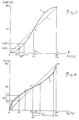
Lorsqu'on effectue le relevé de la tension efficace délivrée sur une résistance fixe en fonction de l'angle de conduction de l'interrupteur commandé pour chaque demi-alternance, on constate (et c'est là la conséquence de la forme sinusoïdale de la tension d'alimentation) que cette tension efficace suit une loi non linéaire en fonction de l'angle de conduction (cf. figure courbe S). Ce phénomène bien connu est très gênant, car toute commande de gradateur en angle de conduction proportionnel à la tension de commande donne une tension de sortie efficace non représentative de la progressivité de la commande. En particulier, l'effet de la commande est très faible en début et en fin de plage de variation, alors qu'il est relativement brutal en milieu de course. Ce défaut est particulièrement gênant dans le cas où l'utilisateur désire une proportionalité quasi parfaite entre la grandeur de commande et la tension efficace de sortie (commande d'éclairage en particulier).When the effective voltage delivered on a fixed resistor is read as a function of the conduction angle of the controlled switch for each half-wave, we see (and this is the consequence of the sinusoidal form of the supply voltage) that this effective voltage follows a nonlinear law as a function of the conduction angle (cf. curve figure S). This well-known phenomenon is very troublesome, because any dimmer control in conduction angle proportional to the control voltage gives an effective output voltage which is not representative of the progressiveness of the control. In particular, the effect of the command is very weak at the start and end of the variation range, whereas it is relatively brutal in the middle of the race. This defect is particularly troublesome in the case where the user wishes an almost perfect proportionality between the control quantity and the effective output voltage (lighting control in particular).
Afin de combattre ce défaut et dans le but d'obtenir une bonne linéarité entre la grandeur de commande et la tension efficace de sortie, les différents constructeurs de ce type de matériel ont adopté des dispositifs de linéarisation divers procurant la correction nécessaire. Généralement, les dispositifs connus utilisent une source de courant variant au cours de chaque demi-alternance afin de créer une rampe de tension non linéaire en fonction du temps (correction dynamique). Cette rampe de tension a une caractéristique de forme voisine de celle de la variation de la tension efficace en fonction de l'angle de conduction et permet ainsi, à l'aide d'un comparateur, d'obtenir une variation de la tension efficace de sortie linéaire par rapport à la grandeur de commande (cf. figure 3, droite L).In order to combat this defect and in order to obtain good linearity between the control quantity and the effective output voltage, the various manufacturers of this type of equipment have adopted various linearization devices providing the necessary correction. Generally, known devices use a current source varying during each half-wave in order to create a non-linear voltage ramp as a function of time (dynamic correction). This voltage ramp has a characteristic shape similar to that of the variation of the effective voltage as a function of the conduction angle and thus makes it possible, using a comparator, to obtain a variation of the effective voltage of linear output with respect to the control variable (see figure 3, right L).
De tels dispositifs à correction dynamique, connus par exemple par les documents DE-A-2 032 949 et US-A-3 942 041, donnent un excellent résultat à la condition de disposer d'une tension d'alimentation parfaitement sinusoïdale et stable en amplitude. Par contre, si l'une de ces condi- tions n'est pas remplie, ce qui est le cas le plus commun pour les réseaux de distribution électrique, la commande de la source à courant variable (généralement réalisée à partir de la tension d'alimentation) ne correspond plus à la correction désirée.Such dynamic correction devices, known for example from documents DE-A-2 032 949 and US-A-3 942 041, give an excellent result provided that a supply voltage is perfectly sinusoidal and stable in amplitude. Against by, if one of these conditions t i ons is not fulfilled, which is the most common case for electrical distribution networks, the control of the variable current source (usually made from the supply voltage) no longer corresponds to the desired correction.
Afin de pallier cet inconvénient, certains constructeurs utilisent un dispositif auxiliaire de régulation de la tension d'alimentation afin de fournir aux éléments dynamiques de correction une tension sinusoïdale de référence correspondant aux critères de qualité nécessaires. Ceci n'est toutefois concevable que pour alimenter des groupes de gradateurs, mais n'est pas économiquement valable pour des gradateurs individuels.In order to overcome this drawback, certain manufacturers use an auxiliary device for regulating the supply voltage in order to provide the dynamic correction elements with a reference sinusoidal voltage corresponding to the necessary quality criteria. This is however only conceivable for supplying groups of dimmers, but is not economically valid for individual dimmers.
Dans le but de remédier à ces divers inconvénients, l'invention a pour objet un dispositif de commande ou déclencheur du genre défini au début, dans lequel le déphasage de l'instant de déclenchement de l'interrupteur commandé est créé proportionnellement à la valeur d'un signal continu qui varie avec le signal de commande conformément à ladite loi de correction par l'interme- diaire d'un générateur de fonction.In order to remedy these various drawbacks, the invention relates to a control device or trigger of the kind defined at the start, in which the phase shift of the instant of tripping of the controlled switch is created in proportion to the value d a continuous signal which varies with the control signal in accordance with said law of correction by means of a function generator.
Cette disposition est avantageuse en ce sens que la correction est réalisée indépendamment de la tension de la source d'alimentation alternative (dans sa forme et surtout dans son amplitude), et cela d'une manière statique, c'est-à-dire qu'à une grandeur de commande fixe correspond un signal continu corrigé également fixe, ce qui permet une meilleure maîtrise des phénomènes et une précision accrue.This arrangement is advantageous in that the correction is carried out independently of the voltage of the AC power source (in its form and especially in its amplitude), and this in a static manner, that is to say that 'to a fixed control quantity corresponds a corrected continuous signal also fixed, which allows better control of phenomena and increased precision.
Ledit signal continu est de préférence engendré, à partir du signal de commande, par un générateur de fonction fournissant, grâce à un réseau non linéaire, une approximation par segments rectilignes raccordés de la loi de correction.Said continuous signal is preferably generated, from the control signal, by a function generator providing, thanks to a non-linear network, an approximation by connected rectilinear segments of the correction law.
Dans une forme d'exécution avantageuse, lorsque la courbe représentant la loi de correction comporte deux moitiés symétriques par rapport à un point central, le réseau non linéaire est conçu pour ne fournir l'approximation par segments rectilignes que de l'une des moitiés de ladite courbe, tandis qu'un réseau auxiliaire de commutation associé à ce réseau lui permet de fournir l'approximation de l'une et l'autre des moitiés symétriques. On obtient ainsi une parfaite symétrie de correction de part et d'autre dudit point central.In an advantageous embodiment, when the curve representing the correction law comprises two halves symmetrical with respect to a central point, the non-linear network is designed to provide the approximation by rectilinear segments only of one of the halves of said curve, while an auxiliary switching network associated with this network allows it to provide the approximation of one and the other of the symmetrical halves. A perfect symmetry of correction is thus obtained on either side of said central point.
Le réseau non linéaire peut alors comprendre une section linéaire et une section non linéaire, tandis que seule la section non linéaire est commutée par le réseau auxiliaire, la section linéaire jouant naturellement son rôle, sans commutation dans les deux moitiés de courbe. Ce réseau auxiliaire peut, de façon très simple, être constitué par un pont de quatre redresseurs, entre deux bornes opposées duquel est connectée la section non linéaire du réseau, la section linéaire de ce dernier étant connectée entre les autres bornes opposées du pont, lesquelles constituent les bornes d'entrée et de sortie de l'ensemble formé par le réseau non linéaire et le réseau auxiliaire.The non-linear network can then comprise a linear section and a non-linear section, while only the non-linear section is switched by the auxiliary network, the linear section. naturally playing its role, without switching in the two halves of the curve. This auxiliary network can, very simply, be constituted by a bridge of four rectifiers, between two opposite terminals of which is connected the non-linear section of the network, the linear section of the latter being connected between the other opposite terminals of the bridge, which constitute the input and output terminals of the assembly formed by the non-linear network and the auxiliary network.
Un tel réseau non linéaire, éventuellement avec le réseau de commutation associé, peut être mis en oeuvre en tant que l'une des impédances d'entrée d'un amplificateur opérationnel pour former avec son impédance de contre-réaction, constituée par une résistance pure, l'ensemble de correction non linéaire désiré.Such a non-linear network, possibly with the associated switching network, can be implemented as one of the input impedances of an operational amplifier to form with its feedback impedance, constituted by a pure resistance. , the desired nonlinear correction set.
Il convient en outre d'appliquer à l'entrée non inverseuse dudit amplificateur opérationnel une tension continue correspondant au point central de symétrie de la courbe représentant la loi de correction, la valeur de cette tension pouvant être réglable afin d'autoriser un décalage dudit point central.It is also advisable to apply to the non-inverting input of said operational amplifier a direct voltage corresponding to the central point of symmetry of the curve representing the correction law, the value of this voltage being able to be adjustable in order to allow a shift of said point. central.
On peut prévoir en pratique que le réseau non linéaire, avec le réseau de commutation éventuellement associé, constitue un circuit bipolaire réalisé sous forme d'un module interchangeable à deux bornes. Ce mode de réalisation sera particulièrement apprécié par les utilisateurs désirant changer la courbe de correction de leurs gradateurs; ils pourront le faire sans avoir à changer l'ensemble de ces appareils.It can be provided in practice that the non-linear network, with the possibly associated switching network, constitutes a bipolar circuit produced in the form of an interchangeable module with two terminals. This embodiment will be particularly appreciated by users wishing to change the correction curve of their dimmers; they can do this without having to change all of these devices.
D'une manière plus particulière, un dispositif selon l'invention peut comprendre un comparateur qui reçoit d'une part un signal issu d'un générateur de rampes et formé de rampes linéaires successives commençant et finissant en synchronisme avec les demi-alternances de la source d'alimentation et d'autre part le signal continu issu du générateur de fonction, et qui déclenche ainsi, à l'instant où ces deux signaux viennent à égalité, l'amorçage de l'interrupteur électronique commandé.More specifically, a device according to the invention may comprise a comparator which receives on the one hand a signal from a ramp generator and formed by successive linear ramps starting and ending in synchronism with the half-vibrations of the power source and on the other hand the continuous signal coming from the function generator, and which thus triggers, at the moment when these two signals come to equality, the ignition of the controlled electronic switch.
D'autres caractéristiques et avantages de l'invention ressortiront plus clairement de la description qui va suivre, en regard des dessins annexés, d'un exemple de réalisation non limitatif.
- - La figure 1 représente le schéma simplifié d'un gradateur équipé d'un dispositif de commande selon l'invention.
- - La figure 2 illustre le principe de fonctionnement d'un tel gradateur.
- - Les figures 3 et 4 présentent deux graphiques illustrant le mode de correction mis en oeuvre dans le dispositif de la figure 1.
- - La figure 5 est un schéma expliquant le principe d'obtention de la correction.
- - La figure 6 représente le schéma détaillé de l'amplificateur de correction du dispositif de la figure 1.
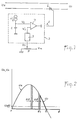
Un gradateur de puissance du genre considéré comprend essentiellement (figure 1) un interrupteur commandé 1 à semi-conducteur et uncircuit 2 de déclenchement de cet interrupteur. L'interrupteur commandé 1 est placé en série avec une source de puissance électrique délivrant une tension alternative Ue (généralement sinusoïdale); il peut s'agir d'un triac, d'une paire de thyristors montés tête-bêche ou éventuellement de tout autre dispositif semi-conducteur à caractéristique de conduction bidirectionnelle équivalente. L'amorçage de l'interrupteur 1 est déclenché par uneimpulsion 1 engendrée par lecircuit 2 à un instant t de phase ϕt variable au cours de chaque demi-période 0 - π de la tension Ue de la source de puissance (figure 2). Il en résulte que chaque demi-afternance de la tension Ue se trouve tronquée, de sorte que la tension de sortie Us, formée de l'ensemble de ces demi-alternances tronquées' présente une valeur efficace Ueff variable en fonction de la phase de l'instant t dans la demi-période. Cette phase est réglable par application d'une tension de commande continue variable Vc au circuit dedéclenchement 2.
- - Figure 1 shows the simplified diagram of a dimmer equipped with a control device according to the invention.
- - Figure 2 illustrates the operating principle of such a dimmer.
- - Figures 3 and 4 show two graphs illustrating the correction mode implemented in the device of Figure 1.
- - Figure 5 is a diagram explaining the principle of obtaining the correction.
- - Figure 6 shows the detailed diagram of the correction amplifier of the device of Figure 1.
A power dimmer of the type under consideration essentially comprises (FIG. 1) a controlledswitch 1 with semiconductor and acircuit 2 for triggering this switch. The controlledswitch 1 is placed in series with an electric power source delivering an alternating voltage Ue (generally sinusoidal); it may be a triac, a pair of thyristors mounted head to tail or possibly any other semiconductor device with equivalent bidirectional conduction characteristic. The ignition of theswitch 1 is triggered by apulse 1 generated by thecircuit 2 at an instant t of phase ϕt variable during each half-period 0 - π of the voltage Ue of the power source (Figure 2) . It follows that each half-alternation of the voltage Ue is truncated, so that the output voltage Us, formed of all of these truncated half-vibrations' has an effective value Ueff variable depending on the phase of l 'instant t in the half period. This phase is adjustable by applying a variable continuous control voltage Vc to thetrigger circuit 2.
Il est clair que la valeur de Ueff n'est pas fonction linéaire de <pt. En effet, comme le montre la figure 2, une même variation Δϕ de la phase de l'instant de déclenchement entraîne une variation de la surface des demi-alternances tronquées de Us qui est plus grande lorsque ledit instant correspond sensiblement au maximum des demi-alternances de Ue. En raison de la forme sinusoïdale de ces dernières, la relation entre Ueff et (pt est d'allure sinusoïdale (figure 3). Lorsque (pt passe de zéro à sa valeur maximale n, Ueff croît d'abord lentement, puis plus vite, puis de nouveau lentement, suivant la courbe S, au lieu de croître li- néairement selon la droite L.It is clear that the value of Ueff is not a linear function of <pt. In fact, as shown in FIG. 2, the same variation Δϕ of the phase of the triggering instant causes a variation in the surface of the truncated half-waves of Us which is greater when said instant corresponds substantially to the maximum of the half-waves. alternations of Ue. Because of the sinusoidal shape of these latter, the relationship between Ueff and (pt is sinusoidal in shape (Figure 3). When (pt goes from zero to its maximum value n, Ueff increases first slowly, then faster, then slowly again, following the curve S, instead of growing linearly along the line L.
Si la phase ϕt de l'instant t est définie proportionnellement à une tension continue V'c, la même courbe S représente les variations de Ueff en fonction de V'c. Dès lors, on voit par exemple qu'une valeur V1 donnée à V'c conduit à une valeur Ueff1 de la valeur efficace de la tension de sortie Us. Pour obtenir la valeur Ueff2 correspondant à une variation linéaire définie par la droite L, il faudrait donner à V'c une valeur V'1 = V1 + ΔV.If the phase ϕt of instant t is defined in proportion to a direct voltage V'c, the same curve S represents the variations of Ueff as a function of V'c. Consequently, we see for example that a value V1 given to V'c leads to a value Ueff1 of the rms value of the output voltage Us. To obtain the value Ueff2 corresponding to a linear variation defined by the line L, it V'c should be given a value V'1 = V1 + ΔV.
Cela signifie qu'en formant, à partir d'une tension de commande Vc, la tension V'c en ajoutant à la tension Vc les quantités AV définies par les écarts d'abscisses existant entre la courbe S et la droite L de la figure 3 pour chaque valeur de Ueff, on obtient une variation de Ueff linéaire et proportionnelle à la valeur de la tension Vc.This means that by forming, from a control voltage Vc, the voltage V'c by adding to the voltage Vc the quantities A V defined by the abscissa differences existing between the curve S and the line L of the FIG. 3 for each value of Ueff, a variation in linear Ueff is obtained which is proportional to the value of the voltage Vc.
La loi de variation de V'c en fonction de Vc, représentée par la courbe S' (figure 4) qui se déduit de la courbe S par une symétrie par rapport à la droite L, est obtenue au moyen d'un générateur de fonction 3. Celui-ci réalise une approximation par segments rectilignes de la courbe S', à l'aide d'un circuit dont le principe est illustré à la figure 5.The law of variation of V'c as a function of Vc, represented by the curve S '(Figure 4) which is deduced from the curve S by a symmetry with respect to the line L, is obtained by means of a
Un amplificateur opérationnel 4, bouclé par une résistance R, comporte une impédance d'entrée formée de trois branches connectées en parallèle, savoir une résistance Ro, une résistan-R1 en série avec un élément à seuil de tension E1, et une résistance R2 en série avec un élément à seuil de tension E2 > E1, ces deux dernières branches formant la section non linéaire de ladite impédance. A l'entrée non inverseuse de l'amplificateur opérationnel 4 est appliquée une tension Vo.An operational amplifier 4, looped by a resistor R, has an input impedance formed by three branches connected in parallel, namely a resistor Ro, a resistance R1 in series with a voltage threshold element E1, and a resistor R2 in series with a voltage threshold element E2> E1, these last two branches forming the non-linear section of said impedance. A voltage Vo is applied to the non-inverting input of the operational amplifier 4.
Quand la tension d'entrée Vc croît à partir d'une valeur égale à Vo, le gain entre la tension de sortie V'c et cette tension Vc est (en valeur absolue) d'abord égal à R/Ro. Puis quand Vc atteint et dépasse la valeur Vo + E1, la résistance R1 se trouve mise en circuit et le gain augmente. Il augmente une nouvelle fois quand la résistance R2 intervient à son tour lorsque Vc devient égal ou supérieur à Vo + E2. On obtient ainsi une loi de variation définie par trois segments rectilignes de pente croissante, qui peuvent fournir une bonne approximation de la partie supérieure de la courbe S' (figure 4) entre le point central X' de celle-ci, correspondant à Vc = Vo, et son point extrême M, atteint lorsque Vc prend sa valeur maximale Vm. 11 est à signaler que le choix des semi-conducteurs déterminant la formation des segments rectilignes successifs est effectué de façon à obtenir des courbes de transition propres à supprimer l'angle de raccordement de ces segments.When the input voltage Vc increases from a value equal to Vo, the gain between the output voltage V'c and this voltage Vc is (in absolute value) first equal to R / Ro. Then when Vc reaches and exceeds the value Vo + E1, the resistor R1 is switched on and the gain increases. It increases again when the resistance R2 intervenes in turn when Vc becomes equal to or greater than Vo + E2. We thus obtain a law of variation defined by three rectilinear segments of increasing slope, which can provide a good approximation of the upper part of the curve S '(Figure 4) between the central point X' thereof, corresponding to Vc = Vo, and its extreme point M, reached when Vc takes its maximum value Vm. It should be noted that the choice of semiconductors determining the formation of successive straight segments is made so as to obtain transition curves capable of eliminating the connection angle of these segments.
Afin d'obtenir également, avec les mêmes éléments, la partie inférieure de la courbe S', symétrique de sa partie supérieure par rapport au point X', on utilise le circuit de la figure 6, qui se déduit de celui de la figure 5 essentiellement par l'adjonction d'un pont de quatre diodes D1, D2, D3, D4 destiné à assurer l'aiguillage de la tension d'entrée Ue de façon qu'elle attaque dans un sens ou dans le sens opposé, suivant que Vc est supérieur ou inférieur à Vo, le bipôle non linéaire formé par les résistances R1 et R2, respectivement en série avec une diode D5 et une diode Zener Z.In order also to obtain, with the same elements, the lower part of the curve S ', symmetrical of its upper part with respect to the point X', the circuit of FIG. 6 is used, which is deduced from that of FIG. 5 essentially by adding a bridge of four diodes D1, D2, D3, D4 intended to ensure the switching of the input voltage Ue so that it attacks in one direction or in the opposite direction, depending on whether Vc is greater or less than Vo, the non-linear bipole formed by the resistors R1 and R2, respectively in series with a diode D5 and a Zener diode Z.
A cet effet, ledit bipôle est connecté entre les extrémités de l'une des diagonales du pont de diodes, tandis que les extrémités de l'autre diagonale, entre lesquelles est connectée la résistance Ro, constituant les bornes d'entrée et de sortie du réseau correcteur 5 ainsi constitué. Dans celui-ci, les tensions E1 et E2 sont respectivement égales à la tension directe de la diode D5 et à la tension de Zener de la diode Z, augmentées de la somme des tensions directes des diodes D1 et D3 ou des diodes D2 et D4 suivant la valeur de Vc par rapport à Vo.To this end, said bipole is connected between the ends of one of the diagonals of the diode bridge, while the ends of the other diagonal, between which the resistance Ro is connected, constituting the input and output terminals of the
Le réseau correcteur 5 constitue l'impédance d'entrée de l'amplificateur opérationnel 4; à ce réseau est appliquée, sous basse impédance via un amplificateur opérationnel 6 bouclé en gain unité, la tension Vc issue par exemple d'un potentiomètre P à variation linéaire (figure 1). Matériellement, le réseau 5 peut se présenter sous la forme d'un module à deux broches de connexion, aisément interchangeable.The
La tension V'c délivrée par le circuit 3 est appliquée à l'une des entrées d'un comparateur 7 dont l'autre entrée reçoit signal Vt en dents de scie linéaires, chacune de celles-ci coïncidant avec une demi-alternance de la tension Ue. Ce signal est engendré par un générateur de courant constant i, de valeur invariable, chargeant un condensateur C qui est décharge périodiquement a chaque passage par zéro de la tension Ue. A chaque fois que le signal en dents de scie franchit un niveau de tension égal à V'c, une impulsion 1 est produite, qui déclenche l'amorçage de l'interrupteur commandé 1. De cette maninère, le déphasage de l'impulsion I dans la demi-alternance correspondante est proportionnel à la tension corrigée V'c, de sorte que la valeur efficace Ueff de la tension de sortie Us du gradateur est constamment proportionnelle à la valeur de la tension continue de commande Vc.The voltage V'c delivered by the
Claims (9)
Applications Claiming Priority (2)
| Application Number | Priority Date | Filing Date | Title |
|---|---|---|---|
| FR8419547A FR2575348B1 (en) | 1984-12-20 | 1984-12-20 | ELECTRONIC DIMMER CONTROL DEVICE |
| FR8419547 | 1984-12-20 |
Publications (2)
| Publication Number | Publication Date |
|---|---|
| EP0186590A1 EP0186590A1 (en) | 1986-07-02 |
| EP0186590B1 true EP0186590B1 (en) | 1990-02-28 |
Family
ID=9310830
Family Applications (1)
| Application Number | Title | Priority Date | Filing Date |
|---|---|---|---|
| EP19850402571 Expired - Lifetime EP0186590B1 (en) | 1984-12-20 | 1985-12-20 | Control device for a phase regulator |
Country Status (3)
| Country | Link |
|---|---|
| EP (1) | EP0186590B1 (en) |
| DE (1) | DE3576253D1 (en) |
| FR (1) | FR2575348B1 (en) |
Family Cites Families (4)
| Publication number | Priority date | Publication date | Assignee | Title |
|---|---|---|---|---|
| FR1348552A (en) * | 1964-04-10 | |||
| GB1288790A (en) * | 1969-12-23 | 1972-09-13 | ||
| US3942041A (en) * | 1973-10-18 | 1976-03-02 | Atmos Corporation | Thyristor control circuit |
| EP0028890A1 (en) * | 1979-11-05 | 1981-05-20 | Westinghouse Electric Corporation | Improved digital gate pulse generator for static power converters |
-
1984
- 1984-12-20 FR FR8419547A patent/FR2575348B1/en not_active Expired
-
1985
- 1985-12-20 DE DE8585402571T patent/DE3576253D1/en not_active Expired - Fee Related
- 1985-12-20 EP EP19850402571 patent/EP0186590B1/en not_active Expired - Lifetime
Also Published As
| Publication number | Publication date |
|---|---|
| FR2575348A1 (en) | 1986-06-27 |
| FR2575348B1 (en) | 1988-02-12 |
| EP0186590A1 (en) | 1986-07-02 |
| DE3576253D1 (en) | 1990-04-05 |
Similar Documents
| Publication | Publication Date | Title |
|---|---|---|
| US4839566A (en) | Circuit for supplying power to a dental photopolymerizing apparatus | |
| EP0496654B1 (en) | Dimmer for a load, with minimal filtering losses | |
| FR2542555A1 (en) | CONTROL CIRCUIT FOR GAS DISCHARGE LAMPS | |
| FR2486348A1 (en) | POWER SUPPLY CIRCUIT FOR A HIGH INTENSITY DISCHARGE LAMP | |
| FR2547688A1 (en) | CALL CURRENT ELIMINATION DEVICE | |
| FR2518329A1 (en) | POWER SUPPLY OF LOW VOLTAGE LOAD | |
| FR2527410A1 (en) | ENHANCED POWER SUPPLY FOR INCANDESCENT LAMP | |
| EP0002981B1 (en) | Method and apparatus for regulating the voltage of an electrical generator | |
| CA1096957A (en) | Two-wire proximity detector | |
| FR2607996A1 (en) | METHOD AND DEVICE FOR IGNITION OF DISCHARGE LAMPS | |
| FR2516335A1 (en) | DEVICE FOR CONTROLLING THE LUMINOUS INTENSITY OF A FLUORESCENT TUBE SUPPLIED ON A CONTINUOUS VOLTAGE | |
| FR2556522A1 (en) | Mains voltage rectifier | |
| EP0065901B1 (en) | Potentiometric transducer system | |
| EP0186590B1 (en) | Control device for a phase regulator | |
| CA2950054A1 (en) | Method and system for light dimmer without flickering on an alternative supply network | |
| EP0967842B1 (en) | Setpoint signal emission on an AC network power line | |
| FR2468527A1 (en) | POWER CONTROL DEVICE FOR TRANSMITTING ENERGY FROM AN ALTERNATING CURRENT SOURCE TO A VIBRANT DISPENSER, AND ASSEMBLY COMPRISING SUCH DEVICE AND DISPENSER | |
| EP0952680B1 (en) | Transmission of an operation mode signal via an AC supply line | |
| FR2563956A1 (en) | INTEGRABLE CIRCUIT FOR SAMPLING THE VOLTAGE OF A LOAD | |
| EP0893875A1 (en) | Storage capacitor charge current adjustment device | |
| EP1120019B1 (en) | Circuit for controlling a load to be supplied by an alternating current voltage | |
| EP0119110B1 (en) | Position detector with a potentiometric sensor, especially for a multidirectional selector | |
| FR2538632A1 (en) | POWER TRANSISTOR CONTROL METHOD AND CIRCUIT | |
| FR2550027A1 (en) | Circuit for phase-angle control of a triac into an inductive load. | |
| FR2526244A1 (en) | Phase controlled voltage AC supply with overvoltage protection - uses circuit, in series with load, comprising rectifier supply switched transistor operated in phase control mode |
Legal Events
| Date | Code | Title | Description |
|---|---|---|---|
| PUAI | Public reference made under article 153(3) epc to a published international application that has entered the european phase |
Free format text: ORIGINAL CODE: 0009012 |
|
| AK | Designated contracting states |
Kind code of ref document: A1 Designated state(s): BE DE LU |
|
| 17P | Request for examination filed |
Effective date: 19861215 |
|
| 17Q | First examination report despatched |
Effective date: 19880426 |
|
| GRAA | (expected) grant |
Free format text: ORIGINAL CODE: 0009210 |
|
| AK | Designated contracting states |
Kind code of ref document: B1 Designated state(s): BE DE LU |
|
| REF | Corresponds to: |
Ref document number: 3576253 Country of ref document: DE Date of ref document: 19900405 |
|
| PLBE | No opposition filed within time limit |
Free format text: ORIGINAL CODE: 0009261 |
|
| STAA | Information on the status of an ep patent application or granted ep patent |
Free format text: STATUS: NO OPPOSITION FILED WITHIN TIME LIMIT |
|
| PGFP | Annual fee paid to national office [announced via postgrant information from national office to epo] |
Ref country code: DE Payment date: 19901224 Year of fee payment: 6 |
|
| PG25 | Lapsed in a contracting state [announced via postgrant information from national office to epo] |
Ref country code: LU Free format text: LAPSE BECAUSE OF NON-PAYMENT OF DUE FEES Effective date: 19901231 Ref country code: BE Effective date: 19901231 |
|
| 26N | No opposition filed | ||
| BERE | Be: lapsed |
Owner name: R.V. ELECTRONIQUE Effective date: 19901231 |
|
| PG25 | Lapsed in a contracting state [announced via postgrant information from national office to epo] |
Ref country code: DE Effective date: 19920901 |