EP0184182A2 - Tubular varistor arrangement - Google Patents
Tubular varistor arrangement Download PDFInfo
- Publication number
- EP0184182A2 EP0184182A2 EP85115302A EP85115302A EP0184182A2 EP 0184182 A2 EP0184182 A2 EP 0184182A2 EP 85115302 A EP85115302 A EP 85115302A EP 85115302 A EP85115302 A EP 85115302A EP 0184182 A2 EP0184182 A2 EP 0184182A2
- Authority
- EP
- European Patent Office
- Prior art keywords
- varistor
- tubular
- arrangement
- sections
- electrically
- Prior art date
- Legal status (The legal status is an assumption and is not a legal conclusion. Google has not performed a legal analysis and makes no representation as to the accuracy of the status listed.)
- Granted
Links
Images
Classifications
-
- H—ELECTRICITY
- H01—ELECTRIC ELEMENTS
- H01C—RESISTORS
- H01C7/00—Non-adjustable resistors formed as one or more layers or coatings; Non-adjustable resistors made from powdered conducting material or powdered semi-conducting material with or without insulating material
- H01C7/10—Non-adjustable resistors formed as one or more layers or coatings; Non-adjustable resistors made from powdered conducting material or powdered semi-conducting material with or without insulating material voltage responsive, i.e. varistors
- H01C7/12—Overvoltage protection resistors; Arresters
-
- H—ELECTRICITY
- H01—ELECTRIC ELEMENTS
- H01R—ELECTRICALLY-CONDUCTIVE CONNECTIONS; STRUCTURAL ASSOCIATIONS OF A PLURALITY OF MUTUALLY-INSULATED ELECTRICAL CONNECTING ELEMENTS; COUPLING DEVICES; CURRENT COLLECTORS
- H01R13/00—Details of coupling devices of the kinds covered by groups H01R12/70 or H01R24/00 - H01R33/00
- H01R13/46—Bases; Cases
- H01R13/53—Bases or cases for heavy duty; Bases or cases for high voltage with means for preventing corona or arcing
Definitions
- the present invention relates to a tubular varistor arrangement, and, more particularly, to a varistor arrangement suitable for use in an electrical connector of circular cross-section.
- an object of the invention is to provide a tubular varistor arrangement that may utilize standard varistor compositions for application in a circular connector subject to a tubular wall thickness-restriction.
- Another object of the invention is to provide a tubular varistor arrangement for application in a tubular wall thickness-restricted electrical connector that can be fabricated without expensive retooling for producing the connector.
- a further object of the invention is to provide a tubular varistor arrangement having a breakdown voltage of several times that of any single tubular varistor of the arrangement.
- the foregoing tubular varistor arrangement attains a breakdown voltage constituting the combined breakdown voltages of the first and the second varistor sections.
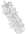
- a tubular varistor arrangement 10 is depicted in the sole.drawing Figure.
- Varistor arrangement 10 includes first and second tubular varistor sections 12 and 14, respectively, aligned with each other along their longitudinal axes.
- a center conductor 16, such as copper, is disposed generally concentrically within varistor sections 12 and 14. Center conductor 16 is preferably coated with electrical insulation 17, such as high dielectric strength paper or heat-shrink polymer.
- a tubular electrode 18 adjoins the radially inner surface of tubular varistor section 12, and a tubular electrode 20 adjoins the radially outer surface of varistor section 12.
- tubular electrodes 22 and 24 adjoin the inner and outer radial surfaces, respectively, of tubular varistor section 14.
- These various tubular electrodes i.e., electrodes 18, 20, 22 and 24
- An intermediate support member 30 is interposed between tubular varistor sections 12 and 14. Support member 30 is spaced from center conductor 16 by insulation layer 17, and may additionally be separated from conductor 16 by an air gap 33.
- inner electrode 18 is electrically shorted to center conductor 16, via conductive support member 26; outer electrode 20 is electrically shorted to inner electrode 22, via conductive support member 30; and outer electrode 24 is electrically shorted to a reference, or ground, potential conductor 36 (illustrated schematically).
- the breakdown voltage of varistor arrangement 10 is effectively twice that of either varistor section 12 or 14. This is because the use of two varistor sections 12 and 14, electrically interconnected as described herein, places the varistors sections in a serial circuit relationship. Accordingly, the respective breakdown voltages of varistor sections 12 and 14, which are proportional to the respective thicknesses T 1 and T 2 of the varistor sections, cumulate to yield the same breakdown voltage as could be provided by a varistor of thickness T 1 + T 2'
- the foregoing describes a varistor arrangement that attains a breakdown voltage of several times that of a single tubular varistor of the arrangement.
- the varistor arrangement is particularly beneficial in presently-available electrical connectors of circular cross-section, in which varistor material of standard composition may be used without altering the dimensions of the electrical connectors.
Landscapes
- Engineering & Computer Science (AREA)
- Microelectronics & Electronic Packaging (AREA)
- Physics & Mathematics (AREA)
- Electromagnetism (AREA)
- Thermistors And Varistors (AREA)
Abstract
Description
- The present invention relates to a tubular varistor arrangement, and, more particularly, to a varistor arrangement suitable for use in an electrical connector of circular cross-section.
- Presently-available electrical connectors that are circular in cross-section are typically restricted in the wall thickness of tubular electrical circuit elements which can be integrated into the connectors. This is a result of the considerable capital costs associated with design and acquisition of the various machine tools required to produce a circular connector. Various power and signal level electrical systems incorporating circular connectors, however, require respective varistor breakdown voltages that are incompatible with tubular varistors of presently-available compositions subject to a typical restriction on tubular wall thickness. This is because varistor breakdown voltage varies according to the thickness of varistor material between a pair of spaced electrodes. While it would be possible to comply with the foregoing tubular wall thickness-restriction by formulating varistor compositions of desired breakdown voltage for a specified wall thickness, it would be desirable to utilize presently-available varistor compositions, since these have been exhaustively optimized in regard to a comprehensive range of performance parameters.
- Accordingly, an object of the invention is to provide a tubular varistor arrangement that may utilize standard varistor compositions for application in a circular connector subject to a tubular wall thickness-restriction.
- Another object of the invention is to provide a tubular varistor arrangement for application in a tubular wall thickness-restricted electrical connector that can be fabricated without expensive retooling for producing the connector.
- A further object of the invention is to provide a tubular varistor arrangement having a breakdown voltage of several times that of any single tubular varistor of the arrangement.
- The foregoing and further objects of the invention are realized, in preferred form, in a tubular varistor arrangement comprising first and second tubular varistor sections aligned with each other. A center conductor is disposed generally concentrically within the first and second varistor sections. First and second tubular electrodes adjoin the inner and outer radial surfaces, respectively, of the first varistor section, while third and fourth tubular electrodes adjoin the inner and outer radial surfaces, respectively, of the second varistor section. The first tubular electrode is electrically shorted to the center conductor; the second tubular electrode is electrically shorted to the third tubular electrode, while being electrically isolated from the center electrode; and the fourth tubular electrode is electrically shorted to a reference potential conductor.
- The foregoing tubular varistor arrangement attains a breakdown voltage constituting the combined breakdown voltages of the first and the second varistor sections.
- While the specification concludes with claims defining the features of the invention regarded as novel, the invention itself, as to both organization and method of operation, will be better understood from the following description, in conjunction with the sole drawing figure, depicting a tridimensional view of a preferred tubular varistor arrangement, a portion of the arrangement being cut away to illustrate more clearly details of the present invention.
- A
tubular varistor arrangement 10 is depicted in the sole.drawing Figure.Varistor arrangement 10 includes first and secondtubular varistor sections varistor sections - A
tubular electrode 18 adjoins the radially inner surface oftubular varistor section 12, and atubular electrode 20 adjoins the radially outer surface ofvaristor section 12. Similarly,tubular electrodes tubular varistor section 14. These various tubular electrodes (i.e.,electrodes varistor sections -
Varistor sections support members Support member 26 includes an aperture 26A, in which center conductor 16 is rigidly disposed.Support member 26 further includes a tubular flange 26B onto which the radially inner surface ofvaristor 12 is mechanically supported viatubular electrode 18. As withsupport member 26,support member 28 includes an aperture 28A, into which insulation-coated center conductor 16 is rigidly disposed.Support member 26 further includes a tubular flange 26B, onto which the radially inner surface ofthyristor section 14 is affixed. - An
intermediate support member 30 is interposed betweentubular varistor sections Support member 30 is spaced from center conductor 16 by insulation layer 17, and may additionally be separated from conductor 16 by anair gap 33. -
Support members Support member 28 comprises an electrically-insulating material; for example, an elastomer of silicone. - To achieve the desired breakdown voltage for
tubular varistor assembly 10,inner electrode 18 is electrically shorted to center conductor 16, viaconductive support member 26;outer electrode 20 is electrically shorted toinner electrode 22, viaconductive support member 30; andouter electrode 24 is electrically shorted to a reference, or ground, potential conductor 36 (illustrated schematically). - The breakdown voltage of
varistor arrangement 10 is effectively twice that of eithervaristor section varistor sections varistor sections - The foregoing describes a varistor arrangement that attains a breakdown voltage of several times that of a single tubular varistor of the arrangement. The varistor arrangement is particularly beneficial in presently-available electrical connectors of circular cross-section, in which varistor material of standard composition may be used without altering the dimensions of the electrical connectors.
- While the invention has been described with respect to specific embodiments by way of illustration, many modifications and changes will occur to those skilled in the art. For example, more than two varistor sections could be employed in a tubular varistor arrangement to achieve a commensurate increase in total breakdown voltage. Additionally, various parts described herein as being "tubular" need not be perfectly tubular in configuration; accordingly, for instance, a tubular electrode may only partially circumscribe a varistor section. It is, therefore, to be understood that the appended claims are intended to cover all such modifications and changes as fall within the true spirit and scope of the invention.
Claims (5)
Applications Claiming Priority (2)
| Application Number | Priority Date | Filing Date | Title |
|---|---|---|---|
| US678726 | 1984-12-05 | ||
| US06/678,726 US4638284A (en) | 1984-12-05 | 1984-12-05 | Tubular varistor arrangement |
Publications (3)
| Publication Number | Publication Date |
|---|---|
| EP0184182A2 true EP0184182A2 (en) | 1986-06-11 |
| EP0184182A3 EP0184182A3 (en) | 1987-01-14 |
| EP0184182B1 EP0184182B1 (en) | 1989-07-26 |
Family
ID=24723998
Family Applications (1)
| Application Number | Title | Priority Date | Filing Date |
|---|---|---|---|
| EP85115302A Expired EP0184182B1 (en) | 1984-12-05 | 1985-12-03 | Tubular varistor arrangement |
Country Status (4)
| Country | Link |
|---|---|
| US (1) | US4638284A (en) |
| EP (1) | EP0184182B1 (en) |
| JP (1) | JPS61142702A (en) |
| DE (1) | DE3571890D1 (en) |
Cited By (6)
| Publication number | Priority date | Publication date | Assignee | Title |
|---|---|---|---|---|
| WO1991011040A1 (en) * | 1990-01-09 | 1991-07-25 | Raychem Gmbh | Cable connector |
| GB2242067A (en) * | 1990-03-16 | 1991-09-18 | Ecco Ltd | Varistors |
| US5837178A (en) * | 1990-03-16 | 1998-11-17 | Ecco Limited | Method of manufacturing varistor precursors |
| US6183685B1 (en) | 1990-06-26 | 2001-02-06 | Littlefuse Inc. | Varistor manufacturing method |
| US6334964B1 (en) | 1990-03-16 | 2002-01-01 | Littelfuse, Inc. | Varistor ink formulations |
| EP2889882A4 (en) * | 2013-03-08 | 2015-12-30 | Long Ke Electronics Hui Yang Co Ltd | TUBULAR RESISTANCE DEPENDENT ON VOLTAGE |
Families Citing this family (26)
| Publication number | Priority date | Publication date | Assignee | Title |
|---|---|---|---|---|
| US4908597A (en) * | 1987-04-28 | 1990-03-13 | Christopher Sutton | Circuit module for multi-pin connector |
| JPS63299714A (en) * | 1987-05-28 | 1988-12-07 | Matsushita Electric Ind Co Ltd | surge noise absorber |
| JPS63299718A (en) * | 1987-05-28 | 1988-12-07 | Matsushita Electric Ind Co Ltd | surge noise absorber |
| JP2595538B2 (en) * | 1987-05-28 | 1997-04-02 | 松下電器産業株式会社 | Surge noise absorber |
| JPS63299712A (en) * | 1987-05-28 | 1988-12-07 | Matsushita Electric Ind Co Ltd | surge noise absorber |
| JP2600172B2 (en) * | 1987-05-28 | 1997-04-16 | 松下電器産業株式会社 | Surge noise absorber |
| DE19701243A1 (en) * | 1997-01-16 | 1998-07-23 | Asea Brown Boveri | Column-shaped, high-current-resistant resistor, in particular varistor based on a metal oxide, and method for producing such a resistor |
| CN101331562B (en) * | 2005-10-19 | 2011-06-01 | 东莞令特电子有限公司 | A varistor and production method |
| WO2008035319A1 (en) * | 2006-09-19 | 2008-03-27 | Littelfuse Ireland Development Company Limited | Manufacture of varistors comprising a passivation layer |
| SI23462B (en) * | 2010-08-26 | 2015-06-30 | Eti Elektroelement D.D. | Varistor fuse |
| US9431158B2 (en) * | 2014-08-19 | 2016-08-30 | Longke Electronics (Huiyang) Co., Ltd. | Barrel-shaped fireproof and explosion-proof surge protection device with over-temperature protection function |
| GB2546492A (en) * | 2016-01-19 | 2017-07-26 | Mpe Ip Ltd | Varistors |
| US10319545B2 (en) | 2016-11-30 | 2019-06-11 | Iskra Za{hacek over (s)}{hacek over (c)}ite d.o.o. | Surge protective device modules and DIN rail device systems including same |
| US10707678B2 (en) | 2016-12-23 | 2020-07-07 | Ripd Research And Ip Development Ltd. | Overvoltage protection device including multiple varistor wafers |
| US10447026B2 (en) | 2016-12-23 | 2019-10-15 | Ripd Ip Development Ltd | Devices for active overvoltage protection |
| US10340110B2 (en) | 2017-05-12 | 2019-07-02 | Raycap IP Development Ltd | Surge protective device modules including integral thermal disconnect mechanisms and methods including same |
| US10685767B2 (en) | 2017-09-14 | 2020-06-16 | Raycap IP Development Ltd | Surge protective device modules and systems including same |
| US11223200B2 (en) | 2018-07-26 | 2022-01-11 | Ripd Ip Development Ltd | Surge protective devices, circuits, modules and systems including same |
| US11862967B2 (en) | 2021-09-13 | 2024-01-02 | Raycap, S.A. | Surge protective device assembly modules |
| US11723145B2 (en) | 2021-09-20 | 2023-08-08 | Raycap IP Development Ltd | PCB-mountable surge protective device modules and SPD circuit systems and methods including same |
| US11990745B2 (en) | 2022-01-12 | 2024-05-21 | Raycap IP Development Ltd | Methods and systems for remote monitoring of surge protective devices |
| US12506334B2 (en) | 2022-01-24 | 2025-12-23 | Raycap IP Development Ltd | Surge protective device modules and assemblies |
| US12199412B2 (en) | 2022-06-02 | 2025-01-14 | Ripd Ip Development Ltd. | Surge protective devices, circuits, modules and systems including same |
| US12206234B2 (en) | 2022-09-20 | 2025-01-21 | Ripd Ip Development Ltd | Overvoltage protection device modules |
| US12437906B2 (en) | 2022-10-18 | 2025-10-07 | Raycap, S.A. | Surge protective devices |
| US12580381B2 (en) | 2023-12-04 | 2026-03-17 | Ripd Ip Development Ltd | Overvoltage protection device modules and sheath bonding systems including same |
Family Cites Families (9)
| Publication number | Priority date | Publication date | Assignee | Title |
|---|---|---|---|---|
| US857849A (en) * | 1904-10-20 | 1907-06-25 | Electric Service Supplies Co | Lightning-arrester. |
| US1063303A (en) * | 1909-07-13 | 1913-06-03 | Gen Electric | Electrical resistance. |
| US3227983A (en) * | 1963-08-07 | 1966-01-04 | Air Reduction | Stacked resistor |
| DE6609456U (en) * | 1966-09-28 | 1972-05-25 | Lorraine Carbone | ADJUSTABLE FILM RESISTANCE. |
| US3711794A (en) * | 1971-10-21 | 1973-01-16 | Gen Electric | Surge suppression transmission means |
| US4335417A (en) * | 1978-09-05 | 1982-06-15 | General Electric Company | Heat sink thermal transfer system for zinc oxide varistors |
| US4276578A (en) * | 1979-05-10 | 1981-06-30 | General Electric Company | Arrester with graded capacitance varistors |
| US4352139A (en) * | 1980-02-04 | 1982-09-28 | Rte Corporation | Flexible connector for H.V. arrester |
| CH659550A5 (en) * | 1983-03-21 | 1987-01-30 | Bbc Brown Boveri & Cie | VOLTAGE-LIMITING PROCEDURE. |
-
1984
- 1984-12-05 US US06/678,726 patent/US4638284A/en not_active Expired - Lifetime
-
1985
- 1985-12-03 DE DE8585115302T patent/DE3571890D1/en not_active Expired
- 1985-12-03 JP JP60270864A patent/JPS61142702A/en active Granted
- 1985-12-03 EP EP85115302A patent/EP0184182B1/en not_active Expired
Cited By (7)
| Publication number | Priority date | Publication date | Assignee | Title |
|---|---|---|---|---|
| WO1991011040A1 (en) * | 1990-01-09 | 1991-07-25 | Raychem Gmbh | Cable connector |
| GB2242067A (en) * | 1990-03-16 | 1991-09-18 | Ecco Ltd | Varistors |
| GB2242067B (en) * | 1990-03-16 | 1994-05-04 | Ecco Ltd | Varistor configurations |
| US5837178A (en) * | 1990-03-16 | 1998-11-17 | Ecco Limited | Method of manufacturing varistor precursors |
| US6334964B1 (en) | 1990-03-16 | 2002-01-01 | Littelfuse, Inc. | Varistor ink formulations |
| US6183685B1 (en) | 1990-06-26 | 2001-02-06 | Littlefuse Inc. | Varistor manufacturing method |
| EP2889882A4 (en) * | 2013-03-08 | 2015-12-30 | Long Ke Electronics Hui Yang Co Ltd | TUBULAR RESISTANCE DEPENDENT ON VOLTAGE |
Also Published As
| Publication number | Publication date |
|---|---|
| EP0184182A3 (en) | 1987-01-14 |
| EP0184182B1 (en) | 1989-07-26 |
| JPH0250606B2 (en) | 1990-11-02 |
| US4638284A (en) | 1987-01-20 |
| JPS61142702A (en) | 1986-06-30 |
| DE3571890D1 (en) | 1989-08-31 |
Similar Documents
| Publication | Publication Date | Title |
|---|---|---|
| EP0184182B1 (en) | Tubular varistor arrangement | |
| US4198613A (en) | Filter contact | |
| CA1138538A (en) | Filter connector with compound filter elements | |
| CA1117194A (en) | Discoidal monolithic ceramic capacitor | |
| US4952173A (en) | Circuit protection device | |
| US4747789A (en) | Filter electrical connector with transient suppression | |
| US11378594B2 (en) | Capacitive voltage sensor with hidden sensing electrode | |
| US4620074A (en) | Contact arrangement for vacuum switches | |
| US7388737B2 (en) | Multilayer capacitor and method of adjusting equivalent series resistance of multilayer capacitor | |
| US11683880B2 (en) | Encapsulated printed circuit board assembly | |
| US3659033A (en) | Electrical bushing having adjacent capacitor sections separated by axially continuous conductive layers, and including a cooling duct | |
| GB1385258A (en) | Transmission line section | |
| EP0551740A1 (en) | A miniature electric motor with a spark-quenching element | |
| US3646251A (en) | Electrical bushing having stress-grading layer disposed within solid insulation including a ground layer term inated at each end with a layer of material having a voltage-dependent resistivity | |
| US3462545A (en) | Condenser bushing | |
| CN108321649B (en) | Multifunctional combined rotary connector and assembling method thereof | |
| US6767217B2 (en) | Rotating electrical transfer components | |
| US3302082A (en) | High-voltage capacitor of low inductance | |
| WO2008027007A1 (en) | High voltage dc bushing and device comprising such high voltage bushing | |
| US4491713A (en) | Power and sensing cable arrangement for electrical discharge machining assembly | |
| US6396678B1 (en) | Capacitor | |
| US3248619A (en) | Metallized-electrode capacitor construction | |
| US4403104A (en) | Gas-insulated bushing having minimized throat diameter | |
| US3793477A (en) | Condenser bushing having displaced gaps between conducting layers | |
| JPH03222621A (en) | Gas-insulated spacer |
Legal Events
| Date | Code | Title | Description |
|---|---|---|---|
| PUAI | Public reference made under article 153(3) epc to a published international application that has entered the european phase |
Free format text: ORIGINAL CODE: 0009012 |
|
| AK | Designated contracting states |
Kind code of ref document: A2 Designated state(s): DE FR GB NL |
|
| PUAL | Search report despatched |
Free format text: ORIGINAL CODE: 0009013 |
|
| AK | Designated contracting states |
Kind code of ref document: A3 Designated state(s): DE FR GB NL |
|
| 17P | Request for examination filed |
Effective date: 19870708 |
|
| 17Q | First examination report despatched |
Effective date: 19881102 |
|
| GRAA | (expected) grant |
Free format text: ORIGINAL CODE: 0009210 |
|
| AK | Designated contracting states |
Kind code of ref document: B1 Designated state(s): DE FR GB NL |
|
| REF | Corresponds to: |
Ref document number: 3571890 Country of ref document: DE Date of ref document: 19890831 |
|
| ET | Fr: translation filed | ||
| PLBE | No opposition filed within time limit |
Free format text: ORIGINAL CODE: 0009261 |
|
| STAA | Information on the status of an ep patent application or granted ep patent |
Free format text: STATUS: NO OPPOSITION FILED WITHIN TIME LIMIT |
|
| 26N | No opposition filed | ||
| PGFP | Annual fee paid to national office [announced via postgrant information from national office to epo] |
Ref country code: FR Payment date: 19991117 Year of fee payment: 15 |
|
| PGFP | Annual fee paid to national office [announced via postgrant information from national office to epo] |
Ref country code: GB Payment date: 19991118 Year of fee payment: 15 Ref country code: DE Payment date: 19991118 Year of fee payment: 15 |
|
| PGFP | Annual fee paid to national office [announced via postgrant information from national office to epo] |
Ref country code: NL Payment date: 19991122 Year of fee payment: 15 |
|
| PG25 | Lapsed in a contracting state [announced via postgrant information from national office to epo] |
Ref country code: GB Free format text: LAPSE BECAUSE OF NON-PAYMENT OF DUE FEES Effective date: 20001203 |
|
| PG25 | Lapsed in a contracting state [announced via postgrant information from national office to epo] |
Ref country code: NL Free format text: LAPSE BECAUSE OF NON-PAYMENT OF DUE FEES Effective date: 20010701 |
|
| GBPC | Gb: european patent ceased through non-payment of renewal fee |
Effective date: 20001203 |
|
| PG25 | Lapsed in a contracting state [announced via postgrant information from national office to epo] |
Ref country code: FR Free format text: LAPSE BECAUSE OF NON-PAYMENT OF DUE FEES Effective date: 20010831 |
|
| NLV4 | Nl: lapsed or anulled due to non-payment of the annual fee |
Effective date: 20010701 |
|
| REG | Reference to a national code |
Ref country code: FR Ref legal event code: ST |
|
| PG25 | Lapsed in a contracting state [announced via postgrant information from national office to epo] |
Ref country code: DE Free format text: LAPSE BECAUSE OF NON-PAYMENT OF DUE FEES Effective date: 20011002 |