EP0183565A1 - Method and apparatus for checking articles against a standard - Google Patents
Method and apparatus for checking articles against a standard Download PDFInfo
- Publication number
- EP0183565A1 EP0183565A1 EP85308723A EP85308723A EP0183565A1 EP 0183565 A1 EP0183565 A1 EP 0183565A1 EP 85308723 A EP85308723 A EP 85308723A EP 85308723 A EP85308723 A EP 85308723A EP 0183565 A1 EP0183565 A1 EP 0183565A1
- Authority
- EP
- European Patent Office
- Prior art keywords
- article
- articles
- standard
- image
- dimensions
- Prior art date
- Legal status (The legal status is an assumption and is not a legal conclusion. Google has not performed a legal analysis and makes no representation as to the accuracy of the status listed.)
- Withdrawn
Links
Images


Classifications
-
- G—PHYSICS
- G06—COMPUTING; CALCULATING OR COUNTING
- G06T—IMAGE DATA PROCESSING OR GENERATION, IN GENERAL
- G06T7/00—Image analysis
- G06T7/0002—Inspection of images, e.g. flaw detection
- G06T7/0004—Industrial image inspection
- G06T7/001—Industrial image inspection using an image reference approach
-
- G—PHYSICS
- G01—MEASURING; TESTING
- G01B—MEASURING LENGTH, THICKNESS OR SIMILAR LINEAR DIMENSIONS; MEASURING ANGLES; MEASURING AREAS; MEASURING IRREGULARITIES OF SURFACES OR CONTOURS
- G01B11/00—Measuring arrangements characterised by the use of optical techniques
- G01B11/02—Measuring arrangements characterised by the use of optical techniques for measuring length, width or thickness
- G01B11/024—Measuring arrangements characterised by the use of optical techniques for measuring length, width or thickness by means of diode-array scanning
-
- G—PHYSICS
- G06—COMPUTING; CALCULATING OR COUNTING
- G06T—IMAGE DATA PROCESSING OR GENERATION, IN GENERAL
- G06T2207/00—Indexing scheme for image analysis or image enhancement
- G06T2207/30—Subject of image; Context of image processing
- G06T2207/30108—Industrial image inspection
- G06T2207/30164—Workpiece; Machine component
Definitions
- This invention relates to a method and apparatus for checking articles against a standard.
- an article to be checked is illuminated with a light beam from a source such as a laser or an incandescent or strobe lamp, and the light reflected from the article detected on a photodetector such as a television-type detector device, a vidicon, an array of photosensitive elements or a photomultiplier tube.
- a source such as a laser or an incandescent or strobe lamp
- a photodetector such as a television-type detector device, a vidicon, an array of photosensitive elements or a photomultiplier tube.
- the detected light from the article provides information about parameters of the article, which can be compared with standard values in order to determine conformity of the article with a standard.
- US-A-4111557 there is disclosed a method for optical determination and comparison of shapes, in which a line or point of light is projected onto an article by a source.
- the reflected rays are received by a TV camera or a photodiode matrix.
- the image signals are converted to digital data which is passed to a computer unit having storage.
- the stored values are compared with standard values to determine their difference from the standard.
- the resulting data is output from the computer to a plotter and/or a monitor.
- US-A-441456 discloses a sorting and inpspection apparatus which digitizes a TV camera output. The digitized output is stored and compared with a previously stored image which was recorded by placing a standard article in front of the TV camera.
- US-A-4343553 discloses a split or line projector with two image detectors positioned at 45° for testing the shape and height of a soldered joint. The resulting video signal is compared with first and second references to determine whether the joint is over soldered, under soldered, or acceptable.
- US-A-4105925 discloses an optical article locator with a left and a right light source each emitting light in a sheet at an acute angle to a conveyor belt surface.
- a linear diode array is positioned above the conveyor belt between the two light sources and is narrowly focused on a line of light formed at the intersection of the two sheets of light.
- the output from the linear diode array is provided to a programmed computer or microprocessor in a control unit for determining the position and orientation of articles on the conveyor belt passing through the field of view.
- US-A-3,667,846 discloses an optical surface inpection apparatus for detecting microscopic variations in a surface area and producing signals which are compared with the signals of a predetermined reference surface.
- a light source projects a spot of light onto the surface from an angle and the reflected light is sensed by an optical detector also set at an angle to the surface.
- US-A-3,796,492 discloses a laser dimension comparator in which two beams of light are set at an angle to the surface being evaluated and reflected to a vidicon whose output signals are processed and digitized. The measured dimension is then displayed on a digital display.
- a reference surface is positioned at a fixed distance from a gauging head on the vidicon to obtain a reference surface which is stored in a comparator circuit for subsequent comparison to actual work pieces.
- US-A-3,791,741 discloses a size gauging and quality-inspecting apparatus in which articles are inspected in two successive inspection stations. The items are illuminated and the reflected light is detected by an optical sensor. The modulated light is electronically measured to produce signals corresponding to dimensions which are compared to a predetermined standard.
- US-A-4,311,392 discloses a thickness measuring apparatus with a light projector and an optical detector set at 45° to the surface of a sheet being evaluated.
- a processing mechanism calculates the thickness of the sheet based on the relative surface positions of the sheet and a metal roll over which the sheet is moved.
- US-A-4,139,304 discloses measuring variations in distance to a surface and determining surface contours using spaced-apart projected sheets of light which intersect the surface and a photodetector which receives the reflected light at an angle.
- US-A-4,146,926 discloses a method and apparatus for optically exploring the surface of an article in which a laser beam is scanned over the surface. Reflected light beams are received by a TV camera. The output signals from the TV camera are used by a computer to determine the contour and height dimension of a point on the surface of the article.
- US-A-4,279,513 discloses an optical, electronic measurement system which scans and images only the edges of a work piece.
- the measurement system is initially calibrated by positioning a work piece of known dimensions in the field of view; storing the signals representative of the standard of known work piece; and comparing similar work pieces of unknown dimensions to the standard.
- a method of checking an article for conformity thereof with a standard in which the article is illuminated with incident light and light reflected from the article is detected with a detector device which converts the detected light into electrical signals which are compared with signals representative of a standard article using a computer, characterised in that the detector device is a photosensitive random access memory device which is read directly by the computer to obtain said electrical signals.
- the method is characterised by the steps of moving a succession of articles; projecting incident light in at least one single line to the succession of articles and applying the line of light successively to the moving articles to illuminate each article with said light; detecting with the photosensitive random access memory the incidence of said line of light at said articles; operating a system computer comparator in response to inputs representing the detected light to produce information about the dimensions of each article in the photosensitive random access memory; retaining and storing said information in a separate random access memory; storing information of a standard value of the dimensions of each article in said separate random access memory; determining the information of each article on said photosensitive random access memory; transferring the data directly to the separate random access memory in digital form; and comparing the information on the standard image and each article.
- a method of checking articles for conformity of a parameter thereof with a standard parameter value the parameter being measured optically and compared with the standard parameter value using a computer, characterised in that the standard parameter is derived from a plurality of parameter measurements carried out on a plurality of articles
- apparatus for inspecting by illumination a succession of articles to detect physical characteristics as compared to a standard and making a determination of conformance with the standard, characterized by dimension-detecting apparatus providing digital signals obtained by scanning an image optically produced on a photosensitive random access memory from an article and.detecting an abnormal state of the dimension of said article so as to classify the article, said dimension detecting apparatus comprising means sensing and measuring a series of standard articles; means for producing a model means characteristic of an article with dimensions within the range of a predetermined deviation; and means for scanning the image output, of sensing and measuring each image optically produced from an article and for detecting the dimensions of each article so as to classify each article.
- the system of writing computer instructions and statements for a program has as its ultimate objective an application of the program which results in the selection and approval of articles within the range of the determined average deviation. Also defective articles are identified and the nature of the defects noted and collated.
- the comparison discovers a significant difference between an inspected article and the standard, the inspected article is selected for rejection, and the amount of deviation may be noted and used for trend analysis.
- the optical system involves a beam of light in a single line or grid pattern directed at and incident on the articles which may be moving on a conveyor system and transversely across the articles.
- the beam of light is directed at the plane at an angle of 45°. It is an advantage that the setting of the angle of 45° causes the object to create a break in the line of light into two separate lines. The distance of the separation between these lines is equal to the height of the bar. This break in the lines is detected and transferred to the photosensitive memory.
- a dynamic memory integrated circuit chip is used as memory for a microprocessor and by permitting light to strike the die when the refresh is off, the same device becomes a photosensitive detector array for optical images. The use of this technique eliminates the need for a television camera, or working with a whole image or an analog to digital converter or the computer image processing time required to produce a binary image suitable for standard measuring algorithms.
- the image that is produced on the photosensitive memory by the standard is comprised of a large number of memory cells of the memory.
- specific critical cells are identified as representing the body of the article. Further of these specifically identified cells, there are cells which are identified as located with transition points (edges) in the image of the article.
- These cells at the transition points in the present embodiment contain data in the form of bits, a loss, or lack of charge or a logic "0". This information through the action of the program in the processing units is transmitted in bit form to the storage memory where it is stored as an address table.
- a significant aspect in the imaging, detection and transmission procedure involving the photosensitive dynamic memory lies in the speed provided which in turn has a faster refresh signal to maintain the image.
- This refresh signal proceeding every 1/8 millisecond through the memory keeps the data available for read out. Because of this high speed the refreshing preserves uniform exposure of the images on the memory.
- the program signals locate and detect the cell having the data. This data is then read out of the photosensitive memory to the storage memory where the correct points are stored.
- Fig. 1 shows an embodiment of a measuring apparatus for bodies.
- An optical system 10 is comprised of an object lens 13, and a source of light 11, and a condenser lens 12 which project a light beam 14 in a pattern at and incident on an object 15.
- the object 15 may be in motion on a conveyor system not shown and the light beam is directed and incident on the object transversely accross the object.
- the beam of light 14 is directed at a plane of the object at an angle of 45° and the setting of the angle of 45° causes the object to create a break of the line of the light beam into two separate lines. This distance of the separation of these lines is proportional to the height of the object.
- the light beam and the break in the line is transferred and directed to a photosensitive RAM 16.
- the RAM 16 is an integrated circuit that linearly converts light level into electrical current. It is designed as an imaging device made of memory cells. In one preferred embodiment the memory cells are arranged in a regular pattern of 256 elements in a row by 128 elements in a column. This embodiment provides 32,768 discrete imaging locations.
- the RAM 16 is a memory in conjunction with a system 17.
- the RAM 16 acts as a detection mechanism to be described further below.
- the system 17 includes a CPU (central processing unit) 18, a RAM 19, which are interconnected and connected to the optic RAM 16 by a data bus 20.
- the CPU 18 is connected also by a control bus 21 and an address bus 22.
- An EPROM unit 23 is connected by the data bus 20 and the address bus 22.
- the EPROM interconnects with the CPU 18 by bus 24 and with storage RAM 19 by bus 25.
- the image analysis with the necessary computer operations is processed in the electronic hardware of system 17.
- the image of the object 15 as viewed by the system 10 is retained on the photosensitive dynamic RAM 16 and is involved in the processing which is described further hereinafter.
- each of a succession of objects 15 are removed and replaced successively in the optical system 10.
- a feature of an inspection procedure according to this invention is that checking the inspected objects in practice involves reading only critical points of the retained image on photosensitive RAM 16. It is the critical dimensions of the inspected objects 15 that are detected and stored in the memory of RAM 19. Then these detected and stored dimensions are compared with standard dimensions of the object 15 stored in RAM 19. In this way deviations that may occur in the successive inspected objects 15 are detected.
- the EPROM 23 provides the programming of the initial analysis and the detection comparison, decisions and subsequent action.
- the photosensitive RAM 16 is a memory related to the system 17 and acts as a detection mechanism.
- the memory cells in the array can be randomly accessed. This is done by row and column address strobes. As explained below, the row address strobe first addresses a row in which a cell to be accessed is present and then the column address strobe addresses the column of the particular memory cell. The confluence of these row and address strobe makes the data available on the particular cell.
- Fig. 2 is an illustrative circuit diagram of a memory cell 30 of the RAM 16.
- the cell 30 contains a photosenstive element 31 illustrated in Fig. 2 as an n-channel unijunction transistor.
- the memory cell 30 is a single transistor dynamic cell.
- the element 31 controls access to the storage capacitor 29.
- the capacitance of capacitor 29 exists between the drain of the element 31 and ground. The other contact to the drain is connected to a column of the RAM 16 array and the gate is connected to a row
- Each memory cell 30 is precharged to a fixed voltage of +5 volts. These individual cells after this charging to 5 volts are discharged by light incident on the photosensitive element 31. In Fi G 2, the incident light is represented by the broken arrow falling on the element 31.
- the capacitor 29 charged to +5 volts is discharged as the element 31 photosensitivity cause a flow of current through the channel. The discharge from the +5 volts depends upon the intensity of the light during the exposure of the element to the light. As the discharge continues as long as the light falls on the element 31, the capacitor voltage can be reduced to a value below the threshold setting of the comparator.
- the cell When the capacitor voltage value has been discharged below a fixed threshold voltage, the cell will be read as not containing a logic 1 but as having a logic 0.
- the column line is connected to the voltage source and then released and the row line is raised as by signal. If the capacitor 29 (Fig. 2) is at a low voltage, the result is a lowering of the voltage on the column line. This lowering of the voltage on the column line is detected by a sensing amplifier driver and the data output line is driven to 0. This is illustrated in Fig. 2.
- the memory cells are to take a new image the cells are cleared by restoring full charge to them. Clearing or charging a row at a time of the memory cells is accompalished by reducing the threshold voltage to 0 volts and refreshing. During comparison in the reference cycle the charge on the cell capacitor can never be zero when sensed, but the threshold has been set at zero volts. Therefore, the charge on the cell capacitor must be greater than the reference value. This forces the memory cell to be refreshed to the high state resulting in clearing the cell. When the refrence value is zero, it is impossible for the cell to have 0 charge. Therefore, it is forced back to full charge.
- the refresh cycle is accomplished with hardware, operating near the component speed limitations (optic RAM access time). This is accomplished in 128 microseconds (.000128 seconds).
- the normal refresh rate on the optic RAM is increased to 8 times per millisecond causing the instrument to do a better job of "freezing" the image on the optic RAM.
- the optic RAM can be isolated from addresses generated by the processor for program execution. If it were not isolated, an effect occurs which is seen as rows or sections of the image less sensitive to light (appearing as black lines).
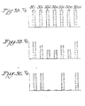
- Figures 3A-3C illustrate the operations as applied to the memory cells 30 and more particularly as reflected in the voltages across the elements 31 of the cells 30.
- Fig. 3A illustrates the voltages on cells 30 i to 30 vii which are set at +5 by the above-described clear operation which sets all the diodes high.
- Fig. 3B shows the cell 30 i-vii in various degrees of discharge after exposure to the light image from the optical system 10.
- Fig. 3C shows the evaluation of the cells upon conversion to the conform to the binary code of "l"s and "0"s in relation to the threshold voltage of +2.5V.
- Fig. 4A is agraphic illustration on a CRT screen of representative memory cells of RAM 16. The absence of shading represents the points of the array of the RAM 16 whose relative position represent values on the X- and Y-axes which are critically relatable to a viewed object.
- Fig. 4B is a graphic illustration of the image produced on the cells by the incident light from the system 10 when an object 15 is sensed and its image frozen in the cells 30. These cells 30 upon which light falls, are discharged, shown in Figs. 3A-3C lacking voltage above the threshold voltage and therefore represented by a logic 0 and in this embodiment by an absence of shading. Contrariwise, the cells upon which no light falls remaining above the threshold are represented by a logic 1 and the presence of shading.
- the illustration has only two shades, white and black representing logic 0 or logic 1, respectively.
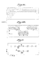
- Fig. 5 is a graphic illustration of values on the X-and Y-axis of representative memory cells at a few of the critical points determined in establishing the characteristic features of the sensed object, such as dimensions. These representative points are determined in this described preferred embodiment of the invention by a skeletonization process.
- This skeletonization takes place in a learning mode in which an object 15 of Fig. 1, which is a standard accurate, predetermined dimension, is sensed in the optical system 10.
- the light beam 14 emitted from system 10 of Fig. 1 after sensing the standard object 15, produces an image on the cells 30 of RAM 16 of Fig. 1 which precisely defines the searched-for dimensions in charged and discharged cells 30 (Fig. 3) as shown by light and dark areas in Fig. 4B.
- the myriad cells 30 of the RAM 16 array comprising these light areas of Fig. 4B are resolved by skeletonization to key, critical points for the inspection procedure described in greater length below.
- the imaged cells which make up each of the unshaded areas of Fig. 4B constitute a set.
- the edge of the unshaded area is a boundary.
- a certain cell is within the set and within a circle the radius of which is the distance from the cell to the boundary.
- the cell is a skeletal point if there is no other circle with the same center X and a greater radius contained in the set, which touches at least two of the boundaries.
- the union of all skeletal points in the imaged cells is a skeleton or medial axis.
- An algorithm can be devised to define the skeletal pixels.
- the base structure of the standard object 15 is looked for by means of a thin algorithm applied to the RAM 16 by tansmission through bus 26 from a program in EPROM 23.
- This skeletonization identifies specific critical data points comprised of cells marking the center lines 27 of the involved sets as shown in Fig. 4B. Then from this sub-set the logic looks for the particular transition points. For example, from critical data points in the order of 256 points the 14 points illustrated in Fig. 5 can be located.
- the representative dimensions of height and width of the three dimension standard object are indicated by appropriate arrows and legend in Fig. 4B.
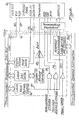
- Fig. 6 shows a general block diagram of the circuitry of the interface with the photosensitive RAM 16.
- the RAM 16 is a dynamic RAM chip. As stated above in one embodiment it has a total of over 65 thousand imaging locations. Each location is a cell which is sensitive to light as explained above with reference to cell 30 illustrated by Fig. 2. Each of these elements in the matrix has a light-sensitive component. Each memory cell than can be accessed randomly by simply reading in the appropriate row and column address. Light striking a particular element causes the capacitor, which is initially precharged to a fixed voltage, to discharge toward 0 volts. The capacitor discharges at a rate proportional to the light intensity through the duration of the exposure.
- each cell is made up of an electronic unit that discharges with light by converting light levels into electrical current.
- the current which leaks from the cell up to a level to effect a switching is a linear function of the light intensity. Accordingly, by adjusting the calibration of the cell it is possible to predetermine the amount of light that will bring about the switching, i.e. a specified amount of light will cause the sufficient discharge of the memory cell.
- the operations for establishing the predetermined standard or threshold is provided from the EPROM 23.
- the threshold voltage is established at +2.5 volts in each cell.
- the technique for use in connections with establishing the threshold voltage there is described the technique for use in connections with establishing the threshold voltage.
- the system illustrated in Fig. 6 includes means for selecting cells in the array, writing is the term used for placing information into a memory cell with a particular row and column address. Read is the term used for retrieving information from a memory cell with a particular row and column address. After the memory cells to be addressed are prepared, the write signal writes into these cells. The read signal retrieves information from these addressed memory cells. In short, the write and read signals are delivered to and from addressed locations which are the charged uncharged memory cells.
- the system 17 including means for selecting cells in the array, means for writing data into predetermined cells and means for taking data out.
- the optic RAM 16 is on the right side of the figure. According to an embodiment, one-half of the photosensitive cells are used.
- the transition points 28A and 28B of Fig. 5 are established in the learning mode in relation to a standard which is sensed.
- the bus 22 accesses the preselected cells, together with appropriate RAS, CAS, R/W lines 33, 34 and 35 provide the random access and column access strobes and read/write signals respectively.
- the RAS performs a further function in conjunction with the refresh operation.
- Refreshing the image sensor is a process used in a dynamic memory: the existing charge in each cell is sensed, the voltage compared with a threshold potential, and a fresh potential of OV (for a logic 0) or +5 V (for 1) is rewritten into the cell. If the image sensor is not continually refreshed, the light focused on each cell causes the voltage of the light. When the image sensor is not being refreshed, it is light sensitive. Refreshing is accomplished by sequencing through all 256 rows every 1/8 millisecond. This action restores the charge. This refresh action is controlled by latch 36 provided by line 37. In. this embodiment the threshold is 0.
- a DATA IN line 38 transfers data into the photosensitive RAM 16.
- a DATA OUT line 39 transmits.
- the memory cell at each image location of the RAM 16, being sensitive to light, is effected by the photodiode current which in turn means that light renders the diode conducting.
- the light intensity in turn determines cell discharge current and establishes the memory cell voltage level.
- the data transferred by line 38 and 39 in and out of the RAM 16 is in the form of binary information or code. Each transfer is in the form of a 1 or a zero. Data read from the cell is either a 1 or a zero.
- a preset threshold value determines the voltage level of the cell at which the photodiode switches the cell from the transferring a 1 to transferring a zero, or vice versa. The threshold is set on signals through line 40.
- the threshold value is calculated and held constant. For each cell the output data is related to whether the cell voltage is above or below the threshold.
- the output is a 1. If the cell voltage is less than the threshold, the output is a zero. Whether the cell voltage is less than or greater than the threshold is effected by the light directed at the semiconductor junction and the resulting current.
- a power line 41 supplies a +5 volt potential to RAM 16 and a ground 42 is indicated.
- the operation of the apparatus in the inspection process involves a number of steps centering around the digital image sensing device, the RAM 16.
- the imaging of the objects by exposure of the photosensitive RAM is a step in the process.
- a representative imaging in cells 30 has been described and illustrated above with respect to Figs. 2 and 3.
- Thus data is provided in cells 30 of RAM 16.
- the first step is to clear the cells of the RAM 16 to logic ls.
- the standard object is sensed in the optic system 10 and the image of the object is exposed on the RAM 16.
- the data in the cells produced by the light is read out.
- the charge on the cells defining the image is adjusted to provide charged cells of logic ls and discharged cells of logic Os to mark the center line of the base line cells, which circumscribing the image as established in charged and discharged cells, confine the important cells to a substantially reduced number, and to mark the important cells.
- the background or interior points are ignored as not important.
- This skeletonization to the baseline image cuts down the number of data points from which critical data points are selected to delineate the reference image. For example, thinning may produce 256 baseline points and 32 specific points selected which'forming a reference line characterize the inspected object and should be present on every qualified object. Transition points are sought and detected on the sample image. The height and length values are represented by the transition points illustrated and described in connection with Fig. 5
- the memory cells are inspected by addressing in sequence by transmitting address information on the address bus.
- the program from EPROM 23 searches for the cell with data, in this case zeros, and directs that a table of addresses be established in the storage RAM. If the transmission is to be an established address in the table, the inspection proceeds to the next point on the RAM 16. If the designated and establihsed point is not identified, the program branches to an alternate point or searches for it.
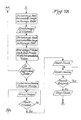
- Figs. 7A-7C show a computer program flow diagram for the system illustrated in the figures and described herein.
- the terminal steps are indicated with a bubble
- the input/output steps indicated with parallelograms
- the processing steps are indicated with rectangles whereas the decision or logic steps or questions are shown within diamond-shaped spaces.
- the system is turned on.
- the system is subject to a test for failed components.
- This test is comprised of a write and reading sequence of many addresses.
- This write/read sequence is equivalent to a RAM memory test.
- all the memory pixels to be used:inthe optic RAM are checked by this write/read sequence.
- This test serves to establish the presence of all detectors. The number of detectors being used in the system is determined by the program of the EPROM.
- the program in the display sequencing mode performs imaging by transferring data from the optic RAM to display memory. Each detector image is displayed for approximately a second.
- the display mode produces on the TV monitor briefly the image scene generated on the optic RAM by the optical system.
- This imaging feature is employed, for example, to provide adjustment of the image focus and illumination intensity.
- the display mode will proceed through all the detector images including those units of multiple optic RAMS and the system remains in this mode, sequencing through all the detector images until the program is switched to the LEARN mode.
- the LEARN mode is a routine made up of instructions to determine for the apparatus the features of a proper standard product for the purpose of making a comparison of a number of manufactured products with the proper standard product.
- the EPROM program looks for the characteristic image on the optic RAM of an object in the optical system.
- a standard object of proper dimensions is positioned in the optical system.
- the image of this proper standard object is then grabbed by exposure of the light image to the detectors of the optic RAM.
- This image is then retained or frozen on the optic RAM by the refresh signal which the computer produces for the optic RAM.
- the image then reamins frozen as long as the refresh signals continue or unitl the LEARN mode is completed.
- the image of a proper object is grabbed retained on the optic RAM and skeletonized by the thinning steps.
- the skeletonization of the image reduces the broad lines to the single pixel line image characteristic of the product as described in reference to and illustrated by Figure 5.
- the thinning may be accomplished in a standard manner, including those described in Algorithm for Graphics and Image Processing by Theo Pavlidis, Computer Science Press (1983), see pages 195 et seq.
- the thinning includes a way of simplifying pictorial forms.
- the following refers to skeletonization.
- the binary image is sharpened by a thinning technique.
- a program in the EPROM reduces the region defining the edges of the objects to a minimal cross-sectional width of a single line representing the cells of the optic RAM.
- the operation of the thinning algorithm is indicated by explanation set forth below.
- the thinning algorithm which can bedevised to provide the thinned image line for the operation in the present system looks for the base structure needed. It marks the center of these images and identifies the specific critical data points. Then from these the programmedprocedures look for the transition points.
- FIG. 5 shows a representation of thinnedline 27 of Fig. 4B as stored in the memory of computers by the procedures des- ribed above. The positions of the stored data are indicated in the storage memory of RAM 19 of Fig. 1.
- the transition point A is identified on thinned line 28A. Imediatley below his thinned line 28 a skeletonized line image of a newly iewed object is illustrated by thinned line 28B.
- the thinned Jine 27 of Fig. 4B is thus shown in Fig. 5.
- Figures 4A, 4B and 5 illustrate the operation of this algorithm applied to the object under examination.
- the thin line provides a definition of the points of the imaged object. It thus shows that given the image object we can construct the skeleton points, each of which has an associate X- and Y-value.
- the skeleton is obtained from the optic RAM array data.
- the skeletons consists of the points of the array whose relative position show values on the X- and Y- axes which are related to the viewed object.
- the learn routine then directs that the address information from the data of the critical points is stored into different locations in the storage RAM which have been cleared by the EPROM program for the information to be written in and stored at these locations. Then further successive images are grabbed, frozen, and skeletonzied.
- the learn routine in the EPROM then evaluates the information from the data of the critical points to make the determination of whether the thinned image is a reference line or a product. To be a reference line the line should not exceed the limits of an unthinned line. These are illustrated in Fig. 4A, that is the maximum and minimum line are represented in Fig. 4A.
- the grabbing of images and the number of images processed from the optic RAM for providing data of the ciritcal points is a random process for attaining a good statistical result.
- the skeleton of the firm image which is stored in the storage memory is of a proper object.
- Point A of Fig. 5 is of prime significance.
- the skeletonizing of the first image reduces the broad lines to the single pixel line image characteristic of the product. This is illustrated in Fig. 5. Registration is referenced to the first transition point in the skeletonized line. This is Point A.
- the program checks to determine if the image is of the product, or reference line. If not a reference, then a product, the program proceeds to find the first transition Point A. Registration of the image is carried out with respect ot this Point A, or first edge.
- Registration that is establishing the registration point, occurs before accumulation of the image. Registration assumes that a previous skeletonized line image, exists in the storage RAM. This has taken place with a proper object being viewed. With the proper object, after skeletonization, the line data is stored in the storage RAM by a storing step which consists of scanning the locations of the storage RAM and reading out of the optic RAM the digital data of the memory cells carrying the line data. The Y coordinate values of the thinned line are written into the memory locations in the storage RAM.
- the purpose is to reach a minimum variation of the standard deviation of the data. At this point sufficient data has been taken and the edges of the product images are determined.
- succeeding objects are sensed and exposed on RAM 16 and the image grabbed and retained on the RAM 16.
- the image is skeletonized to a base line image.
- the X- and Y- coordinates of the skeleton are accumulated in the storage RAM.
- This accumulation in the register of the storage RAM 19 of the succeeding objects provides the information for determining the product edges for the subsequent operation.
- This is achieved by an averaging step in which the Y values of two images of thinned lines are averaged by simple addition and division of the Y values by the program in the EPROM 23. And the averaging of successive Y values is carried cut by looping a given number of times, for example five times.
- the EPROM 23 program performs the averaging by looping with this data. Then the EPROM 23 puts into the storage RAM 19 the averaged points of the Y values on the points on the X-axis. Thus there is saved in the memory of the storage RAM 19 a table of standard Y values along the X-axis.
- This routine is followed to provide the vital pixels for the width, height and length of the examined product.
- the routine determines the length by an elapsed time method.
- the length may also be measured if optical detection system 10 is rotated 90° so that the detector is perpendicular to the motion of the product.
- the optic RAM 16 is reset by writing ls and then the system is exposed. Objects then moving past in the optical system 10 cause the base line image to disappear when an object reaches the base line in the image projected by the system.
- the clock values determined by a timer of its appearance and disappearance from the optical system become a means of measurement which being stored is accumulated for a number of successive objects.
- width and height two values are by simple addition and division by the EPROM 23 program. And the averaging of successive clock values is carried out by looping a given number of times. By continually taking samples, there are addition to the data to make another determination. Finally, a condition is reached when the standard deviation does not change significantly, then sufficient standard samples have been measured and sufficient data acquired. When the decision is reachedthat sufficient data on length has been gathered the looping is terminated and the learn mode is terminated.
- the RUN mode is started and the pixel points determine by the above procedure as key points are monitored. Not only the first transition point (A) but all the points on the table are checked. On the CRT these points will show the clear line when the detector is exposed to the image light. On checking for the reference line if it is present the steps of clearing and exposing is repeated and looped until the loose reference line disappears indicating a product has entered the imaging field.
- the predetermined sample pixels are checked for the object edges.
- the image offset values - the X and Y pixel shift necessary to register the RAM image left edge with the corresponding edge of the standard is calculated.
- the image values are compared with the standard value. The difference between the two values determines the magnitude of the error.
- the EPROM 23 program obtains a location on the X- and Y- axis from the storage RAM 19 and sends a signal to the RAM 16 at that location. If it is present it moves on to the next reference point. If it is not present, it searches within a fixed arm, determined by a predetermined pattern, from example a 5 pixels dimension pattern. If it finds a location the offset value is saved and stored to remember the difference. If no location is found the sensed object is rejected. The process is repeated by branching to the point before.
- the first test checks for low error value and the second test checks for high error value. Each results indicate whether the product is beyond acceptable limits.
- This invention can be used on a 6502 microprocessor, which is in Apple computers and Commodore computers.
Landscapes
- Engineering & Computer Science (AREA)
- Physics & Mathematics (AREA)
- General Physics & Mathematics (AREA)
- Quality & Reliability (AREA)
- Computer Vision & Pattern Recognition (AREA)
- Theoretical Computer Science (AREA)
- Length Measuring Devices By Optical Means (AREA)
- Image Analysis (AREA)
Abstract
A computer operates on manufacturing apparatus to measure articles (15) processed in the apparatus and to approve and select or reject the reviewed and measured articles (15) in accordance with parameters established by an optical system. This optical system on sensing an inspected article (15) forms an image on a photosensitive random access memory (16) and information relating to the image is sorted in an electronic system (17). The image information which is transmitted in bits, includes dimensional values, such as height, width and length, and the operation selects and approves articles (15) which are being detected as being within a predetermined average deviation in these dimensions. The information on the predetermined average deviation of dimensions is established by checking a representative number of articles (15). In the selection process bits from the sensing of the inspected article (15) are read from the photosensitive memory (16) and compared with stored data. If a significant difference is detected the inspected article (15) is rejected.
Description
- This invention relates to a method and apparatus for checking articles against a standard.
- Many methods and apparatus are known for checking articles for conformity of a parameter or parameters thereof, for example their dimensions, with a standard parameter value.
- In known methods and apparatus an article to be checked is illuminated with a light beam from a source such as a laser or an incandescent or strobe lamp, and the light reflected from the article detected on a photodetector such as a television-type detector device, a vidicon, an array of photosensitive elements or a photomultiplier tube.
- The detected light from the article provides information about parameters of the article, which can be compared with standard values in order to determine conformity of the article with a standard.
- In US-A-4111557 there is disclosed a method for optical determination and comparison of shapes, in which a line or point of light is projected onto an article by a source. The reflected rays are received by a TV camera or a photodiode matrix. The image signals are converted to digital data which is passed to a computer unit having storage. The stored values are compared with standard values to determine their difference from the standard. The resulting data is output from the computer to a plotter and/or a monitor.
- US-A-441456 discloses a sorting and inpspection apparatus which digitizes a TV camera output. The digitized output is stored and compared with a previously stored image which was recorded by placing a standard article in front of the TV camera.
- US-A-4343553 discloses a split or line projector with two image detectors positioned at 45° for testing the shape and height of a soldered joint. The resulting video signal is compared with first and second references to determine whether the joint is over soldered, under soldered, or acceptable.
- US-A-4105925 discloses an optical article locator with a left and a right light source each emitting light in a sheet at an acute angle to a conveyor belt surface. A linear diode array is positioned above the conveyor belt between the two light sources and is narrowly focused on a line of light formed at the intersection of the two sheets of light. The output from the linear diode array is provided to a programmed computer or microprocessor in a control unit for determining the position and orientation of articles on the conveyor belt passing through the field of view.
- US-A-3,667,846 discloses an optical surface inpection apparatus for detecting microscopic variations in a surface area and producing signals which are compared with the signals of a predetermined reference surface. A light source projects a spot of light onto the surface from an angle and the reflected light is sensed by an optical detector also set at an angle to the surface.
- US-A-3,796,492 discloses a laser dimension comparator in which two beams of light are set at an angle to the surface being evaluated and reflected to a vidicon whose output signals are processed and digitized. The measured dimension is then displayed on a digital display. In its initial operation, a reference surface is positioned at a fixed distance from a gauging head on the vidicon to obtain a reference surface which is stored in a comparator circuit for subsequent comparison to actual work pieces.
- US-A-3,791,741 discloses a size gauging and quality-inspecting apparatus in which articles are inspected in two successive inspection stations. The items are illuminated and the reflected light is detected by an optical sensor. The modulated light is electronically measured to produce signals corresponding to dimensions which are compared to a predetermined standard.
- US-A-4,311,392 discloses a thickness measuring apparatus with a light projector and an optical detector set at 45° to the surface of a sheet being evaluated. A processing mechanism calculates the thickness of the sheet based on the relative surface positions of the sheet and a metal roll over which the sheet is moved.
- US-A-4,139,304 discloses measuring variations in distance to a surface and determining surface contours using spaced-apart projected sheets of light which intersect the surface and a photodetector which receives the reflected light at an angle.
- US-A-4,146,926 discloses a method and apparatus for optically exploring the surface of an article in which a laser beam is scanned over the surface. Reflected light beams are received by a TV camera. The output signals from the TV camera are used by a computer to determine the contour and height dimension of a point on the surface of the article.
- US-A-4,279,513 discloses an optical, electronic measurement system which scans and images only the edges of a work piece. The measurement system is initially calibrated by positioning a work piece of known dimensions in the field of view; storing the signals representative of the standard of known work piece; and comparing similar work pieces of unknown dimensions to the standard.
- According to this invention there is provided a method of checking an article for conformity thereof with a standard, in which the article is illuminated with incident light and light reflected from the article is detected with a detector device which converts the detected light into electrical signals which are compared with signals representative of a standard article using a computer, characterised in that the detector device is a photosensitive random access memory device which is read directly by the computer to obtain said electrical signals.
- Preferably the method is characterised by the steps of moving a succession of articles; projecting incident light in at least one single line to the succession of articles and applying the line of light successively to the moving articles to illuminate each article with said light; detecting with the photosensitive random access memory the incidence of said line of light at said articles; operating a system computer comparator in response to inputs representing the detected light to produce information about the dimensions of each article in the photosensitive random access memory; retaining and storing said information in a separate random access memory; storing information of a standard value of the dimensions of each article in said separate random access memory; determining the information of each article on said photosensitive random access memory; transferring the data directly to the separate random access memory in digital form; and comparing the information on the standard image and each article.
- Also according to this invention there is provided a method of checking articles for conformity of a parameter thereof with a standard parameter value, the parameter being measured optically and compared with the standard parameter value using a computer, characterised in that the standard parameter is derived from a plurality of parameter measurements carried out on a plurality of articles
- Further according to this invention there is provided apparatus for inspecting by illumination a succession of articles to detect physical characteristics as compared to a standard and making a determination of conformance with the standard, characterized by dimension-detecting apparatus providing digital signals obtained by scanning an image optically produced on a photosensitive random access memory from an article and.detecting an abnormal state of the dimension of said article so as to classify the article, said dimension detecting apparatus comprising means sensing and measuring a series of standard articles; means for producing a model means characteristic of an article with dimensions within the range of a predetermined deviation; and means for scanning the image output, of sensing and measuring each image optically produced from an article and for detecting the dimensions of each article so as to classify each article.
- Devices of the type of an all-digital image sensing device are disclosed in the article entitled "A 65K-bit dynamic RAM chip is the visual sensor in this digital image camera" by Steve Ciarcia, BYTE, September, 1983, Vol. 8, No. 9, page 21 and October, 1983, Vol. 8, No. 10, page 67. Also reference may be had to US-A-4,441,125, particularly Fig. 2.
- The system of writing computer instructions and statements for a program has as its ultimate objective an application of the program which results in the selection and approval of articles within the range of the determined average deviation. Also defective articles are identified and the nature of the defects noted and collated.
- Stated briefly, specific bits from the sensing of an inspected article are read from the cells of the storage photosensitive memory and compared with the stored product data contained in the storage memory. While this comparison is taking place, the optical system is sensing a succeeding article.
- If the comparison discovers a significant difference between an inspected article and the standard, the inspected article is selected for rejection, and the amount of deviation may be noted and used for trend analysis.
- The optical system involves a beam of light in a single line or grid pattern directed at and incident on the articles which may be moving on a conveyor system and transversely across the articles. Preferable the beam of light is directed at the plane at an angle of 45°. It is an advantage that the setting of the angle of 45° causes the object to create a break in the line of light into two separate lines. The distance of the separation between these lines is equal to the height of the bar. This break in the lines is detected and transferred to the photosensitive memory. A dynamic memory integrated circuit chip is used as memory for a microprocessor and by permitting light to strike the die when the refresh is off, the same device becomes a photosensitive detector array for optical images. The use of this technique eliminates the need for a television camera, or working with a whole image or an analog to digital converter or the computer image processing time required to produce a binary image suitable for standard measuring algorithms.
- Of advantage is projecting light in at least one single line, detecting a break or separation in the line into two lines and making a comparison with the separation in the image of the standard and the successive images of the moving articles on the conveyor system.
- The image that is produced on the photosensitive memory by the standard is comprised of a large number of memory cells of the memory. In a thinning procedure specific critical cells are identified as representing the body of the article. Further of these specifically identified cells, there are cells which are identified as located with transition points (edges) in the image of the article.
- These cells at the transition points in the present embodiment contain data in the form of bits, a loss, or lack of charge or a logic "0". This information through the action of the program in the processing units is transmitted in bit form to the storage memory where it is stored as an address table.
- When the inspected articles are subsequently sensed and imaged on the photosensitive memory, the specific cells at the transition points are discharged. This logic 0 on these few vital cells is detected and digitally read out to the storage memory for comparison.
- A significant aspect in the imaging, detection and transmission procedure involving the photosensitive dynamic memory lies in the speed provided which in turn has a faster refresh signal to maintain the image. This refresh signal proceeding every 1/8 millisecond through the memory keeps the data available for read out. Because of this high speed the refreshing preserves uniform exposure of the images on the memory.
- Another significant advantage of the processing of the values by digits is the tolerances that can be provided for. For example, to compensate when the correct transition points cannot be located in the imaged cells, the program signals locate and detect the cell having the data. This data is then read out of the photosensitive memory to the storage memory where the correct points are stored.
- This invention will now be described by way of example with reference to the drawings, in which:-
- Fig. 1 is a diagrammatic view of essential parts of apparatus incorporating a photosensitive random access memory according to the invention;
- Fig. 2 is a circuit diagram representative of a memory cell of the photosensitive memory;
- Figs. 3A-3C present bar charts of images on the photosensitive memory.
- Figs. 4A and 4B are graphic illustrations on a CRT screen; Fig 4A without a sensed article and Fig. 4B with a sensed article reproduced on the photosensitive memory;
- Fig. 5 is a graphic illustration on the X- and Y- axes of the photosensitive memory of representative memory cells in the imaging of a second article;
- Fig. 6 is a block diagram illustrating the organization associated with the photosensitive memory and the electronic system apparatus of the invention; and
- Figs. 7A, 7B and 7C are flow charts for the method of operation according to the invention.
- Fig. 1 shows an embodiment of a measuring apparatus for bodies. An
optical system 10 is comprised of anobject lens 13, and a source of light 11, and a condenser lens 12 which project alight beam 14 in a pattern at and incident on anobject 15. Particularly theobject 15 may be in motion on a conveyor system not shown and the light beam is directed and incident on the object transversely accross the object. The beam oflight 14 is directed at a plane of the object at an angle of 45° and the setting of the angle of 45° causes the object to create a break of the line of the light beam into two separate lines. This distance of the separation of these lines is proportional to the height of the object. - The light beam and the break in the line is transferred and directed to a
photosensitive RAM 16. - The
RAM 16 is an integrated circuit that linearly converts light level into electrical current. It is designed as an imaging device made of memory cells. In one preferred embodiment the memory cells are arranged in a regular pattern of 256 elements in a row by 128 elements in a column. This embodiment provides 32,768 discrete imaging locations. - The
RAM 16 is a memory in conjunction with asystem 17. TheRAM 16 acts as a detection mechanism to be described further below. - In the embodiment of the invention illustrated by and described in relation to Fig. 1, the
system 17 includes a CPU (central processing unit) 18, aRAM 19, which are interconnected and connected to theoptic RAM 16 by adata bus 20. TheCPU 18 is connected also by a control bus 21 and anaddress bus 22. An EPROM unit 23 is connected by thedata bus 20 and theaddress bus 22. The EPROM interconnects with theCPU 18 by bus 24 and withstorage RAM 19 bybus 25. - The image analysis with the necessary computer operations is processed in the electronic hardware of
system 17. The image of theobject 15 as viewed by thesystem 10 is retained on the photosensitivedynamic RAM 16 and is involved in the processing which is described further hereinafter. In a preferred embodiment, each of a succession ofobjects 15 are removed and replaced successively in theoptical system 10. A feature of an inspection procedure according to this invention is that checking the inspected objects in practice involves reading only critical points of the retained image onphotosensitive RAM 16. It is the critical dimensions of the inspected objects 15 that are detected and stored in the memory ofRAM 19. Then these detected and stored dimensions are compared with standard dimensions of theobject 15 stored inRAM 19. In this way deviations that may occur in the successive inspectedobjects 15 are detected. The EPROM 23 provides the programming of the initial analysis and the detection comparison, decisions and subsequent action. - The
photosensitive RAM 16 is a memory related to thesystem 17 and acts as a detection mechanism. - The memory cells in the array can be randomly accessed. This is done by row and column address strobes. As explained below, the row address strobe first addresses a row in which a cell to be accessed is present and then the column address strobe addresses the column of the particular memory cell. The confluence of these row and address strobe makes the data available on the particular cell.
- Fig. 2 is an illustrative circuit diagram of a
memory cell 30 of theRAM 16. Thecell 30 contains aphotosenstive element 31 illustrated in Fig. 2 as an n-channel unijunction transistor. Thememory cell 30 is a single transistor dynamic cell. Theelement 31 controls access to thestorage capacitor 29. The capacitance ofcapacitor 29 exists between the drain of theelement 31 and ground. The other contact to the drain is connected to a column of theRAM 16 array and the gate is connected to a row - Each
memory cell 30 is precharged to a fixed voltage of +5 volts. These individual cells after this charging to 5 volts are discharged by light incident on thephotosensitive element 31. In FiG 2, the incident light is represented by the broken arrow falling on theelement 31. Thecapacitor 29 charged to +5 volts is discharged as theelement 31 photosensitivity cause a flow of current through the channel. The discharge from the +5 volts depends upon the intensity of the light during the exposure of the element to the light. As the discharge continues as long as the light falls on theelement 31, the capacitor voltage can be reduced to a value below the threshold setting of the comparator. - When the capacitor voltage value has been discharged below a fixed threshold voltage, the cell will be read as not containing a
logic 1 but as having a logic 0. - To read the information on memory cells 30 (Fig. 2) the column line is connected to the voltage source and then released and the row line is raised as by signal. If the capacitor 29 (Fig. 2) is at a low voltage, the result is a lowering of the voltage on the column line. This lowering of the voltage on the column line is detected by a sensing amplifier driver and the data output line is driven to 0. This is illustrated in Fig. 2.
- In a particular advantage, if the memory cells are to take a new image the cells are cleared by restoring full charge to them. Clearing or charging a row at a time of the memory cells is accompalished by reducing the threshold voltage to 0 volts and refreshing. During comparison in the reference cycle the charge on the cell capacitor can never be zero when sensed, but the threshold has been set at zero volts. Therefore, the charge on the cell capacitor must be greater than the reference value. This forces the memory cell to be refreshed to the high state resulting in clearing the cell. When the refrence value is zero, it is impossible for the cell to have 0 charge. Therefore, it is forced back to full charge. The refresh cycle is accomplished with hardware, operating near the component speed limitations (optic RAM access time). This is accomplished in 128 microseconds (.000128 seconds).
- This method has two advantages. First, the normal refresh rate on the optic RAM is increased to 8 times per millisecond causing the instrument to do a better job of "freezing" the image on the optic RAM. Second, the optic RAM can be isolated from addresses generated by the processor for program execution. If it were not isolated, an effect occurs which is seen as rows or sections of the image less sensitive to light (appearing as black lines).
- Figures 3A-3C illustrate the operations as applied to the
memory cells 30 and more particularly as reflected in the voltages across theelements 31 of thecells 30. Fig. 3A illustrates the voltages on cells 30 i to 30 vii which are set at +5 by the above-described clear operation which sets all the diodes high. Fig. 3B shows the cell 30 i-vii in various degrees of discharge after exposure to the light image from theoptical system 10. Fig. 3C shows the evaluation of the cells upon conversion to the conform to the binary code of "l"s and "0"s in relation to the threshold voltage of +2.5V. - Fig. 4A is agraphic illustration on a CRT screen of representative memory cells of
RAM 16. The absence of shading represents the points of the array of theRAM 16 whose relative position represent values on the X- and Y-axes which are critically relatable to a viewed object. Fig. 4B is a graphic illustration of the image produced on the cells by the incident light from thesystem 10 when anobject 15 is sensed and its image frozen in thecells 30. Thesecells 30 upon which light falls, are discharged, shown in Figs. 3A-3C lacking voltage above the threshold voltage and therefore represented by a logic 0 and in this embodiment by an absence of shading. Contrariwise, the cells upon which no light falls remaining above the threshold are represented by alogic 1 and the presence of shading. The illustration has only two shades, white and black representing logic 0 orlogic 1, respectively. - Fig. 5 is a graphic illustration of values on the X-and Y-axis of representative memory cells at a few of the critical points determined in establishing the characteristic features of the sensed object, such as dimensions. These representative points are determined in this described preferred embodiment of the invention by a skeletonization process. This skeletonization takes place in a learning mode in which an
object 15 of Fig. 1, which is a standard accurate, predetermined dimension, is sensed in theoptical system 10. Thelight beam 14 emitted fromsystem 10 of Fig. 1 after sensing thestandard object 15, produces an image on thecells 30 ofRAM 16 of Fig. 1 which precisely defines the searched-for dimensions in charged and discharged cells 30 (Fig. 3) as shown by light and dark areas in Fig. 4B. Themyriad cells 30 of theRAM 16 array comprising these light areas of Fig. 4B are resolved by skeletonization to key, critical points for the inspection procedure described in greater length below. - By the thinning technique the binary image is sharpened. A digital logic replaces the logic 0's obtained by exposure. This thinning logic decides that a cell belongs to the thinned line when it is on the medial vertical axis of all exposed cells. The imaged cells which make up each of the unshaded areas of Fig. 4B constitute a set. The edge of the unshaded area is a boundary. A certain cell is within the set and within a circle the radius of which is the distance from the cell to the boundary. The cell is a skeletal point if there is no other circle with the same center X and a greater radius contained in the set, which touches at least two of the boundaries. The union of all skeletal points in the imaged cells is a skeleton or medial axis.
- The usual idea in skeletonization or thinning is to sequentially remove the edges of the line to be thinned from storage until all that remains is a single line of bits only one bit wide.
- An algorithm can be devised to define the skeletal pixels.
- The base structure of the
standard object 15 is looked for by means of a thin algorithm applied to theRAM 16 by tansmission throughbus 26 from a program in EPROM 23. This skeletonization identifies specific critical data points comprised of cells marking thecenter lines 27 of the involved sets as shown in Fig. 4B. Then from this sub-set the logic looks for the particular transition points. For example, from critical data points in the order of 256 points the 14 points illustrated in Fig. 5 can be located. The representative dimensions of height and width of the three dimension standard object are indicated by appropriate arrows and legend in Fig. 4B. - Fig. 6 shows a general block diagram of the circuitry of the interface with the
photosensitive RAM 16. TheRAM 16 is a dynamic RAM chip. As stated above in one embodiment it has a total of over 65 thousand imaging locations. Each location is a cell which is sensitive to light as explained above with reference tocell 30 illustrated by Fig. 2. Each of these elements in the matrix has a light-sensitive component. Each memory cell than can be accessed randomly by simply reading in the appropriate row and column address. Light striking a particular element causes the capacitor, which is initially precharged to a fixed voltage, to discharge toward 0 volts. The capacitor discharges at a rate proportional to the light intensity through the duration of the exposure. When the cell's content is read, a logic 0 remaining in the cell indicates a bright pixel-the capacitor was exposed to a light intensity sufficient to discharge the capacitor past the threshold point. Thus each cell is made up of an electronic unit that discharges with light by converting light levels into electrical current. The current which leaks from the cell up to a level to effect a switching is a linear function of the light intensity. Accordingly, by adjusting the calibration of the cell it is possible to predetermine the amount of light that will bring about the switching, i.e. a specified amount of light will cause the sufficient discharge of the memory cell. The operations for establishing the predetermined standard or threshold is provided from the EPROM 23. - In one embodiment the threshold voltage is established at +2.5 volts in each cell. In the Encylopedia of Computer and Engineering, p. 953, for example, there is described the technique for use in connections with establishing the threshold voltage.
- Basically, the system illustrated in Fig. 6 includes means for selecting cells in the array, writing is the term used for placing information into a memory cell with a particular row and column address. Read is the term used for retrieving information from a memory cell with a particular row and column address. After the memory cells to be addressed are prepared, the write signal writes into these cells. The read signal retrieves information from these addressed memory cells. In short, the write and read signals are delivered to and from addressed locations which are the charged uncharged memory cells. Basically, the
system 17 including means for selecting cells in the array, means for writing data into predetermined cells and means for taking data out. - In Fig. 6, the
optic RAM 16 is on the right side of the figure. According to an embodiment, one-half of the photosensitive cells are used. Thetransition points 28A and 28B of Fig. 5 are established in the learning mode in relation to a standard which is sensed. - Reference is made to the legends which identify what occurs in this procedure.
- The
bus 22 accesses the preselected cells, together with appropriate RAS, CAS, R/W lines - The RAS performs a further function in conjunction with the refresh operation. Refreshing the image sensor is a process used in a dynamic memory: the existing charge in each cell is sensed, the voltage compared with a threshold potential, and a fresh potential of OV (for a logic 0) or +5 V (for 1) is rewritten into the cell. If the image sensor is not continually refreshed, the light focused on each cell causes the voltage of the light. When the image sensor is not being refreshed, it is light sensitive. Refreshing is accomplished by sequencing through all 256 rows every 1/8 millisecond. This action restores the charge. This refresh action is controlled by
latch 36 provided byline 37. In. this embodiment the threshold is 0. - A DATA IN
line 38 transfers data into thephotosensitive RAM 16. A DATA OUT line 39 transmits. - The memory cell at each image location of the
RAM 16, being sensitive to light, is effected by the photodiode current which in turn means that light renders the diode conducting. The light intensity in turn determines cell discharge current and establishes the memory cell voltage level. - The data transferred by
line 38 and 39 in and out of theRAM 16 is in the form of binary information or code. Each transfer is in the form of a 1 or a zero. Data read from the cell is either a 1 or a zero. In a useful operation of the apparatus a preset threshold value determines the voltage level of the cell at which the photodiode switches the cell from the transferring a 1 to transferring a zero, or vice versa. The threshold is set on signals throughline 40. - Under typical operating conditions the threshold value is calculated and held constant. For each cell the output data is related to whether the cell voltage is above or below the threshold.
- If the memory cell voltage is above the threshold voltage, the output is a 1. If the cell voltage is less than the threshold, the output is a zero. Whether the cell voltage is less than or greater than the threshold is effected by the light directed at the semiconductor junction and the resulting current.
- Further in Fig. 6, a power line 41 supplies a +5 volt potential to RAM 16 and a
ground 42 is indicated. - In general the operation of the apparatus in the inspection process involves a number of steps centering around the digital image sensing device, the
RAM 16. As the purpose of this process is to sense, evaluate and analyze a series of objects, the imaging of the objects by exposure of the photosensitive RAM is a step in the process. A representative imaging incells 30 has been described and illustrated above with respect to Figs. 2 and 3. Thus data is provided incells 30 ofRAM 16. - The first step is to clear the cells of the
RAM 16 to logic ls. Next the standard object is sensed in theoptic system 10 and the image of the object is exposed on theRAM 16. The data in the cells produced by the light is read out. Using the thinning algorithm the charge on the cells defining the image is adjusted to provide charged cells of logic ls and discharged cells of logic Os to mark the center line of the base line cells, which circumscribing the image as established in charged and discharged cells, confine the important cells to a substantially reduced number, and to mark the important cells. Thus only the cells at the critical points of the line image or objects edge involved in the procedure. The background or interior points are ignored as not important. This skeletonization to the baseline image cuts down the number of data points from which critical data points are selected to delineate the reference image. For example, thinning may produce 256 baseline points and 32 specific points selected which'forming a reference line characterize the inspected object and should be present on every qualified object. Transition points are sought and detected on the sample image. The height and length values are represented by the transition points illustrated and described in connection with Fig. 5 - The memory cells are inspected by addressing in sequence by transmitting address information on the address bus.
- The program from EPROM 23 searches for the cell with data, in this case zeros, and directs that a table of addresses be established in the storage RAM. If the transmission is to be an established address in the table, the inspection proceeds to the next point on the
RAM 16. If the designated and establihsed point is not identified, the program branches to an alternate point or searches for it. - Figs. 7A-7C show a computer program flow diagram for the system illustrated in the figures and described herein. In Figs. 7A-7C the terminal steps are indicated with a bubble, the input/output steps indicated with parallelograms, the processing steps are indicated with rectangles whereas the decision or logic steps or questions are shown within diamond-shaped spaces.
- The system is turned on. The system is subject to a test for failed components. This test is comprised of a write and reading sequence of many addresses. This write/read sequence is equivalent to a RAM memory test. In a second test all the memory pixels to be used:inthe optic RAM are checked by this write/read sequence. This test serves to establish the presence of all detectors. The number of detectors being used in the system is determined by the program of the EPROM.
- Next, the program in the display sequencing mode, performs imaging by transferring data from the optic RAM to display memory. Each detector image is displayed for approximately a second. Thus the display mode produces on the TV monitor briefly the image scene generated on the optic RAM by the optical system. This imaging feature is employed, for example, to provide adjustment of the image focus and illumination intensity.
- The display mode will proceed through all the detector images including those units of multiple optic RAMS and the system remains in this mode, sequencing through all the detector images until the program is switched to the LEARN mode.
- While the learn signal has not been produced, the program will continue the display sequence successively producing the detector images.
- When a learn signal is produced as by a positive actuation of the mechanical switch, the program branches to the LEARN mode.
- The LEARN mode is a routine made up of instructions to determine for the apparatus the features of a proper standard product for the purpose of making a comparison of a number of manufactured products with the proper standard product.
- If the program is switched to the LEARN mode, the EPROM program looks for the characteristic image on the optic RAM of an object in the optical system. A standard object of proper dimensions is positioned in the optical system. The image of this proper standard object is then grabbed by exposure of the light image to the detectors of the optic RAM. This image is then retained or frozen on the optic RAM by the refresh signal which the computer produces for the optic RAM. The image then reamins frozen as long as the refresh signals continue or unitl the LEARN mode is completed.
- In the LEARN mode, the image of a proper object is grabbed retained on the optic RAM and skeletonized by the thinning steps. The skeletonization of the image reduces the broad lines to the single pixel line image characteristic of the product as described in reference to and illustrated by Figure 5.
- The thinning may be accomplished in a standard manner, including those described in Algorithm for Graphics and Image Processing by Theo Pavlidis, Computer Science Press (1983), see pages 195 et seq. The thinning includes a way of simplifying pictorial forms.
- The following refers to skeletonization. The binary image is sharpened by a thinning technique. A program in the EPROM reduces the region defining the edges of the objects to a minimal cross-sectional width of a single line representing the cells of the optic RAM. The operation of the thinning algorithm is indicated by explanation set forth below.
- The thinning algorithm which can bedevised to provide the thinned image line for the operation in the present system looks for the base structure needed. It marks the center of these images and identifies the specific critical data points. Then from these the programmedprocedures look for the transition points.
- A graphic illustration of the operation of this feature is presented in a reproduction of the graph of Figure 5. Figure 5 shows a representation of
thinnedline 27 of Fig. 4B as stored in the memory of computers by the procedures des- ribed above. The positions of the stored data are indicated in the storage memory ofRAM 19 of Fig. 1. The transition point A is identified on thinned line 28A. Imediatley below his thinned line 28 a skeletonized line image of a newly iewed object is illustrated by thinnedline 28B. The thinnedJine 27 of Fig. 4B is thus shown in Fig. 5. - Location of the bits are stored in the RAM in a relationship which is in keeping with the pixels of the thinned line of the
optic RAM 16. Accordingly the relative position on the X- and Y-axes of the optic RAM are maintained. - As a result, the line representation of the object clearly expresses the structure relationship of the object under inspection. Figures 4A, 4B and 5 illustrate the operation of this algorithm applied to the object under examination.
- After skeletonization the thin line provides a definition of the points of the imaged object. It thus shows that given the image object we can construct the skeleton points, each of which has an associate X- and Y-value. The skeleton is obtained from the optic RAM array data. The skeletons consists of the points of the array whose relative position show values on the X- and Y- axes which are related to the viewed object.
- Then this image is stored in the storage RAM. The learn routine then directs that the address information from the data of the critical points is stored into different locations in the storage RAM which have been cleared by the EPROM program for the information to be written in and stored at these locations. Then further successive images are grabbed, frozen, and skeletonzied.
- While image is retained on the optic RAM the skeletonization identifies the critical points by the function of the thinning algorithm.
- The learn routine in the EPROM then evaluates the information from the data of the critical points to make the determination of whether the thinned image is a reference line or a product. To be a reference line the line should not exceed the limits of an unthinned line. These are illustrated in Fig. 4A, that is the maximum and minimum line are represented in Fig. 4A.
- The grabbing of images and the number of images processed from the optic RAM for providing data of the ciritcal points is a random process for attaining a good statistical result. The skeleton of the firm image which is stored in the storage memory is of a proper object.
- Point A of Fig. 5 is of prime significance. The skeletonizing of the first image reduces the broad lines to the single pixel line image characteristic of the product. This is illustrated in Fig. 5. Registration is referenced to the first transition point in the skeletonized line. This is Point A. When further images of successive and same objects are grabbed the program checks to determine if the image is of the product, or reference line. If not a reference, then a product, the program proceeds to find the first transition Point A. Registration of the image is carried out with respect ot this Point A, or first edge.
- Registration, that is establishing the registration point, occurs before accumulation of the image. Registration assumes that a previous skeletonized line image, exists in the storage RAM. This has taken place with a proper object being viewed. With the proper object, after skeletonization, the line data is stored in the storage RAM by a storing step which consists of scanning the locations of the storage RAM and reading out of the optic RAM the digital data of the memory cells carrying the line data. The Y coordinate values of the thinned line are written into the memory locations in the storage RAM.
- With succeeding objects by examination the first transition point of the image of a succeeding object in relation to the stored Point A of the standard proper object, there is a justification made between the position of the first transition point of the succeeding object as it appears in the storage RAM with respect to that of the proper object stored in the storage RAM. This justification takes place by determining the differences in the positioning on the X-axis and taking this difference into account in the subsequent operation.
- In the examination of succeeding objects as described above to accumulate data, the purpose is to reach a minimum variation of the standard deviation of the data. At this point sufficient data has been taken and the edges of the product images are determined.
- In this reaching a minimum variation, succeeding objects are sensed and exposed on
RAM 16 and the image grabbed and retained on theRAM 16. The image is skeletonized to a base line image. The X- and Y- coordinates of the skeleton are accumulated in the storage RAM. This accumulation in the register of thestorage RAM 19 of the succeeding objects provides the information for determining the product edges for the subsequent operation. This is achieved by an averaging step in which the Y values of two images of thinned lines are averaged by simple addition and division of the Y values by the program in the EPROM 23. And the averaging of successive Y values is carried cut by looping a given number of times, for example five times. That is the standard deviation for each point on the X- axis is calculated after sufficient data has been obtained, the EPROM 23 program performs the averaging by looping with this data. Then the EPROM 23 puts into thestorage RAM 19 the averaged points of the Y values on the points on the X-axis. Thus there is saved in the memory of the storage RAM 19 a table of standard Y values along the X-axis. - At the completion of this averaging and the resultant storage of a table of standard values the representative points provide the edges and thus the pixel addresses of the
RAM 16 which are to be sampled during the run of the system. - This routine is followed to provide the vital pixels for the width, height and length of the examined product.
- The routine determines the length by an elapsed time method. The length may also be measured if
optical detection system 10 is rotated 90° so that the detector is perpendicular to the motion of the product. Theoptic RAM 16 is reset by writing ls and then the system is exposed. Objects then moving past in theoptical system 10 cause the base line image to disappear when an object reaches the base line in the image projected by the system. Thus the object is sensed and the clock values determined by a timer of its appearance and disappearance from the optical system become a means of measurement which being stored is accumulated for a number of successive objects. - As with determination of width and height two values are by simple addition and division by the EPROM 23 program. And the averaging of successive clock values is carried out by looping a given number of times. By continually taking samples, there are addition to the data to make another determination. Finally, a condition is reached when the standard deviation does not change significantly, then sufficient standard samples have been measured and sufficient data acquired. When the decision is reachedthat sufficient data on length has been gathered the looping is terminated and the learn mode is terminated.
- The learning now being complete the NOT READY light is turned off and calculated object values can be displayed on the CRT for visualizing and recording in an appropriate log.
- The RUN mode is started and the pixel points determine by the above procedure as key points are monitored. Not only the first transition point (A) but all the points on the table are checked. On the CRT these points will show the clear line when the detector is exposed to the image light. On checking for the reference line if it is present the steps of clearing and exposing is repeated and looped until the loose reference line disappears indicating a product has entered the imaging field.
- As soon as the product appears, the time is noted on the clock register. This value is recorded and evaluated in relation to timing of a reappearance of the reference line.
- The predetermined sample pixels are checked for the object edges. The image offset values - the X and Y pixel shift necessary to register the RAM image left edge with the corresponding edge of the standard is calculated.
- The image values are compared with the standard value. The difference between the two values determines the magnitude of the error.
- In comparison of the image values the EPROM 23 program obtains a location on the X- and Y- axis from the
storage RAM 19 and sends a signal to theRAM 16 at that location. If it is present it moves on to the next reference point. If it is not present, it searches within a fixed arm, determined by a predetermined pattern, from example a 5 pixels dimension pattern. If it finds a location the offset value is saved and stored to remember the difference. If no location is found the sensed object is rejected. The process is repeated by branching to the point before. - Again when a product appears the sequence is repeated as described above. It is a feature of this invention that the error values are calculated. If the error is within the normal range the report so indicates, the product counter is incremented and the process is repeated.
- If the error calculation indicate a product outside the nominal error values other tests may he conducted to determine the extent of the error. The first test checks for low error value and the second test checks for high error value. Each results indicate whether the product is beyond acceptable limits.
- It can be seen that there has been provided a method and apparatus for establishing a standard of dimensions by sensing and establishinig parameters and more particularly by comparing and adjusting to a succession of standard objects to reach a minimum of standard deviation by taking sufficient data. And then using this calculated standard deviation in sensing and measuring a run of articles moving successively and continuously. The moving articles thus sensed and measured and compared are identified as normal or beyond the limits.
- The references, BYTE, September and October 1983, Vol. 8, Nos. 9 and 10, U.s. 4,441,125 and Algorithms for Graphics and Image Processing, Pavlidis, are relevant to the present disclosure.
- This invention can be used on a 6502 microprocessor, which is in Apple computers and Commodore computers.
Claims (8)
1. A method of checking an article (15) for conformity thereof with a standard, in which the article is illuminated with incident light (14) and light reflected from the article (15) is detected with a detector device (16) which converts the detected light into electrical signals which are compared with signals representative of a standard article using a computer, characterised in that the detector device (16) is a photosensitive random access memory device which is read directly by the computer to obtain said electrical signals.
2. A method as claimed in Claim 1, characterised by the steps of moving a succession of articles (15); projecting incident light (14) in at least one single line to the succession of articles (15) and applying the line of light (14) successively to the moving articles (15) to illuminate each article (15) with said light (14); detecting with the photosensitive random access memory (16) the incidence of said line of light (14) at said articles (15); operating a system computer comparator in response to inputs representing the detected light to produce information about the dimensions of each article (15) in the photosensitive random access memory (16); retaining and storing said information in a separate random access memory (19); storing information of a standard value of the dimensions of each article (15) in said separate random access memory (19); determining the information of each article (15) on said photosensitive random access memory (16); transferring the data directly to the separate random access memory (19) in digital form; and comparing the information on the standard image and each article (15).
3. A method according to Claim 2, characterised by viewing the articles (15) in an optical system successively forming images of each article; repetitively measuring the dimensions of the articles; creating and storing in a memory data of the dimensions of each article; providing a data processor with the data of the dimensions of the articles; repetitively comparing the dimensions of the articles to create an average of the dimensions; storing data of the average of the dimensions in said memory; monitoring conveyed articles by viewing said conveyed articles in said optical system; ascertaining on the basis of the monitoring of the conveyed articles whether the dimensions of said articles are in accordance with said average of the dimensions; and halting the conveyance of an article when the dimensions thereof have failed to correspond to the average of dimensions.
4. A method according to Claim 2, characterised in that the image on the photosensitive random access memory (16) is thinned to provide a skeletonized image of each article (15); bits from the skeletonized image are detected and stored located in the storage RAM (19); successive articles (15) are inspected and bits are detected and accumulated, the accumulated data being processed to establish a state and standard with a standard deviation; additional successive articles are inspected and imaged on the photosensitive random access memory (16); and the detected bits of the additional articles (15) are compared with the bits of the established standard to determine any difference.
5. A method according to any preceding claim, characterised in that individual cells of the photosensitive memory (16) are precharged to a fixed voltage; individual cells are selectively discharged by the reflected light to reduce the voltage, the selective discharge of the cells being read by determining the reduced voltage on the column line of the memory (16), the detecting of the reduced voltage being effected by a sensing amplifier.
6. A method according to Claim 5, characterised by the steps of reducing a threshold voltage on the cells of the photosensitive memory (16) to zero; detecting the voltages on the imaged cells; sensing the image of the imaged cells in the detected voltages in said cells; and refreshing the cells to a high state while the threshold voltage is at zero the refresh cycle taking place in the order of the photosensitive memory access time.
7. A method of checking articles (15) for conformity of a parameter thereof with a standard parameter value, the parameter being measured optically and compared with the standard parameter value using a computer, characterised in that the standard parameter is derived from a plurality of parameter measurements carried out on a plurality of articles (15).
8. Apparatus for inspecting by illumination a succession of articles (15) to detect physical characteristics as compared to a standard and making a determination of conformance with the standard, characterized by dimension-detecting apparatus providing digital signals obtained by scanning an image optically produced on a photosensitive random access memory (16) from an article (15) and detecting an abnormal state of the dimension of said article (15) so as to classify the article (15), said dimension detecting apparatus comprising means sensing and measuring a series of standard articles; means for producing a model means characteristic of an article with dimensions within the range of a predetermined deviation; and means for scanning the image output, of sensing and measuring each image optically produced from an article and for detecting the dimensions of each article so as to classify each article.
Applications Claiming Priority (2)
| Application Number | Priority Date | Filing Date | Title |
|---|---|---|---|
| US06/676,102 US4697245A (en) | 1984-11-29 | 1984-11-29 | Inspection and measuring apparatus and method |
| US676102 | 1991-03-27 |
Publications (1)
| Publication Number | Publication Date |
|---|---|
| EP0183565A1 true EP0183565A1 (en) | 1986-06-04 |
Family
ID=24713236
Family Applications (1)
| Application Number | Title | Priority Date | Filing Date |
|---|---|---|---|
| EP85308723A Withdrawn EP0183565A1 (en) | 1984-11-29 | 1985-11-29 | Method and apparatus for checking articles against a standard |
Country Status (2)
| Country | Link |
|---|---|
| US (1) | US4697245A (en) |
| EP (1) | EP0183565A1 (en) |
Cited By (1)
| Publication number | Priority date | Publication date | Assignee | Title |
|---|---|---|---|---|
| EP0355377A1 (en) * | 1988-08-05 | 1990-02-28 | Siemens Aktiengesellschaft | Method for testing optically flat electronic component assemblies |
Families Citing this family (19)
| Publication number | Priority date | Publication date | Assignee | Title |
|---|---|---|---|---|
| US4918627A (en) * | 1986-08-04 | 1990-04-17 | Fmc Corporation | Computer integrated gaging system |
| US4860226A (en) * | 1986-09-09 | 1989-08-22 | Martin Edward L | Method and apparatus for bar code graphics quality control |
| FR2614753B1 (en) * | 1987-04-29 | 1989-06-09 | Europ Composants Electron | DEVICE FOR DISTRIBUTING NUMBERED ELEMENTS ON PLATES |
| US4787715A (en) * | 1987-06-22 | 1988-11-29 | Westinghouse Electric Corp. | Fuel assembly grid inspection apparatus |
| US4865800A (en) * | 1987-06-22 | 1989-09-12 | Westinghouse Electric Corp. | Fuel assembly grid inspection method |
| US5050106A (en) * | 1987-10-07 | 1991-09-17 | Omron Tateisi Electronics Co. | Article recognizing system |
| US4859863A (en) * | 1988-01-11 | 1989-08-22 | Sonoco Products Company | Label inspection apparatus sensing reflectivity values |
| US4896278A (en) * | 1988-07-11 | 1990-01-23 | Northrop Corporation | Automated defect recognition system |
| US5287293A (en) * | 1990-12-31 | 1994-02-15 | Industrial Technology Research Institute | Method and apparatus for inspecting the contours of a gear |
| US5193690A (en) * | 1991-06-06 | 1993-03-16 | Western Litho Plate & Supply Co. | Method of and apparatus for automatically inspecting an exposed and bent lithographic plate |
| JP2723762B2 (en) * | 1992-08-28 | 1998-03-09 | 本田技研工業株式会社 | Automatic inspection system for parts |
| KR960035944A (en) * | 1995-03-28 | 1996-10-28 | 김주용 | Failure analysis method in manufacturing semiconductor device |
| US6336078B1 (en) * | 1997-09-30 | 2002-01-01 | Canon Kabushiki Kaisha | Quality management of components |
| US6519356B1 (en) | 1999-08-03 | 2003-02-11 | Intelligent Machine Concepts, L.L.C. | System and method for inspecting cans |
| US6525333B1 (en) | 2000-07-18 | 2003-02-25 | Intelligent Machine Concepts, L.L.C. | System and method for inspecting containers with openings with pipeline image processing |
| US7130710B2 (en) | 2002-08-07 | 2006-10-31 | Kimberly-Clark Worldwide, Inc. | System and method for tracking and exploiting per station information from a multiple repeat manufacturing device |
| US8121392B2 (en) * | 2004-10-25 | 2012-02-21 | Parata Systems, Llc | Embedded imaging and control system |
| US8648287B1 (en) * | 2005-05-27 | 2014-02-11 | Rambus Inc. | Image sensor using single photon jots and processor to create pixels |
| DE102006052419A1 (en) * | 2006-11-07 | 2008-05-08 | Aepsilon Rechteverwaltungs Gmbh | Implant or implant mold detecting method, involves utilizing data record which reflects individual shape of measuring body for determining position and orientation of implant in jaw or jaw mold |
Citations (6)
| Publication number | Priority date | Publication date | Assignee | Title |
|---|---|---|---|---|
| FR2454604A1 (en) * | 1979-04-19 | 1980-11-14 | Hajime Industries | Optical inspection unit for quality control - has TV camera scanning tested and reference objects for correcting video signal |
| US4279513A (en) * | 1979-04-02 | 1981-07-21 | Sangamo Weston, Inc. | Optical inspection system for large parts and for multiple measurements |
| US4360274A (en) * | 1980-01-09 | 1982-11-23 | Usm Corporation | Workpiece identification apparatus |
| GB2100904A (en) * | 1981-07-03 | 1983-01-06 | Norcros Investments Ltd | Character recognition systems and methods |
| US4441125A (en) * | 1981-11-03 | 1984-04-03 | Micron Technology, Inc. | Image sensor using dynamic random access memory |
| GB2140159A (en) * | 1983-04-29 | 1984-11-21 | Nat Res Dev | Apparatus and methods for coding and storing raster scan images |
Family Cites Families (18)
| Publication number | Priority date | Publication date | Assignee | Title |
|---|---|---|---|---|
| US360274A (en) * | 1887-03-29 | Cultivator | ||
| US3667846A (en) * | 1969-07-28 | 1972-06-06 | Charles Nater | Optical surface inspection apparatus |
| US3796492A (en) * | 1971-06-01 | 1974-03-12 | Autech Corp | Laser dimension comparator |
| US3791741A (en) * | 1971-09-28 | 1974-02-12 | Farrand Optical Co Inc | Size gauging and quality inspecting rotating articles by imaging onto spatial filters and detectors |
| US3919468A (en) * | 1972-11-27 | 1975-11-11 | Rca Corp | Charge transfer circuits |
| DE2514930A1 (en) * | 1975-04-05 | 1976-10-14 | Opto Produkte Ag | METHOD FOR OPTICAL DETERMINATION AND COMPARISON OF SHAPES AND LOCATIONS OF OBJECTS |
| FR2363779A1 (en) * | 1976-09-02 | 1978-03-31 | Iria | OPTICAL METHOD AND APPARATUS FOR THE THREE-DIMENSIONAL DETERMINATION OF THE SHAPE OF OBJECTS USING A COMPUTER |
| US4139304A (en) * | 1977-02-10 | 1979-02-13 | National Research Development Corporation | Methods and apparatus for measuring variations in distance to a surface |
| US4105925A (en) * | 1977-03-14 | 1978-08-08 | General Motors Corporation | Optical object locator |
| JPS6016673B2 (en) * | 1978-12-25 | 1985-04-26 | 川崎重工業株式会社 | Object recognition device in servo system |
| US4343553A (en) * | 1979-09-03 | 1982-08-10 | Hitachi, Ltd. | Shape testing apparatus |
| JPS5644803A (en) * | 1979-09-21 | 1981-04-24 | Bridgestone Corp | System measuring for thickness of nonmetallic sheet like object |
| IT1129509B (en) * | 1980-01-14 | 1986-06-04 | Tasco Spa | PROCEDURE AND EQUIPMENT FOR THE REAL-TIME FINDING OF DEFECTS IN INDUSTRIAL OBJECTS |
| US4414566A (en) * | 1981-04-03 | 1983-11-08 | Industrial Automation Corporation | Sorting and inspection apparatus and method |
| US4509075A (en) * | 1981-06-15 | 1985-04-02 | Oxbridge, Inc. | Automatic optical inspection apparatus |
| US4479145A (en) * | 1981-07-29 | 1984-10-23 | Nippon Kogaku K.K. | Apparatus for detecting the defect of pattern |
| US4581632A (en) * | 1983-05-27 | 1986-04-08 | Key Technology, Inc. | Optical inspection apparatus for moving articles |
| US4586080A (en) * | 1984-03-22 | 1986-04-29 | Ball Corporation | Method and apparatus for video inspection of articles of manufacture |
-
1984
- 1984-11-29 US US06/676,102 patent/US4697245A/en not_active Expired - Fee Related
-
1985
- 1985-11-29 EP EP85308723A patent/EP0183565A1/en not_active Withdrawn
Patent Citations (6)
| Publication number | Priority date | Publication date | Assignee | Title |
|---|---|---|---|---|
| US4279513A (en) * | 1979-04-02 | 1981-07-21 | Sangamo Weston, Inc. | Optical inspection system for large parts and for multiple measurements |
| FR2454604A1 (en) * | 1979-04-19 | 1980-11-14 | Hajime Industries | Optical inspection unit for quality control - has TV camera scanning tested and reference objects for correcting video signal |
| US4360274A (en) * | 1980-01-09 | 1982-11-23 | Usm Corporation | Workpiece identification apparatus |
| GB2100904A (en) * | 1981-07-03 | 1983-01-06 | Norcros Investments Ltd | Character recognition systems and methods |
| US4441125A (en) * | 1981-11-03 | 1984-04-03 | Micron Technology, Inc. | Image sensor using dynamic random access memory |
| GB2140159A (en) * | 1983-04-29 | 1984-11-21 | Nat Res Dev | Apparatus and methods for coding and storing raster scan images |
Cited By (1)
| Publication number | Priority date | Publication date | Assignee | Title |
|---|---|---|---|---|
| EP0355377A1 (en) * | 1988-08-05 | 1990-02-28 | Siemens Aktiengesellschaft | Method for testing optically flat electronic component assemblies |
Also Published As
| Publication number | Publication date |
|---|---|
| US4697245A (en) | 1987-09-29 |
Similar Documents
| Publication | Publication Date | Title |
|---|---|---|
| EP0183565A1 (en) | Method and apparatus for checking articles against a standard | |
| US4659220A (en) | Optical inspection system for semiconductor wafers | |
| EP0145725B1 (en) | Method of and apparatus for real-time high-speed inspection of objects for identifying or recognizing known and unknown portions thereof, including defects and the like | |
| US5457526A (en) | Apparatus for analyzing particles in fluid samples | |
| US4581762A (en) | Vision inspection system | |
| US4650333A (en) | System for measuring and detecting printed circuit wiring defects | |
| US4378494A (en) | Apparatus and method for detecting defects in glass bottles using event proximity | |
| US4378495A (en) | Method and apparatus for setup of inspection devices for glass bottles | |
| US4872757A (en) | Optical convex surface profiling and gauging apparatus and method therefor | |
| US4945490A (en) | Brinell hardness indicator with digital readout | |
| US6687396B1 (en) | Optical member inspection apparatus, image-processing apparatus, image-processing method, and computer readable medium | |
| US4493554A (en) | Method and apparatus for determining physical characteristics of objects and object surfaces | |
| JP3670695B2 (en) | Video image information processing device | |
| JPH01126529A (en) | Matching of particle to be detected | |
| EP0048346A1 (en) | Automatic measurement of areas | |
| JP3279868B2 (en) | Defect inspection method and device for inspected pattern | |
| US5146340A (en) | Image data reading and processing apparatus | |
| US6741734B2 (en) | Appearance inspection method and appearance inspection apparatus having high inspection processing speed | |
| US4467350A (en) | Method and apparatus for rapidly extracting significant data from a sparse object | |
| JP2996263B2 (en) | Optimal threshold value determination method for foreign object detection | |
| EP0599335B1 (en) | Cylindrical container inner surface tester | |
| JP2569543B2 (en) | Hardness tester | |
| JP2715897B2 (en) | IC foreign matter inspection apparatus and method | |
| JP2638121B2 (en) | Surface defect inspection equipment | |
| GB2089973A (en) | Detection of Defects in Objects |
Legal Events
| Date | Code | Title | Description |
|---|---|---|---|
| PUAI | Public reference made under article 153(3) epc to a published international application that has entered the european phase |
Free format text: ORIGINAL CODE: 0009012 |
|
| AK | Designated contracting states |
Kind code of ref document: A1 Designated state(s): DE FR GB IT NL SE |
|
| 17P | Request for examination filed |
Effective date: 19860929 |
|
| 17Q | First examination report despatched |
Effective date: 19871222 |
|
| STAA | Information on the status of an ep patent application or granted ep patent |
Free format text: STATUS: THE APPLICATION IS DEEMED TO BE WITHDRAWN |
|
| 18D | Application deemed to be withdrawn |
Effective date: 19900206 |
|
| RIN1 | Information on inventor provided before grant (corrected) |
Inventor name: SAWYER, WILLIAM H. Inventor name: KARA, GERALD F. |