EP0180877A2 - Photovoltaic cell array with light concentrating device - Google Patents
Photovoltaic cell array with light concentrating device Download PDFInfo
- Publication number
- EP0180877A2 EP0180877A2 EP85113647A EP85113647A EP0180877A2 EP 0180877 A2 EP0180877 A2 EP 0180877A2 EP 85113647 A EP85113647 A EP 85113647A EP 85113647 A EP85113647 A EP 85113647A EP 0180877 A2 EP0180877 A2 EP 0180877A2
- Authority
- EP
- European Patent Office
- Prior art keywords
- cell
- array
- struts
- prism
- pair
- Prior art date
- Legal status (The legal status is an assumption and is not a legal conclusion. Google has not performed a legal analysis and makes no representation as to the accuracy of the status listed.)
- Withdrawn
Links
- 230000000712 assembly Effects 0.000 claims abstract description 23
- 238000000429 assembly Methods 0.000 claims abstract description 23
- 239000004020 conductor Substances 0.000 claims description 36
- 230000005855 radiation Effects 0.000 claims description 18
- 239000002245 particle Substances 0.000 claims description 9
- 238000005192 partition Methods 0.000 claims description 3
- 210000004027 cell Anatomy 0.000 claims 38
- 239000012141 concentrate Substances 0.000 claims 4
- 210000003168 insulating cell Anatomy 0.000 claims 1
- 239000002918 waste heat Substances 0.000 abstract 1
- 239000000463 material Substances 0.000 description 9
- 238000003491 array Methods 0.000 description 6
- 238000001816 cooling Methods 0.000 description 5
- 238000006467 substitution reaction Methods 0.000 description 3
- 239000000853 adhesive Substances 0.000 description 2
- 230000001070 adhesive effect Effects 0.000 description 2
- 229910052782 aluminium Inorganic materials 0.000 description 2
- XAGFODPZIPBFFR-UHFFFAOYSA-N aluminium Chemical compound [Al] XAGFODPZIPBFFR-UHFFFAOYSA-N 0.000 description 2
- 239000006059 cover glass Substances 0.000 description 2
- 230000003247 decreasing effect Effects 0.000 description 2
- 238000009413 insulation Methods 0.000 description 2
- 238000000034 method Methods 0.000 description 2
- FRWYFWZENXDZMU-UHFFFAOYSA-N 2-iodoquinoline Chemical compound C1=CC=CC2=NC(I)=CC=C21 FRWYFWZENXDZMU-UHFFFAOYSA-N 0.000 description 1
- OKTJSMMVPCPJKN-UHFFFAOYSA-N Carbon Chemical compound [C] OKTJSMMVPCPJKN-UHFFFAOYSA-N 0.000 description 1
- 229910001218 Gallium arsenide Inorganic materials 0.000 description 1
- XUIMIQQOPSSXEZ-UHFFFAOYSA-N Silicon Chemical compound [Si] XUIMIQQOPSSXEZ-UHFFFAOYSA-N 0.000 description 1
- 230000003190 augmentative effect Effects 0.000 description 1
- LTPBRCUWZOMYOC-UHFFFAOYSA-N beryllium oxide Inorganic materials O=[Be] LTPBRCUWZOMYOC-UHFFFAOYSA-N 0.000 description 1
- 230000015556 catabolic process Effects 0.000 description 1
- 239000000919 ceramic Substances 0.000 description 1
- 229910010293 ceramic material Inorganic materials 0.000 description 1
- 238000010276 construction Methods 0.000 description 1
- 238000006731 degradation reaction Methods 0.000 description 1
- 230000000694 effects Effects 0.000 description 1
- 239000012530 fluid Substances 0.000 description 1
- 229910002804 graphite Inorganic materials 0.000 description 1
- 239000010439 graphite Substances 0.000 description 1
- 230000017525 heat dissipation Effects 0.000 description 1
- 239000011159 matrix material Substances 0.000 description 1
- 238000012986 modification Methods 0.000 description 1
- 230000004048 modification Effects 0.000 description 1
- 239000000615 nonconductor Substances 0.000 description 1
- 230000001681 protective effect Effects 0.000 description 1
- 229910052710 silicon Inorganic materials 0.000 description 1
- 239000010703 silicon Substances 0.000 description 1
- 230000001052 transient effect Effects 0.000 description 1
Images
Classifications
-
- H—ELECTRICITY
- H01—ELECTRIC ELEMENTS
- H01L—SEMICONDUCTOR DEVICES NOT COVERED BY CLASS H10
- H01L31/00—Semiconductor devices sensitive to infrared radiation, light, electromagnetic radiation of shorter wavelength or corpuscular radiation and specially adapted either for the conversion of the energy of such radiation into electrical energy or for the control of electrical energy by such radiation; Processes or apparatus specially adapted for the manufacture or treatment thereof or of parts thereof; Details thereof
- H01L31/04—Semiconductor devices sensitive to infrared radiation, light, electromagnetic radiation of shorter wavelength or corpuscular radiation and specially adapted either for the conversion of the energy of such radiation into electrical energy or for the control of electrical energy by such radiation; Processes or apparatus specially adapted for the manufacture or treatment thereof or of parts thereof; Details thereof adapted as photovoltaic [PV] conversion devices
- H01L31/052—Cooling means directly associated or integrated with the PV cell, e.g. integrated Peltier elements for active cooling or heat sinks directly associated with the PV cells
-
- B—PERFORMING OPERATIONS; TRANSPORTING
- B64—AIRCRAFT; AVIATION; COSMONAUTICS
- B64G—COSMONAUTICS; VEHICLES OR EQUIPMENT THEREFOR
- B64G1/00—Cosmonautic vehicles
- B64G1/22—Parts of, or equipment specially adapted for fitting in or to, cosmonautic vehicles
- B64G1/42—Arrangements or adaptations of power supply systems
- B64G1/44—Arrangements or adaptations of power supply systems using radiation, e.g. deployable solar arrays
- B64G1/443—Photovoltaic cell arrays
-
- H—ELECTRICITY
- H01—ELECTRIC ELEMENTS
- H01L—SEMICONDUCTOR DEVICES NOT COVERED BY CLASS H10
- H01L31/00—Semiconductor devices sensitive to infrared radiation, light, electromagnetic radiation of shorter wavelength or corpuscular radiation and specially adapted either for the conversion of the energy of such radiation into electrical energy or for the control of electrical energy by such radiation; Processes or apparatus specially adapted for the manufacture or treatment thereof or of parts thereof; Details thereof
- H01L31/02—Details
- H01L31/02002—Arrangements for conducting electric current to or from the device in operations
- H01L31/02005—Arrangements for conducting electric current to or from the device in operations for device characterised by at least one potential jump barrier or surface barrier
- H01L31/02008—Arrangements for conducting electric current to or from the device in operations for device characterised by at least one potential jump barrier or surface barrier for solar cells or solar cell modules
-
- H—ELECTRICITY
- H01—ELECTRIC ELEMENTS
- H01L—SEMICONDUCTOR DEVICES NOT COVERED BY CLASS H10
- H01L31/00—Semiconductor devices sensitive to infrared radiation, light, electromagnetic radiation of shorter wavelength or corpuscular radiation and specially adapted either for the conversion of the energy of such radiation into electrical energy or for the control of electrical energy by such radiation; Processes or apparatus specially adapted for the manufacture or treatment thereof or of parts thereof; Details thereof
- H01L31/04—Semiconductor devices sensitive to infrared radiation, light, electromagnetic radiation of shorter wavelength or corpuscular radiation and specially adapted either for the conversion of the energy of such radiation into electrical energy or for the control of electrical energy by such radiation; Processes or apparatus specially adapted for the manufacture or treatment thereof or of parts thereof; Details thereof adapted as photovoltaic [PV] conversion devices
- H01L31/042—PV modules or arrays of single PV cells
- H01L31/05—Electrical interconnection means between PV cells inside the PV module, e.g. series connection of PV cells
- H01L31/0504—Electrical interconnection means between PV cells inside the PV module, e.g. series connection of PV cells specially adapted for series or parallel connection of solar cells in a module
- H01L31/0508—Electrical interconnection means between PV cells inside the PV module, e.g. series connection of PV cells specially adapted for series or parallel connection of solar cells in a module the interconnection means having a particular shape
-
- H—ELECTRICITY
- H01—ELECTRIC ELEMENTS
- H01L—SEMICONDUCTOR DEVICES NOT COVERED BY CLASS H10
- H01L31/00—Semiconductor devices sensitive to infrared radiation, light, electromagnetic radiation of shorter wavelength or corpuscular radiation and specially adapted either for the conversion of the energy of such radiation into electrical energy or for the control of electrical energy by such radiation; Processes or apparatus specially adapted for the manufacture or treatment thereof or of parts thereof; Details thereof
- H01L31/04—Semiconductor devices sensitive to infrared radiation, light, electromagnetic radiation of shorter wavelength or corpuscular radiation and specially adapted either for the conversion of the energy of such radiation into electrical energy or for the control of electrical energy by such radiation; Processes or apparatus specially adapted for the manufacture or treatment thereof or of parts thereof; Details thereof adapted as photovoltaic [PV] conversion devices
- H01L31/054—Optical elements directly associated or integrated with the PV cell, e.g. light-reflecting means or light-concentrating means
- H01L31/0547—Optical elements directly associated or integrated with the PV cell, e.g. light-reflecting means or light-concentrating means comprising light concentrating means of the reflecting type, e.g. parabolic mirrors, concentrators using total internal reflection
-
- Y—GENERAL TAGGING OF NEW TECHNOLOGICAL DEVELOPMENTS; GENERAL TAGGING OF CROSS-SECTIONAL TECHNOLOGIES SPANNING OVER SEVERAL SECTIONS OF THE IPC; TECHNICAL SUBJECTS COVERED BY FORMER USPC CROSS-REFERENCE ART COLLECTIONS [XRACs] AND DIGESTS
- Y02—TECHNOLOGIES OR APPLICATIONS FOR MITIGATION OR ADAPTATION AGAINST CLIMATE CHANGE
- Y02E—REDUCTION OF GREENHOUSE GAS [GHG] EMISSIONS, RELATED TO ENERGY GENERATION, TRANSMISSION OR DISTRIBUTION
- Y02E10/00—Energy generation through renewable energy sources
- Y02E10/50—Photovoltaic [PV] energy
- Y02E10/52—PV systems with concentrators
Definitions
- the present invention relates in general to a solar battery array and in particular to an array of photovoltaic assemblies including photovoltaic cells and light concentrating reflectors.
- PV photovoltaic
- Another object of the present invention is to provide a PV cell array which uses light concentrating reflectors to increase the efficiency of the PV cells.
- a further object of the present invention is to provide a PV cell array which can utilize light concentrating reflectors without requiring complicated or unwieldy heat dissipation apparatus and which can, with minimal degradation in performance, withstand high transient temperatures such as may be induced by externally generated particle radiation.
- a further object of the present invention is to provide a PV cell array which does not require the use of separate structures for supporting and electrically interconnecting the PV cells in the array.
- Yet another object of the present invention is to provide a PV cell array which does not require the use of heat damageable materials, such as polymeric electrical wire insulation or cover glass adhesive, in its construction.
- a further object of the present invention is to provide apparatus for easily and simply interconnecting a plurality of PV cells in an array.
- Another object of the present invention is to provide a new and improved photovoltaic assembly which can be easily and quickly combined with identical assemblies to form a relatively inexpensive array of assemblies.
- Yet another object of the present invention is to provide a new and improved PV assembly which can provide the necessary heat rejection for the entire array from the sun-facing array side alone.
- a further object of the present invention is to provide a new and improved PV assembly wherein the cells are positioned within the array so as to receive maximum protection from external particle radiation.
- a new and improved photovoltaic assembly having a light concentrating reflector which can be quickly combined with identical assemblies to form a solar battery array.
- the electrical interconnection of the cells is accomplished by the cell support structure. Specifically, a combination of electrical conductors and electrical insulating elements is used to support each cell at the focal point of its reflector, the latter being spaced from the cell.
- the conductors are connected to the cells and interconnected to each other in a manner which provides both the desired series and parallel electrical connection of the cells.
- the cell support structure in conjunction with the remainder of the array, is configured to reject heat by dissipation into space. This occurs from the sun-facing side of the array alone, where the anti-sun side of the array is shrouded by a panel, e.g. for protection against external particle radiation. Further, the PV cells are positioned within the array in a manner whereby they are shielded from externally generated particle radiation.
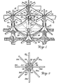
- Figure 1 shows a single photovoltaic assembly 12 partly cut away to illustrate interior details.
- Assembly 12 is adapted to be attached to adjacent, substantially identical assemblies, shown in part in Figure 1, so as to jointly form a photovoltaic array.
- Assembly 12 includes a frame structure 14 in the form of a quadrilateral right prism.
- Frame structure 14 comprises individual frames 20 which jointly define generally square top and bottom prism bases 16 and 18, respectively.
- Frames 20 individually form common partitions between adjacent PV assemblies.
- Support struts 24 and 26 are firmly attached to frame structure 14 at the respective corners of top prism base 16 by means of isolators 22, preferably consisting of a ceramic material, which electrically insulate the struts from the frame structure.
- an electrically insulating fastener 23 extends across the top of isolator 22 and fastens to a pair of frames of frame structure 14. Fastener 23 thus secures the ends of the struts which are received in isolator 22 against vertical movement, as well as fastening the aforesaid frames to the isolator.
- a cell holder 28 is supported by struts 24 and 26, as will become clear in connection with the discussion of Figure 3 below.
- a PV cell 30 is attached at one end of cell holder 28 and has a light receiving face 32 . Face 32 is oriented towards a light concentrating reflector 34 located proximate to bottom prism base 18. All the PV cell faces in the array lie substantially in a common plane parallel to and positioned between bases 16 and 18. Struts 24 and 26 support cell holder 28, and thus cell 30, within frame structure 14 such that the cell is substantially centered on an imaginary axis extending through the centers of bases 16 and 18.
- Cell 30 includes a pair of electrically conductive terminals 29 and 31 which are connected to strut sections 26b and 24b respectively. Thus, struts 26 and 24 are electrically connected to opposite polarity terminals of cell 30. Assembly 12 is shown positioned on a planar back panel 36 which underlies the entire array.
- FIG. 2 shows in greater detail the mechanical interconnection of each isolator 22 with struts 24 and 26 and with frame structure 14.
- each isolator 22 is shown to consist of an octogonal prism having a hollow cylindrical center 23.
- Each isolator 22 includes two pairs of oppositely facing, mutually aligned, blind slots 38 and 40 positioned in mutually perpendicular planes.
- Each of the blind slots is capable of receiving a frame 20 in edgewise relationship.
- each isolator is capable of receiving up to four frames, herein designated 20a, 20b, 20c and 20d.
- Isolator 22 further includes two pairs of through slots, 42 and 44, which are positioned in a pair of mutually perpendicular planes rotationally displaced by 45 * from the planes of blind slots 38 and 40.
- Each pair of through slots is adapted to receive a pair of struts endwise from opposite directions. The various components received by each isolator are securely fastened to the latter.
- a substantially rigid support structure is provided for each cell holder and for the cell held therein.
- slots 42 are shown to receive strut sections 24a and 26b, while slots 44 receive strut sections 26a and 24b.
- These four strut sections are mechanically fastened to each other inside the hollow center 23 of isolator 22, and thus they also form electrical interconnections.
- the abutting ends of the aforesaid strut sections may be brazed or otherwise soldered to each other.
- Figure 3 illustrates the arrangement of struts 24 and 26 inside the surrounding cell holder 28.
- strut 24 includes strut sections 24a and 24b on opposite sides of a bend 24c, which forms an arc of approximately 90' inside cell holder 28.
- strut 26 includes sections 26a, 26b and a bend 26c between them which also forms a 90 * arc proximate bend 24c.
- Cell 30, which is positioned on the underside of the cell holder, is shown in phantom outline in the drawing and includes light receiving surface 32 which is directed away from the viewer in Figure 3.
- a clip 25 snap fits over the top surface and a pair of opposing side walls 48 of cell holder 28, so as to firmly secure struts 24 and 26 to the cell holder.
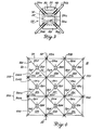
- Figure 4 schematically illustrates the mechanical and electrical interconnections of multiple assemblies 12P through 12X to form an array 10. It is to be understood that array 10 may contain more or fewer assemblies than shown and that all the assemblies are substantially identical.
- the conductive struts entering each isolator 22 are firmly held by the latter, as well as being mechanically and electrically interconnected to form a rigid structure.
- strut 24P of assembly 12P is rigidly connected at isolator 22A to strut 24Q of assembly 12Q.
- struts 24Q and 24R of assemblies 12Q and 12R respectively are rigidly interconnected at isolator 22B.
- struts 24P, 24Q and 24R jointly form an elongate rigid conductor. designated 100 in Figure 4.
- Struts 26P, 26Q and 26R jointly form a rigid conductor half 200A, while struts 24S, 24T and 24U form a rigid conductor half 200B.
- isolators 22C, 22D, 22E and 22F provide not only the electrical interconnection between struts 26 and 24 respectively, but also accomodate the interconnection of struts 26 and 24 to each other.
- conductor halves 200A and 200B together constitute a single, elongate, rigid conductor 200, as indicated in Figure 4.
- each pair of interconnected struts has opposed central bends to form a lozenge-shaped link rigidly connected to identical, adjacent links.
- array 10 includes a succession of elongate, rigid conductors 100, 200, 300, and 400, which are generally parallel to each other.
- a series of solar batteries is positioned between each pair of successive conductors.
- the term solar battery designates a photovoltaic cell, its corresponding cell holder and reflector, as well as appropriate interconnecting components.
- the batteries are preferably positioned such that successive cells of each series are aligned in a row.
- the cells indicated by cell holders 28P, 28Q and 28R form a row between the bracketing conductors 100 and 200.
- the cells of cell holders 285, 28T, and 28U are aligned in a row between the bracketing conductors 200 and 300, and the cells of cell holders 28V, 28W, and 28X form a row between the bracketing conductor pair 300 and 400.
- each row is equidistantly spaced from each other and successive cell rows are likewise spaced at equal distances from each other.
- the arrangement is such that cells in the preferred array illustrated in Figure 4 form a matrix of parallel rows and columns.
- Each cell holder 28 bridges the bracketing pairs of conductors and is firmly attached thereto to provide a substantially rigid cell support structure.
- the cells in each battery series have their terminals connected to the respective conductors of the bracketing conductor pair such that all cells in a given series are connected in parallel with each other, and the respective series of batteries are connected seriatim with each other.
- conductor 200 connects the positive terminals of all cells in the cell row indicated by cell holders 28S, 28 T , and 28U.
- Conductor 300 connects the negative terminals of the same cells.
- the cells in the aforesaid row i.e. cells held by holders 28S, 28T, and 28U, are connected in parallel with each other.
- conductor 300 connects the negative terminals of all cells in cell row 28S, 28T, and 28U with the positive terminals of all cells in the cell row constituted by cell holders 28V, 28W, and 28X.
- the two series of batteries or more specifically the two rows of cells held by holders 28S, 28T, 28U and 28V, 28W, 28X, are connected seriatim, i.e. in series with each other.
- array 10 will be positioned such that reflectors 34 face the sun, giving array 10 an anti-sun side generally defined by panel 36 and a sun-facing side as shown facing the viewer in Figure 1.
- Light incident on the respective reflectors 34 of array 10 is concentrated on light receiving faces 32 of the corresponding cells 30. Accordingly, each cell develops a voltage potential between its terminals 29 and 31.
- conductive struts 24 and 26 are connected to opposite polarity terminals of cell 30 in each assembly 12, and they are electrically interconnected at their ends to establish the aforesaid parallel and series connections of the cells in the array.
- the voltage potential of array 10 varies with the total number of the battery series connected seriatim, while the current capacity of the array varies with the number of solar batteries per series.
- a cell 30 in array 10 should fail so as to produce an open circuit, the array will continue to function at a reduced current capacity. In effect, such a cell failure will result in the removal of that cell alone from its series, thus decreasing the current capacity of that series only. If a cell 30 should develop a short circuit, one entire row of cells will be electrically shorted out. Thus, the array voltage will be reduced by the voltage of one cell.
- struts 24 and 26 provide mechanical support as well as electrical interconnections for cells 30.
- the struts, as well as frames 20 and back panel 36 are preferably constructed to be light in weight.
- the material for these components is selected to be thermally conductive and the components are configured to reject substantial amounts of heat by radiation into space, e.g. by providing large, heat-radiating surface areas.
- the thermally conductive components of the array are adapted to reject the heat from the sun-facing array side alone, i.e. without assistance from the back side of the array.
- each PV cell is seen to be positioned within its assembly such that the assembly structure substantially surrounds the cell face and shields it from externally generated particle radiation which may damage the cell.
- struts 24 and 26, frame structure 14 and back panel. 36 may all be constructed from graphite/aluminum materials which are light in weight and which provide good electrical conductivity for the struts and good thermal conductivity for the entire structure.
- Isolators 22 and cell holder 28 may be fabricated from a ceramic such as beryllium oxide, a lightweight electrical insulator.
- Cells 30 may be gallium arsenide cells and may be used in combination with segmented paraboloidal concentrating reflectors 34 made of aluminum. With such a combination of materials, a lightweight structure may be constructed which is readily deployable in space and which is more efficient and provides a substantially higher electrical output in absolute voltage and current capacity than similarly sized, conventional, planar silicon cell arrays without concentrators.
- terminals 29 and 31 may be augmented with redundant pairs of similarly connected terminals, preventing an open circuit fault if one of the terminals should fail.
Abstract
Description
- The present invention relates in general to a solar battery array and in particular to an array of photovoltaic assemblies including photovoltaic cells and light concentrating reflectors.
- The use of light concentrating reflectors in a photovoltaic (PV) cell array has the advantage of increasing the efficiency of the PV cell operation, while decreasing the cost per unit of generated power output through the substitution of relatively low cost reflector material for relatively high cost photovoltaic cell material. Meeting both the electrical and thermal requirements of such a concentrating array is, however, a complex and formidable problem. While various methods of interconnecting PV cells into arrays are known in the art, these arrays generally require the use of separate apparatus for mechanically supporting and electrically interconnecting the cells. Not only is the assembly of such apparatus an often intricate, time-consuming and expensive process, but most of these arrays have the further drawback of necessitating the use of heat damageable materials. For example, heat sensitive polymeric wire insulation is often required. Further, heat sensitive adhesive is often used to secure protective cover glass to the PV cell faces. Thus, many of the currently available arrays will not function in a high heat environment which may include externally generated heat-producing particle radiation.
- Those prior art arrays which use light concentrating reflectors generally require bulky, intricate, and often unwieldy cooling equipment. For example, U.S. patent 4,361,717 shows the use of a concentrating reflector in an array which requires a complicated fluid cooling system to dissipate heat. Such a cooling system increases the complexity and weight of the overall array and complicates its assembly, especially when the array is deployed in space. Further, such a cooling system increases the expense of the array.
- When it is desired to maximize array protection from particle radiation, it may be necessary to provide special shielding for the side of the array which faces away from the sun. Under these conditions, the heat rejection capability of the anti-sun side is lost and heat rejection depends on the sun-facing side of the array alone. Thus, the demands made of the cooling equipment are increased, requiring still bulkier and more expensive apparatus.
- It is a principal object of the present invention to provide a new and improved PV cell array which is not subject to the aforementioned problems and disadvantages.
- Another object of the present invention is to provide a PV cell array which uses light concentrating reflectors to increase the efficiency of the PV cells.
- A further object of the present invention is to provide a PV cell array which can utilize light concentrating reflectors without requiring complicated or unwieldy heat dissipation apparatus and which can, with minimal degradation in performance, withstand high transient temperatures such as may be induced by externally generated particle radiation.
- A further object of the present invention is to provide a PV cell array which does not require the use of separate structures for supporting and electrically interconnecting the PV cells in the array.
- Yet another object of the present invention is to provide a PV cell array which does not require the use of heat damageable materials, such as polymeric electrical wire insulation or cover glass adhesive, in its construction.
- A further object of the present invention is to provide apparatus for easily and simply interconnecting a plurality of PV cells in an array.
- Another object of the present invention is to provide a new and improved photovoltaic assembly which can be easily and quickly combined with identical assemblies to form a relatively inexpensive array of assemblies.
- Yet another object of the present invention is to provide a new and improved PV assembly which can provide the necessary heat rejection for the entire array from the sun-facing array side alone.
- A further object of the present invention is to provide a new and improved PV assembly wherein the cells are positioned within the array so as to receive maximum protection from external particle radiation.
- The foregoing and other objects of the present invention are achieved through the use of a new and improved photovoltaic assembly having a light concentrating reflector, which can be quickly combined with identical assemblies to form a solar battery array. In the array the electrical interconnection of the cells is accomplished by the cell support structure. Specifically, a combination of electrical conductors and electrical insulating elements is used to support each cell at the focal point of its reflector, the latter being spaced from the cell. The conductors are connected to the cells and interconnected to each other in a manner which provides both the desired series and parallel electrical connection of the cells.
- The cell support structure, in conjunction with the remainder of the array, is configured to reject heat by dissipation into space. This occurs from the sun-facing side of the array alone, where the anti-sun side of the array is shrouded by a panel, e.g. for protection against external particle radiation. Further, the PV cells are positioned within the array in a manner whereby they are shielded from externally generated particle radiation.
-
- Figure 1 is a perspective view of a preferred embodiment of the invention, showing a single assembly partially cut away to illustrate interior details.
- Figure 2 is a cross-sectional plan view.of an isolator and associated structure depicted in Figure 1.
- Figure 3 is a plan view of the cell holder depicted in Figure 1, partly cut-away for purposes of illustration.
- Figure 4 is a plan view of an array of assemblies of arbitrary size in accordance with the present invention, shown partly in schematic form, with portions omitted for the sake of clarity.
- Detailed Description of the Drawings
- Referring now to the drawings, Figure 1 shows a single
photovoltaic assembly 12 partly cut away to illustrate interior details.Assembly 12 is adapted to be attached to adjacent, substantially identical assemblies, shown in part in Figure 1, so as to jointly form a photovoltaic array.Assembly 12 includes a frame structure 14 in the form of a quadrilateral right prism. Frame structure 14 comprisesindividual frames 20 which jointly define generally square top andbottom prism bases Frames 20 individually form common partitions between adjacent PV assemblies. - A first electrically
conductive support strut 24, consisting ofstrut sections top prism base 16 towards the center of the base. Similarly, a second support strut 26, consisting ofstrut sections base 16 towards the center of the base.Support struts 24 and 26 are firmly attached to frame structure 14 at the respective corners oftop prism base 16 by means ofisolators 22, preferably consisting of a ceramic material, which electrically insulate the struts from the frame structure. At each corner ofbase 16, an electrically insulatingfastener 23 extends across the top ofisolator 22 and fastens to a pair of frames of frame structure 14.Fastener 23 thus secures the ends of the struts which are received inisolator 22 against vertical movement, as well as fastening the aforesaid frames to the isolator. - A
cell holder 28 is supported bystruts 24 and 26, as will become clear in connection with the discussion of Figure 3 below. APV cell 30 is attached at one end ofcell holder 28 and has alight receiving face 32 .Face 32 is oriented towards alight concentrating reflector 34 located proximate tobottom prism base 18. All the PV cell faces in the array lie substantially in a common plane parallel to and positioned betweenbases Struts 24 and 26support cell holder 28, and thuscell 30, within frame structure 14 such that the cell is substantially centered on an imaginary axis extending through the centers ofbases -
Cell 30 includes a pair of electricallyconductive terminals strut sections struts 26 and 24 are electrically connected to opposite polarity terminals ofcell 30.Assembly 12 is shown positioned on aplanar back panel 36 which underlies the entire array. - Figure 2 shows in greater detail the mechanical interconnection of each
isolator 22 withstruts 24 and 26 and with frame structure 14. In the illustrated embodiment of the invention, eachisolator 22 is shown to consist of an octogonal prism having a hollowcylindrical center 23. Eachisolator 22 includes two pairs of oppositely facing, mutually aligned,blind slots frame 20 in edgewise relationship. As shown in Figure 2, each isolator is capable of receiving up to four frames, herein designated 20a, 20b, 20c and 20d. -
Isolator 22 further includes two pairs of through slots, 42 and 44, which are positioned in a pair of mutually perpendicular planes rotationally displaced by 45* from the planes ofblind slots - In Figure 2,
slots 42 are shown to receivestrut sections slots 44 receivestrut sections hollow center 23 ofisolator 22, and thus they also form electrical interconnections. By way of example and without limitation, the abutting ends of the aforesaid strut sections may be brazed or otherwise soldered to each other. - Figure 3 illustrates the arrangement of
struts 24 and 26 inside the surroundingcell holder 28. As shown, strut 24 includesstrut sections inside cell holder 28. Similarly, strut 26 includessections Cell 30, which is positioned on the underside of the cell holder, is shown in phantom outline in the drawing and includeslight receiving surface 32 which is directed away from the viewer in Figure 3. Aclip 25 snap fits over the top surface and a pair of opposingside walls 48 ofcell holder 28, so as to firmlysecure struts 24 and 26 to the cell holder. - Figure 4 schematically illustrates the mechanical and electrical interconnections of
multiple assemblies 12P through 12X to form anarray 10. It is to be understood thatarray 10 may contain more or fewer assemblies than shown and that all the assemblies are substantially identical. As explained above, the conductive struts entering each isolator 22 are firmly held by the latter, as well as being mechanically and electrically interconnected to form a rigid structure. Thus, strut 24P ofassembly 12P is rigidly connected at isolator 22A to strut 24Q ofassembly 12Q. Similarly, struts 24Q and 24R ofassemblies -
Struts rigid conductor half 200A, whilestruts 24S, 24T and 24U form arigid conductor half 200B. It will be noted that isolators 22C, 22D, 22E and 22F provide not only the electrical interconnection betweenstruts 26 and 24 respectively, but also accomodate the interconnection ofstruts 26 and 24 to each other. Thus, conductor halves 200A and 200B together constitute a single, elongate,rigid conductor 200, as indicated in Figure 4. As shown, each pair of interconnected struts has opposed central bends to form a lozenge-shaped link rigidly connected to identical, adjacent links. Similarly, struts 26S, 26T, and 26U and struts 24V, 24W, and 24X form conductor halves 300A and 300B respectively, which jointly constituteconductor 300.Struts 26V, 26W and 26X jointly formconductor 400. Thus,array 10 includes a succession of elongate,rigid conductors - A series of solar batteries is positioned between each pair of successive conductors. As used herein, the term solar battery designates a photovoltaic cell, its corresponding cell holder and reflector, as well as appropriate interconnecting components. The batteries are preferably positioned such that successive cells of each series are aligned in a row. Thus, the cells indicated by
cell holders conductors cell holders conductors cell holders conductor pair cell holder 28 bridges the bracketing pairs of conductors and is firmly attached thereto to provide a substantially rigid cell support structure. - As schematically indicated by the "+" and "-" polarities in Figure 4, the cells in each battery series have their terminals connected to the respective conductors of the bracketing conductor pair such that all cells in a given series are connected in parallel with each other, and the respective series of batteries are connected seriatim with each other. For example,
conductor 200 connects the positive terminals of all cells in the cell row indicated bycell holders Conductor 300 connects the negative terminals of the same cells. Thus, the cells in the aforesaid row, i.e. cells held byholders conductor 300 connects the negative terminals of all cells incell row cell holders holders array 10, it will become apparent that the total voltage of the array appears between apositive array terminal 50 and a negative array terminal 52, shown connected at isolators 22A and 22L respectively. - In operation,
array 10 will be positioned such thatreflectors 34 face the sun, givingarray 10 an anti-sun side generally defined bypanel 36 and a sun-facing side as shown facing the viewer in Figure 1. Light incident on therespective reflectors 34 ofarray 10 is concentrated on light receiving faces 32 of the correspondingcells 30. Accordingly, each cell develops a voltage potential between itsterminals conductive struts 24 and 26 are connected to opposite polarity terminals ofcell 30 in eachassembly 12, and they are electrically interconnected at their ends to establish the aforesaid parallel and series connections of the cells in the array. Thus, the voltage potential ofarray 10 varies with the total number of the battery series connected seriatim, while the current capacity of the array varies with the number of solar batteries per series. - If a
cell 30 inarray 10 should fail so as to produce an open circuit, the array will continue to function at a reduced current capacity. In effect, such a cell failure will result in the removal of that cell alone from its series, thus decreasing the current capacity of that series only. If acell 30 should develop a short circuit, one entire row of cells will be electrically shorted out. Thus, the array voltage will be reduced by the voltage of one cell. - An important feature of the present invention is that certain structural elements of
array 10, i.e. struts 24 and 26, provide mechanical support as well as electrical interconnections forcells 30. The struts, as well asframes 20 and backpanel 36 are preferably constructed to be light in weight. Further, the material for these components is selected to be thermally conductive and the components are configured to reject substantial amounts of heat by radiation into space, e.g. by providing large, heat-radiating surface areas. In accordance with the present invention, the thermally conductive components of the array are adapted to reject the heat from the sun-facing array side alone, i.e. without assistance from the back side of the array. Further, each PV cell is seen to be positioned within its assembly such that the assembly structure substantially surrounds the cell face and shields it from externally generated particle radiation which may damage the cell. - By way of example but without limitation, struts 24 and 26, frame structure 14 and back panel. 36 may all be constructed from graphite/aluminum materials which are light in weight and which provide good electrical conductivity for the struts and good thermal conductivity for the entire structure.
Isolators 22 andcell holder 28 may be fabricated from a ceramic such as beryllium oxide, a lightweight electrical insulator.Cells 30 may be gallium arsenide cells and may be used in combination with segmentedparaboloidal concentrating reflectors 34 made of aluminum. With such a combination of materials, a lightweight structure may be constructed which is readily deployable in space and which is more efficient and provides a substantially higher electrical output in absolute voltage and current capacity than similarly sized, conventional, planar silicon cell arrays without concentrators. - While a preferred embodiment of the invention has been described and illustrated, it will be obvious to those skilled in the art that the invention is not so limited. For example, the configuration of the back panel described and illustrated herein may be altered or the panel may be omitted altogether. Further,
terminals - While the preferred embodiment illustrated herein comprises specific materials and mechanical structures, it will be obvious to those skilled in the art that many variations and substitutions are possible within the purview of the invention as to the materials employed, the physical shape of the structural elements, and the specific interconnection of the respective elements. Thus, numerous modifications, changes, variations, substitutions and equivalents, in whole or in part, will now occur to those skilled in the art without departing from the spirit and scope of the invention. Accordingly, it is intended that the invention herein be limited only by the scope of the appended claims.
Claims (19)
each of said cell holders being fastened to a pair of said proximate central bends of a bracketing pair of conductors.
Applications Claiming Priority (2)
| Application Number | Priority Date | Filing Date | Title |
|---|---|---|---|
| US06/669,082 US4604494A (en) | 1984-11-07 | 1984-11-07 | Photovoltaic cell array with light concentrating reflectors |
| US669082 | 2000-09-25 |
Publications (2)
| Publication Number | Publication Date |
|---|---|
| EP0180877A2 true EP0180877A2 (en) | 1986-05-14 |
| EP0180877A3 EP0180877A3 (en) | 1987-07-15 |
Family
ID=24684936
Family Applications (1)
| Application Number | Title | Priority Date | Filing Date |
|---|---|---|---|
| EP85113647A Withdrawn EP0180877A3 (en) | 1984-11-07 | 1985-10-26 | Photovoltaic cell array with light concentrating device |
Country Status (4)
| Country | Link |
|---|---|
| US (1) | US4604494A (en) |
| EP (1) | EP0180877A3 (en) |
| JP (1) | JPS61119081A (en) |
| CN (1) | CN85108094A (en) |
Cited By (4)
| Publication number | Priority date | Publication date | Assignee | Title |
|---|---|---|---|---|
| EP0373234A1 (en) * | 1988-12-12 | 1990-06-20 | Siemens Aktiengesellschaft | Solar generator |
| CN102386278A (en) * | 2011-10-21 | 2012-03-21 | 无锡绿波新能源设备有限公司 | Quick switching device for quickly switching polycrystalline chip carrying device to monocrystalline chip carrying device |
| WO2014021948A1 (en) * | 2012-07-31 | 2014-02-06 | Semprius, Inc. | Surface-mountable lens cradles and interconnection structures for concentrator-type photovoltaic devices |
| EP2806468A1 (en) * | 2013-05-24 | 2014-11-26 | Universidad Politécnica de Madrid | Photovoltaic receiver for solar concentrator |
Families Citing this family (42)
| Publication number | Priority date | Publication date | Assignee | Title |
|---|---|---|---|---|
| US5212916A (en) * | 1984-07-26 | 1993-05-25 | Peter Raupach | Device for shading spaces |
| US4716258A (en) * | 1987-01-23 | 1987-12-29 | Murtha R Michael | Stamped concentrators supporting photovoltaic assemblies |
| US5374317A (en) | 1990-09-26 | 1994-12-20 | Energy Systems Solar, Incorporated | Multiple reflector concentrator solar electric power system |
| US5086828A (en) * | 1991-09-25 | 1992-02-11 | The United States Of America As Represented By The Administrator Of The National Aeronautics And Space Administration | Lunar radiator shade |
| US5632032A (en) * | 1994-02-07 | 1997-05-20 | International Business Machines Corporation | Cross address space thread control in a multithreaded environment |
| US8577839B2 (en) * | 2002-08-06 | 2013-11-05 | Sheng Tai (Ted) Tsao | Method and apparatus of dynamic updating web portals |
| US20060243319A1 (en) * | 2005-04-29 | 2006-11-02 | Arizona Public Service Company | Clustered solar-energy conversion array and method therefor |
| US7622666B2 (en) * | 2005-06-16 | 2009-11-24 | Soliant Energy Inc. | Photovoltaic concentrator modules and systems having a heat dissipating element located within a volume in which light rays converge from an optical concentrating element towards a photovoltaic receiver |
| US20070089777A1 (en) * | 2005-10-04 | 2007-04-26 | Johnson Richard L Jr | Heatsink for concentrating or focusing optical/electrical energy conversion systems |
| WO2007044385A2 (en) * | 2005-10-04 | 2007-04-19 | Practical Instruments, Inc. | Self-powered systems and methods using auxiliary solar cells |
| EP1989492A2 (en) * | 2006-01-17 | 2008-11-12 | Soliant Energy, Inc. | Concentrating solar panel and related systems and methods |
| WO2007084518A2 (en) * | 2006-01-17 | 2007-07-26 | Soliant Energy, Inc. | A hybrid primary optical component for optical concentrators |
| JP4863792B2 (en) * | 2006-07-05 | 2012-01-25 | 日軽金アクト株式会社 | Solar power plant |
| WO2008039510A1 (en) * | 2006-09-30 | 2008-04-03 | Soliant Energy, Inc. | Optical concentrators having one or more spot focus and related methods |
| WO2008048478A2 (en) * | 2006-10-13 | 2008-04-24 | Soliant Energy, Inc. | Sun sensor assembly and related method of using |
| US20090000662A1 (en) * | 2007-03-11 | 2009-01-01 | Harwood Duncan W J | Photovoltaic receiver for solar concentrator applications |
| WO2008113837A2 (en) * | 2007-03-20 | 2008-09-25 | Lemnis Lighting Patent Holding B.V. | Heat management system for photovoltaic cell panels and led-based light sources |
| US20100269428A1 (en) * | 2007-05-23 | 2010-10-28 | Robert Stancel | Cost Effective, Elongate Member Mounting System For Photovoltaic Devices |
| US20090114213A1 (en) * | 2007-11-03 | 2009-05-07 | Solfocus, Inc. | Solar concentrator with square mirrors |
| US8748727B2 (en) | 2008-01-18 | 2014-06-10 | Tenksolar, Inc. | Flat-plate photovoltaic module |
| US20090183764A1 (en) * | 2008-01-18 | 2009-07-23 | Tenksolar, Inc | Detachable Louver System |
| US8933320B2 (en) | 2008-01-18 | 2015-01-13 | Tenksolar, Inc. | Redundant electrical architecture for photovoltaic modules |
| US8212139B2 (en) | 2008-01-18 | 2012-07-03 | Tenksolar, Inc. | Thin-film photovoltaic module |
| GB2471818B (en) * | 2008-05-12 | 2013-03-20 | Univ Arizona | Method of manufacturing large dish reflectors for a solar concentrator apparatus |
| US20110094563A9 (en) | 2008-05-16 | 2011-04-28 | Baker James T | Solar systems that include one or more shade-tolerant wiring schemes |
| WO2010000108A1 (en) * | 2008-07-01 | 2010-01-07 | Yingtian Chen | Concentrating photovoltaic cell system, wiring and aranging methods thereof |
| US20100018009A1 (en) * | 2008-07-22 | 2010-01-28 | Solfocus, Inc. | Clips for Aligning Optical Components in a Solar Concentrating Array |
| US8664514B2 (en) * | 2008-10-13 | 2014-03-04 | George M. Watters | Multiplexing solar light chamber |
| EP2443666A4 (en) | 2009-06-15 | 2013-06-05 | Tenksolar Inc | Illumination agnostic solar panel |
| US9605877B2 (en) * | 2010-02-10 | 2017-03-28 | Edward Wu | Compact parabolic solar concentrators and cooling and heat extraction system |
| US9773933B2 (en) | 2010-02-23 | 2017-09-26 | Tenksolar, Inc. | Space and energy efficient photovoltaic array |
| US9299861B2 (en) | 2010-06-15 | 2016-03-29 | Tenksolar, Inc. | Cell-to-grid redundandt photovoltaic system |
| EP2603932A4 (en) | 2010-08-10 | 2017-07-05 | Tenksolar, Inc. | Highly efficient solar arrays |
| US9893223B2 (en) | 2010-11-16 | 2018-02-13 | Suncore Photovoltaics, Inc. | Solar electricity generation system |
| US9528724B1 (en) | 2011-06-08 | 2016-12-27 | Solarreserve Technology, Llc | Apparatus and method for configuring heliostat fields |
| WO2014085436A1 (en) | 2012-11-30 | 2014-06-05 | Arizona Board Of Regents On Behalf Of University Of Arizona | Solar generator with large reflector dishes and concentrator photovoltaic cells in flat arrays |
| US9746127B2 (en) | 2013-10-22 | 2017-08-29 | The Arizona Board Of Regents On Behalf Of The University Of Arizona | Frame with compression and tension members to rotate equipment about an axis |
| EP2958155B1 (en) * | 2014-06-20 | 2016-10-19 | Vismunda S.r.l. | Plant and system for the automatic horizontal assembly of photovoltaic panels with front-back connection of the cells and pre-fixing |
| US10505059B2 (en) | 2015-01-16 | 2019-12-10 | The Arizona Board Of Regents On Behalf Of The University Of Arizona | Micro-scale concentrated photovoltaic module |
| WO2016141041A1 (en) | 2015-03-02 | 2016-09-09 | The Arizona Board Of Regents On Behalf Of The University Of Arizona | Glass forming mold of adjustable shape |
| WO2016200988A1 (en) | 2015-06-12 | 2016-12-15 | The Arizona Board Of Regents On Behalf Of The University Of Arizona | Tandem photovoltaic module with diffractive spectral separation |
| WO2017024038A1 (en) | 2015-08-03 | 2017-02-09 | The Arizona Board Of Regents On Behalf Of The University Of Arizona | Solar concentrator for a tower-mounted central receiver |
Citations (3)
| Publication number | Priority date | Publication date | Assignee | Title |
|---|---|---|---|---|
| US3658596A (en) * | 1970-09-21 | 1972-04-25 | Lockheed Missiles Space | Flexible solar cell modular assembly |
| US3819417A (en) * | 1972-05-17 | 1974-06-25 | Communications Satellite Corp | Mechanically interlaced and electrically interconnected silicon solar cells |
| FR2353091A1 (en) * | 1976-05-26 | 1977-12-23 | Massachusetts Inst Technology | SOLAR RADIATION COLLECTOR |
Family Cites Families (5)
| Publication number | Priority date | Publication date | Assignee | Title |
|---|---|---|---|---|
| US3459391A (en) * | 1964-02-13 | 1969-08-05 | Nasa | Interconnection of solar cells |
| US3446676A (en) * | 1966-09-07 | 1969-05-27 | Webb James E | Solar battery with interconnecting means for plural cells |
| US3756858A (en) * | 1970-09-14 | 1973-09-04 | Trw Inc | Folding thin-film deployable panel structure |
| US3984256A (en) * | 1975-04-25 | 1976-10-05 | Nasa | Photovoltaic cell array |
| US4361717A (en) * | 1980-12-05 | 1982-11-30 | General Electric Company | Fluid cooled solar powered photovoltaic cell |
-
1984
- 1984-11-07 US US06/669,082 patent/US4604494A/en not_active Expired - Fee Related
-
1985
- 1985-05-16 CN CN198585108094A patent/CN85108094A/en active Pending
- 1985-10-26 EP EP85113647A patent/EP0180877A3/en not_active Withdrawn
- 1985-11-01 JP JP60244273A patent/JPS61119081A/en active Pending
Patent Citations (3)
| Publication number | Priority date | Publication date | Assignee | Title |
|---|---|---|---|---|
| US3658596A (en) * | 1970-09-21 | 1972-04-25 | Lockheed Missiles Space | Flexible solar cell modular assembly |
| US3819417A (en) * | 1972-05-17 | 1974-06-25 | Communications Satellite Corp | Mechanically interlaced and electrically interconnected silicon solar cells |
| FR2353091A1 (en) * | 1976-05-26 | 1977-12-23 | Massachusetts Inst Technology | SOLAR RADIATION COLLECTOR |
Cited By (5)
| Publication number | Priority date | Publication date | Assignee | Title |
|---|---|---|---|---|
| EP0373234A1 (en) * | 1988-12-12 | 1990-06-20 | Siemens Aktiengesellschaft | Solar generator |
| CN102386278A (en) * | 2011-10-21 | 2012-03-21 | 无锡绿波新能源设备有限公司 | Quick switching device for quickly switching polycrystalline chip carrying device to monocrystalline chip carrying device |
| WO2014021948A1 (en) * | 2012-07-31 | 2014-02-06 | Semprius, Inc. | Surface-mountable lens cradles and interconnection structures for concentrator-type photovoltaic devices |
| EP2806468A1 (en) * | 2013-05-24 | 2014-11-26 | Universidad Politécnica de Madrid | Photovoltaic receiver for solar concentrator |
| WO2014187975A1 (en) * | 2013-05-24 | 2014-11-27 | Universidad Politécnica de Madrid | Solar cell receiver suitable for reflective solar concentrator modules |
Also Published As
| Publication number | Publication date |
|---|---|
| CN85108094A (en) | 1986-10-01 |
| JPS61119081A (en) | 1986-06-06 |
| EP0180877A3 (en) | 1987-07-15 |
| US4604494A (en) | 1986-08-05 |
Similar Documents
| Publication | Publication Date | Title |
|---|---|---|
| US4604494A (en) | Photovoltaic cell array with light concentrating reflectors | |
| US4433200A (en) | Roll formed pan solar module | |
| ES2360614T3 (en) | PHOTOVOLTAIC MODULES AND INTERCONNECTION METHODOLOGY TO MANUFACTURE THEMSELVES. | |
| JP4705366B2 (en) | Solar generator panels and related satellites | |
| US4834805A (en) | Photovoltaic power modules and methods for making same | |
| EP0581889B1 (en) | Generating electric power from solar radiation | |
| US3340096A (en) | Solar cell array | |
| US4153476A (en) | Double-sided solar cell package | |
| EP0017334A1 (en) | Solar panel module | |
| US20100275976A1 (en) | Photovoltaic module with edge access to pv strings, interconnection method, apparatus, and system | |
| SG176193A1 (en) | Photovoltaic module string arrangement and shading protection therefor | |
| US4209347A (en) | Mounting for solar cell | |
| CN111403491A (en) | Sliced cell photovoltaic module | |
| JP2003242956A (en) | Battery module | |
| US11600733B2 (en) | System and method for shingling wafer strips connected in parallel | |
| CN107810599B (en) | Terminal for solar junction box | |
| US4131755A (en) | Interconnection for photovoltaic device array | |
| US4162174A (en) | Solar cell array | |
| US3466198A (en) | Solar cell matrix | |
| US4153475A (en) | Three dimensional solar panel assembly | |
| RU2053937C1 (en) | Space vehicle | |
| JP2000036329A (en) | Three-dimensional battery applicable to space | |
| JP3106778B2 (en) | Solar cell module | |
| JPH03104174A (en) | Solar battery power supply equipment | |
| WO2023217908A1 (en) | Photovoltaic module with shade-tolerant cell-string layout |
Legal Events
| Date | Code | Title | Description |
|---|---|---|---|
| PUAI | Public reference made under article 153(3) epc to a published international application that has entered the european phase |
Free format text: ORIGINAL CODE: 0009012 |
|
| AK | Designated contracting states |
Kind code of ref document: A2 Designated state(s): DE FR GB IT NL SE |
|
| PUAL | Search report despatched |
Free format text: ORIGINAL CODE: 0009013 |
|
| AK | Designated contracting states |
Kind code of ref document: A3 Designated state(s): DE FR GB IT NL SE |
|
| 17P | Request for examination filed |
Effective date: 19880107 |
|
| STAA | Information on the status of an ep patent application or granted ep patent |
Free format text: STATUS: THE APPLICATION IS DEEMED TO BE WITHDRAWN |
|
| 18D | Application deemed to be withdrawn |
Effective date: 19900501 |
|
| RIN1 | Information on inventor provided before grant (corrected) |
Inventor name: SHEPARD, NEAL FRANKLIN, JR. |