EP0180196B1 - Programmable counter/timer device - Google Patents
Programmable counter/timer device Download PDFInfo
- Publication number
- EP0180196B1 EP0180196B1 EP85113745A EP85113745A EP0180196B1 EP 0180196 B1 EP0180196 B1 EP 0180196B1 EP 85113745 A EP85113745 A EP 85113745A EP 85113745 A EP85113745 A EP 85113745A EP 0180196 B1 EP0180196 B1 EP 0180196B1
- Authority
- EP
- European Patent Office
- Prior art keywords
- counter
- register
- timer
- task
- task instruction
- Prior art date
- Legal status (The legal status is an assumption and is not a legal conclusion. Google has not performed a legal analysis and makes no representation as to the accuracy of the status listed.)
- Expired - Lifetime
Links
Images


Classifications
-
- G—PHYSICS
- G06—COMPUTING; CALCULATING OR COUNTING
- G06F—ELECTRIC DIGITAL DATA PROCESSING
- G06F7/00—Methods or arrangements for processing data by operating upon the order or content of the data handled
-
- G—PHYSICS
- G04—HOROLOGY
- G04G—ELECTRONIC TIME-PIECES
- G04G99/00—Subject matter not provided for in other groups of this subclass
- G04G99/006—Electronic time-pieces using a microcomputer, e.g. for multi-function clocks
-
- G—PHYSICS
- G04—HOROLOGY
- G04G—ELECTRONIC TIME-PIECES
- G04G15/00—Time-pieces comprising means to be operated at preselected times or after preselected time intervals
- G04G15/006—Time-pieces comprising means to be operated at preselected times or after preselected time intervals for operating at a number of different times
-
- G—PHYSICS
- G06—COMPUTING; CALCULATING OR COUNTING
- G06F—ELECTRIC DIGITAL DATA PROCESSING
- G06F9/00—Arrangements for program control, e.g. control units
- G06F9/06—Arrangements for program control, e.g. control units using stored programs, i.e. using an internal store of processing equipment to receive or retain programs
- G06F9/22—Microcontrol or microprogram arrangements
Description
- The present invention relates to a counter/timer device, and more particularly to a programmable counter/timer device in which a counter/timer register and a capture/compare register both used for a timing operation can be freely selected from a register group made up of a plurality of registers.
- In a conventional counter/timer LSI which is fabricated for and connected to a microcomputer, a single capture register and a single compare register are usually provided for each of a plurality of counter/timer registers, and it is impossible to change the functions of these registers. Further, an input terminal for applying a control signal from the outside to a counter/timer and an output terminal for delivering an output from the counter/timer to the outside are connected only to the counter/timer, and it is impossible to connect the input and output terminals to another counter/ timer. Furthermore, a control register, through which a central processing unit sets the function of counter/timer register, is provided for each counter/timer register. For example, in the MC 6840 which is manufactured by the Motorola Inc. and is a typical counter/timer LSI, three counter/ timer registers are provided, and one capture register, one control register, two input terminals and one output terminals are provided for each of the counter/timer registers. In the MC 6840, however, the contents of each counter/timer register are always compared with zero, and hence a compare register is absent in the strict sense. Further, the arrangement of these registers and input/output terminals is fixed.
- While, a counter/timer incorporated in a single-chip microcomputer is discussed in, for example, an article entitled "Motorola's MC68HC11: Definition and Design of a VLSI Microcomputer" by J.M. Sibigtroth (IEEE MICRO, February, 1984). The single-chip microcomputer discussed in the above article has an excellent function. In this microcomputer, however, the number of counter/ timer registers, the number of capture registers each for holding the number of input pulses, and the number of compare registers each for determining a time interval between pulsive outputs are all fixed. Moreover, the functions of these registers as well as the combination of counter/ timer registers and capture/compare registers are fixed. Accordingly, in a case where the single-chip microcomputer is applied to the control of various apparatuses, the counter/timer part of the microcomputer will be deficient in the selection of registers. Further, as to the arrangement of 1/O pins, only the output terminal of a specified counter/timer register can be selected from a plurality of terminals, but other terminals are fixed. Specifically, in a single-chip microcomputer, the number of I/0 terminals is limited, and hence it is desirable to be able to freely change the connection between counter/timer registers and I/O terminals.
- An object of the present invention is to provide a programmable counter/timer device in which the number of counter/timer registers, the number of capture registers and the number of compare registers can be freely changed, in order for the device to be used for controlling various apparatuses.
- A characteristic feature of the present invention resides in that a counter/timer register, a capture register and a compare register are freely selected from a plurality of registers provided in a counter/ timer device. Further, another characteristic feature of the present invention resides in that unlike the conventional counter/timer in which the control register is provided for each counter/ timer register, a task register is provided for eaoh of tasks for controlling input and output processing, and a task instruction for selecting registers used as a counter/timer register, a capture register and a compare register, specifying the functions of the selected registers at the task concerned, and specifying input and output terminals, is written in the task register. Task registers in a counter/timer device are scanned to successively process the tasks, and thus the task instructions written in the task registers are executed at once.
- The present invention will be more apparent from the following detailed description of a preferred embodiment taken in conjunction with the accompanying drawings, in which:
- Fig. 1 is a block diagram showing an embodiment of a single-chip microcomputer, to which the present invention is applied;
- Fig. 2 is a block diagram showing a counter/ timer unit according to the present invention, which is included in the single-chip microcomputer of Fig. 1;
- Fig. 3 is a schematic diagram showing the format of a task instruction used in the counter/ timer unit of Fig. 2;
- Fig. 4 is a timing chart showing the timing of operation in the counter/timer unit of Fig. 2;
- Fig. 5 is a schematic diagram showing the format of a task instruction for specifying a first processing example;
- Fig. 6 is a waveform chart for explaining the execution of the task instruction given by the format of Fig. 5;
- Fig. 7 is schematic diagram showing the format of a task instruction for specifying a second processing example;
- Fig. 8 is a waveform chart for explaining the execution of the task instruction given by the format of Fig. 7;
- Fig. 9 is a schematic diagram showing the format of a task instruction for specifying a third processing example;
- Fig. 10 is a waveform chart for explaining the execution of the task instruction given by the format of Fig. 9;
- Fig. 11 is a schematic diagram showing the format of a task instruction for specifying a fourth processing example; and
- Fig. 12 is a waveform chart for explaining the execution of the task instruction given by the format of Fig. 11.
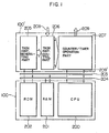
- Fig. 1 shows the outline of an embodiment of a single-chip microcomputer, to which the present invention is applied. Referring to Fig. 1, a
microcomputer unit 100 is made up of a CPU (namely, a central processing unit) 200, aRAM 201 serving as a data storage part, and aROM 202 serving as a program storage part. Further, a counter/timer unit 100' is made up of a taskinstruction generating part 205, a taskinstruction control part 206 and a counter/timer operation part 207. Themicrocomputer unit 100 is connected to the counter/timer unit 100' through adata bus 203 and an address/control bus 204. - The task
instruction generating part 205 is formed mainly of a register group which stores task instructions for specifying registers and input/output terminals used in each task and for specifying the operation mode of each of the specified registers. In the embodiment of Fig. 1, the task instructions are sent from themicrocomputer unit 100 to the taskinstruction generating part 205 through thedata bus 203, to be stored in the register group. However, in a case where tasks to be carried out in the counter/timer unit 100' have been previously determined, task instructions for carrying out the above tasks may be previously stored in a ROM (namely, a read only memory), at need. Further, this ROM may be a ROM whose contents can be altered, such as an erasable and programmable ROM or an electrically erasable and programmable ROM. The task instructions written in the taskinstruction generating part 205 are successively read out in a predetermined order, and sent to the counter/timer operation part 207 through the taskinstruction control part 206, to control thepart 207. Thus, all of the task instructions are executed at once. Incidentally, in Fig. 1,reference numeral 208 designates an input terminal group for supplying a control signal from the outside to the taskinstruction control part timer operation part 207, to the outside and themicrocomputer unit 100. - The task
instruction control part 206 generates a decoded signal for controlling the operating order and operation modes of constituent elements of the counter/timer operation part 207 in synchronism with an internal clock signal, on the basis of a task instruction from the taskinstruction generating part 205 and a control signal from theinput terminal group 208. - The counter/
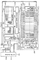
timer operation part 207 performs various operations such as mentioned below. That is, in thepart 207, a counter/timer register is incremented to perform a counter/timer function, the contents of a counter/timer register are transferred to a capture register, the contents of a counter/timer register are compared with the contents of a compare register, an output signal is delivered to theoutput terminal group 209, and so on. - Fig. 2 shows, in block, the detailed construction of the counter/timer unit 100'. Referring to Fig. 2, the task
instruction generating part 205 includes a tasksignal generating circuit 101 which is formed of a counter in the present embodiment, atask address decoder 102, and atask register group 103 which is made up of sixteen task registers in the present embodiment. In order to control various apparatus connected externally to the single-chip microcomputer, it is necessary to carry out a large number of input/output processing tasks. In the prior art, at least one register set made up of a counter/timer register, a capture register, a compare register, a control register, an input terminal and an output terminal is selected for each processing task, and a central processing unit specifies the operation mode of the selected counter/timer register through the control register. In this case, however, the capture or compare register and the input or output terminal included in the selected register set may become useless depending upon the contents of the task, and thus the prior art involves waste. - While, according to the present invention, a number of task instructions are stored in the
task register group 103, and task numbers are successively generated by the tasksignal generating circuit 101. The task numbers are supplied to thetask register group 103 through thetask address decoder 102, to read out a task instruction from a task register corresponding to a task number specified by the tasksignal generating circuit 101 and to execute the read-out task instruction. - In the present embodiment, each task instruction, as shown in Fig. 3, is formed of 31 bits and includes a task number of 4 bits, an input or output specifying bit of one bit, a counter/timer register number of 4 bits, a capture/compare register number of 4 bits, a conditions in counting operation given by 3 bits, conditions in capture/ compare operation given by 3 bits, a clock input pin number of 4 bits, a capture/reset signal input pin number of 4 bits, and an output pin number of 4 bits. The task instruction read out from the task register is applied to an
operation control decoder 104, to generate acontrol signal 113 for the counter/timer operation part 207 and an input/ outputpin control signal 114. An input pin number control circuit 115 is used for controlling the application of signals from theinput terminal group 208 to theoperation control decoder 104. - The counter/
timer operation part 207 includes aregister group 105 which, in the present embodiment, is formed of 16 registers each capable of being specified as a desired one of a counter/ timer register, a capture register and a compare register, thefirst source latch 106, thesecond source latch 107, an arithmetic unit (ALU) 108 for performing arithmetic/logical operations (such as incrementing operation, shift operation, etc.) in counter/timer processing, adestination latch 109 for supplying the result of the arithmetic/logic operation performed by the ALU 108 tobuses 116 and 118, anoutput latch group 110 for delivering an output from theALU 108 to theoutput terminal group 209, a write data buffer 111 for receiving data from themicrocomputer unit 100 through thedata bus 203 to write the data in theregister group 15, and aread data buffer 112 for supplying data to thedata bus 203. - When a task instruction is read out from a task register of the
task register group 103, a register which is included in theregister group 105 and specified by the task instruction, is accessed at an appropriate time by the action of theoperation control decoder 104, to carry out a counter/timer operation and input/output processing. The ALU 108 performs operations such as the increment of an input thereto and the comparison between two inputs. The decoding operation may be unnecessary in the taskinstruction control part 206, if for example a task instruction is so designed that each bit of the task instruction corresponds to each of the operations of the counter/timer operation part 207. - The
register group 105, thefirst source latch 106, thesecond source latch 107, thedestination latch 109, the write data buffer 111 and theread data buffer 112 are connected to one another through at least one of the first and second readbuses 116 and 117 each for inputting read data, awrite bus 118 for outputting write data, and aninterface bus 119 for receiving data from and supplying data to thedata bus 203 of the microcomputer. - The
output latch group 110 is used for holding the result of comparison obtained when a comparing operation is performed. An output from theoutput latch group 110 is given to theoutput terminal group 209. Which of output latches included in thelatch group 110 is applied with the result of comparison from theALU 108, is determined by the input/output pin control signal 114 from theoperation control decoder 104. - Fig. 4 is a timing chart showing a data flow in the counter/
timer operation part 207. The counter/timer operation part 207 is operated by the first clock signal φ1 and the second clock signal q)2 which are shown in parts (a) and (b) of Fig. 4, respectively and are 180° out of phase with each other to form a two-phase clock signal. Further, the non-overlapping first and second clock signals φ1 and (P2 are also used as an internal clock signal of themicrocomputer unit 100. Now, explanation will be made on a case where, on the basis of a task instruction, a counter/timer register is incremented and then the contents of the counter/timer register are compared with the contents of a compare register, by way of example. Part (c) of Fig. 4 shows the state of the first read bus 116. In a period T, when the first clock signal φ1 takes a level "1", the first read bus 116 is precharged. In a period T2 when the second clock signal takes the level "1", the contents of a register which is included in theregister group 105 and has been specified as a counter/timer register by the task instruction, are fetched to the first read bus 116, and hence the bus 116 begins to discharge in accordance with the fetched contents. Thus, the contents of the above register (namely, the counter/timer register) appear on the bus 116. The data on the bus 116 is latched by thefirst source latch 106 in the period T2 when the second clock signal φ1 takes the level "1". Part (d) of Fig. 4 shows the state of thefirst source latch 106. As shown in part (d) of Fig. 4, the data on the bus 116 is latched by thefirst source latch 106 at the falling edge of thesecond clock signal 02 in the period T2. The data latched by thefirst source latch 106 is applied to an A-terminal of theALU 108 which has been precharged in the period T2 when the second clock signal w2 takes the level "1". While, data applied to a B-terminal of theALU 108 is set to zero, since the task instruction has specified a mode in which the counter/timer register is incremented, and the input to the B-terminal is not required. TheALU 108 performs an operation necessary for incrementing the counter/timer register, in accordance with a control signal from theoperation control decoder 104. In other words, theALU 108 increments the contents of the counter/timer register which are applied to the A-terminal, by one. The incremented data from theALU 108 is applied to thedestination latch 109, to be latched in a period T3 when the first clock signal φ1, takes the level "1". Part (f) of Fig. 4 shows the state of thedestination latch 109. Next, the output of thedestination latch 109 is applied to thewrite bus 118 and first read bus 116 which have been precharged in the period T3 when the first clock signal φ1, takes the level "1". The state of thebus 118 and the state of the bus 116 are shown in parts (g) and (c) of Fig. 4, respectively. In more detail, the first read bus 116 and thewrite bus 118 discharge in accordance with the contents of thedestination latch 109, in a period T4 when the second clock signal φ2 takes the level "1". Thus, data held by thedestination latch 109 appears on thebuses 116 and 118. The data on the first read bus 116 is written in thefirst source latch 106. While, the data on thewrite bus 118 is returned to the register which is included in theregister group 105 and specified as the counter/timer register by the task instruction, as shown in part (h) of Fig. 4. In other words, the incremented data from thedestination latch 109 is written in thefirst source latch 106 to prepare for the subsequent comparing operation, and is written in the register which is specified as the counter/timer register, to cause this register to act as a counter. - While, reference data previously stored in a register which is included in the
register group 105 and specified as a compare register, is written in thesecond source latch 107 through thesecond read bus 117. The write-in operation will be explained below, with reference to parts (j) and (k) of Fig. 4. Referring to part (j) of Fig. 4, thesecond read bus 117 is precharged in the period T3 when the first clock signal φ1 takes the level "1", and discharges in accordance with the reference data held by the compare register, in the period T4 when the second clock signal w2 takes the level "1". Thus, the reference data of the compare register appears on thesecond read bus 117. The reference data on thebus 117 is written in thesecond source latch 107 in the period T4 when the second clock signal w2 takes the level "1", as shown in part (k) of Fig. 4. - The output of the
first source latch 106 and the output of thesecond source latch 107 are applied to the A-terminal and B-terminal of theALU 108, respectively. As soon as a comparing operation at theALU 108 is completed in a period T5 when the first clock signal φ1 takes the level "1", the result of comparison is held by a latch which is included in theoutput latch group 110 and specified by the input/outputpin control signal 114, as shown in part (I) of Fig. 4. It is to be noted that the precharge and discharge actions of each of thebuses operation control decoder 104. - Next, explanation will be made on a case where data held by a counter/timer register is transferred to a capture register, on the basis of a task instruction.
- Data held by a counter/timer register which is specified by a task instruction, is fetched into the
first source latch 106, in the same manner as mentioned above. In order to transfer the data held by the counter/timer register to a capture register, it is necessary to sent the data to thedestination latch 109 as it is, and to write the output data of thedestination latch 109 to a register which is included in theregister group 105 and specified as a capture register by the task instruction, through thewrite bus 118. - Referring to part (c) of Fig. 4, the first read bus 116 discharges in accordance with the output of the
destination latch 109 in a period T6 when the second clock signal (P2 takes the level "1", to obtain the output of thedestination latch 109 on the first read bus 116. The data on the bus 116 is written in thefirst source latch 106 as shown in part (d) of Fig. 4. The data written in thelatch 106 is applied to the A-terminal of theALU 108, and theALU 108 writes the same data as applied to the A-terminal, in thedestination latch 107 in a period T7 when the first clock signal φ1 takes the level "1". Thewrite bus 118 which has been precharged in the period T7, discharges in accordance with the data of thedestination latch 109 in a period T8 when the second dock signal w2 takes the level "1", to obtain the data of thedestination latch 109 on thewrite bus 118 as shown in part (g) of Fig. 4. The data on thewrite bus 118 is written in the register which is included in theregister group 105 and specified as a capture register by the task instruction, as shown in part (i) of Fig. 4. - Control signals for controlling constituent elements of the counter/
timer operation part 207 in a predetermined order and in predetermined periods as mentioned above, are delivered from theoperation control decoder 104 in accordance with a task instruction. - Next, explanation will be made of how the contents of task instruction are varied depending upon the kind of task and what kind of output waveform is obtained in accordance with the contents of task instruction.
- In the format of task instruction shown in Fig. 3, the 31st bit is not used, and task numbers specified by the 30th to 27th bits indicate addresses allotted to task registers of the
task register group 103. In the present embodiment, each of 16 task registers is specified by the above four bits. For example, the first task register is specified by the above four bits. For example, the first task register is specified by a value "0001" of the above four bits. The taskinstruction generating part 205 uses the bits 30-27 to load a task instruction received from theCPU 200 in the corresponding task register in accordance with the contents of the bits 30-27. Thus, the bits 30-27 may be unnecessary if the system is so modified that theCPU 200 itself loads a task instruction in the corresponding task register. The input/output specifying bit which is the 26th bit, indicates one of the input processing (that is, data in a register which is specified as a counter/ timer register by a task instruction is transferred to a capture register, to be read out by the CPU) and the output processing (that is, reference data is written in a register which is specified as a compare register as a task instruction, to be compared with data in a register which is specified as a counter/timer register). In more detail, when the input/output specifying bit takes a value "0", the input processing is specified. When the above bit takes a value "1", the output processing is specified. - The counter/timer register number given by the 25th to 22nd bits indicates the number of the register which is included in the
register group 105 and specified as a counter/timer register. For example, when the counter/timer register number takes a value "0011", the third register (namely, the register No. 3) in theregister group 105 is the counter/timer register for the task instruction. - The capture/compare register number given by the 21st to 18th bits indicates the number of the register which is included in the
register group 105 and specified as a capture or compare register. For example, when the capture/compare register number takes a value "0101", the fifth register (namely, the register No. 5) in theregister group 105 is the capture register for a case where the CPU carries out the input processing on the basis of the task instruction, or the compare register for a case where the CPU carries out the output processing. - Conditions in counting operation given by the 17th to 15th bits indicate conditions, under which a counter/timer register performs a counting operation. The three bits includes a clock specifying bit, a counting-operation control bit and a reset control bit. When the clock specifying bit takes a value "0", an internal clock signal is used as clock pulses for a counter/timer operation. When the clock specifying bit takes a value "1", an external clock signal is used as clock pulses for the counter/timer operation. The counting operation (namely, the increment of an input) is inhibited or allowed, in accordance with whether the counting-operation control bit takes the value "0" or "1". Further, when the reset control bit takes a value "0", a counter/timer register is not reset by an external trigger input from a specified input pin. When the reset control bit takes a value "1", the counter/timer register is reset by the external trigger input.
- Conditions in capture/compare operation given by the 14th to 12th bits indicate whether or not a counter/timer register is reset after the transfer of data in the input processing, whether or not a counter/timer register is reset after the comparison between data in the output processing, and whether or not a logical value "1" is delivered for the result of comparison in the output processing. The 14th bit is a post-transfer control bit for controlling the operation of a counter/timer register after data stored in the counter/timer register has been transferred to a capture register. When the post-transfer control bit takes a value "0", the counter/timer register is not reset after the transfer of data. When the post-transfer control bit takes a value "1", the counter/timer register is reset after the transfer of data.
- The 13th bit is a post-coincidence control bit for determining whether or not a counter/timer register is reset after data stored in the counter/timer has been judged to be coincident with data stored in a compare register, and the 12th bit is a logical value specifying bit for determining which of logical values "0" and "1" is outputted when data stored in a counter/timer register is judged to be coincident with or greater than data stored in a compare register.
- In more detail, when the post-transfer control bit takes a value "0", the counter/timer register is not reset after data stored in the counter/timer register has coincided with data stored in the compare register. When the post-transfer control bit takes a value "1", the counter/timer register is reset after the above two data have coincided with each other. In a case where the logical value specifying bit takes a value "0", a logical value "0" is sent to a specified output pin in the output latch group when data stored in the counter/timer register coincides with or becomes greater than data stored in the compare register. In a case where the logical value specifying bit takes a value "1", a logical value "1" is sent to the specified output pin in the output latch group when data stored in the counter/timer register coincides with or becomes greater than data stored in the compare register.
- The 11th to eighth bits specify the number of the clock input pin. In other words, when the external clock signal is specified by the 17th bit in a task instruction, one of external input/output pins which is specified by the above bits, is applied with the external clock signal.
- The seventh to fourth bits specify the number of the capture/reset signal input pin. Similarly to the number of the clock input pin, the number of the pin which is included in the external input/output pins and is applied with a capture signal (that is, a transfer signal) in the input processing, or applied with a trigger signal for resetting a counter/timer register in the output processing, is indicated by the seventh to fourth bits.
- The third to zero-th bits specify the number of the pin which is included in the external input/ output pins and used as an output pin in the output processing indicated by a task instruction.
- Next, explanation will be made on examples of input/output functions which can be realized by using the format of Fig. 3, with reference to Figs. 5 to 12.
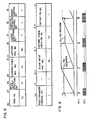
- Fig. 5 shows a task instruction specifying the following operation. That is, a task instruction stored in the k-th task register of the
task register group 103 specifies the input processing. The n1- th and ml-th registers of theregister group 105 are used as a counter/timer register and a capture register, respectively. The counter/timer register performs a counting operation for an external clock signal (p1) applied to the pith pin. When a capture signal (q1) applied to the ql-th pin takes a level "0", data held by the counter/timer register (namely, the n1-th register) is transferred to the capture register (namely, the m1-th register), and then the counter/timer register (namely, the nl-th register) is reset. In this case, the counter/timer operation part operates as shown in Fig. 6, in accordance with the task instruction. As is apparent from Fig. 6, the n1-th register (namely, the counter/timer register) is reset each time a trigger pulse (qi) from the qi-th pin is applied to the counter/timer register, and counts up the external clock pulses (p1) from the p1-th pin. - Further, the contents of the counter/timer register are transferred to the m1-th register (namely, the capture register) each time the trigger pulse is applied to the ql-th pin. It is to be noted that the contents of a register are given by analog representation in Figs. 6, 8, 10 and 12.
- Fig. 7 shows a task instruction specifying the following operation. That is, the counter/timer operation part performs an operation similar to the operation specified by the task instruction of Fig. 5, but a counter/timer register (namely, the n2-th register) continues a counting operation without being reset after data in the counter/timer register has been transferred to a capture register (namely, the m2-th register), since the 14th bit has a value "0". In this case, the counter/timer operation part operates as shown in Fig. 8, in accordance with the task instruction. That is, the contents of the n2-th register (namqly, the counter/ timer register) which counts up external clock pulses (P2) supplied from a pz-th pin, are transferred to the m2-th register (namely, the capture register) each time a trigger pulse (q2) from a q2-th pin is applied to the counter/timer register.
- Fig. 9 shows a task instruction for generating a constant interval or the like. Referring to Fig. 9, the task instruction is stored in the k3-th task register of the
task register group 103, and specifies the output processing since the 26th bit has a value "1". The n3-th register and the m3-th register of theregister group 105 are used as a counter/timer register and a compare register, respectively. - The counter/timer register performs a counting operation for an internal clock signal, since the clock specifying bit (namely, the 17th bit) has a value "0".
- Data in the counter/timer register is compared with data in the compare register. When the data in the counter/timer register coincides with or becomes greater than the data in the compare register, a logical value "0" is delivered to the 03- th pin and the counter/timer register is reset, since the logical value specifying bit (namely, the 12th bit) has a value "0" and the post-coincidence control bit (namely, the 13th bit) has a value "1". Fig. 10 shows the operation of the counter/timer operation part based upon the task instruction of Fig. 9. Referring to Fig. 10, when the contents of the n3-th register (namely, the counter/timer register) coincide with the contents of the m3-th register (namely, the compare register), an output pulse (03) is delivered to the 03-th pin and the n3-th register is reset.
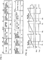
- Fig. 11 shows a task instruction forcontrolling a duty ratio. Referring to Fig. 11, the task instruction is stored in the k4-th task register of the
task register group 103, and specifies the output processing since the 26th bit has a value "1". The n4-th register and the m4-th register of theregister group 105 are used as a counter/timer register and a compare register, respectively, since the 25th to 22nd bits indicate the value "n4" and the 21st to 18th bits indicate the value "m4". - The counter/timer register performs a counting operation for an internal clock signal, since the 17th bit (namely, the clock specifying bit) has a value "0". The counter/timer register is reset by a reset pulse (q4) from the q4-th pin. Data in the counter/timer register is compared with data in the compare register. When the data in the counter/timer register coincides with or becomes greater than the data in the compare register, a logical value "0" is delivered to the o4-th pin, since the 12th pin (namely, the logical value specifying bit) has a value "0".
- Fig. 12 shows the operation of the counter/timer operation part based upon the task instruction of Fig. 11. It is to be noted that different reference data are written in the m4-th register (namely, the compare register) at time moments Wi, W2 and W3. The n4-th register (namely, the counter/timer register) counts up internal clock pulses (not shown). When the contents of the counter/timer register become greater than the contents of the compare register which has been loaded with the first reference data at the time moment W" at a time C" an output signal (04) supplied to the 04-th pin is put to a level "0". The counter/timer register continues to count up the internal clock pulses, but is reset when the reset pulse (q4) is applied to the q4-th pin, since the reset control bit (the 15th bit) of the task instruction is set to "1". Thus, the contents of the counter/timer register become smaller than those of the compare register, and hence the output signal (04) is returned to a level "1". Thereafter, the compare register is loaded with the second reference data which is greater than the first reference data, at the time moment W2. When the contents of the counter/timer register become equal to the second reference data at a time C2, the output signal (04) is put to the level "0". As is apparent from Fig. 12, the task instruction of Fig. 11 produces an output waveform having different duty ratios.
- When the task instructions of Figs. 5, 7, 9 and 11 are stored in the
task register group 103 of Fig. 2 and are successively scanned by the tasksignal generating circuit 101, the above-mentioned four counter/timer operations can be performed at once. - Referring back to Fig. 2, if an input/
output latch group 210 is connected to thedata bus 203 of the microcomputer, and an input/output pin selector 211 is provided for controlling the connection of thelatch group 210 with theoutput terminal group 209 and inputterminal group 208 by an instruction from the CPU, input/output pins which are not specified by task instructions to be executed, can be used as parallel I/O pins. - In each of the task instructions of Figs. 5, 7, 9 and 11, only two different registers of the
register group 105 are specified. However, the present invention is not limited to such task instructions, but a task instruction specifying three or more registers of theregister group 105 can also be used. - Further, in a case where it is required only to count up internal clock pulses by a counter/timer register, only a single register of the
register group 105 may be specified by a task instruction. - As is evident from the foregoing explanation, in a counter/timer device according to the present invention, different task instructions which are to be executed at once, can specify a single register of the register group in common. Moreover, the common register may be specified as a counter/ timer register in a task instruction and as a compare register in another task instruction. Accordingly, a counter/timer device according to the present invention can perform a more complicated counter/timer operation, as compared with a conventional counter/timer device.
- In short, according to the present invention, the number of counter/timer registers used in the input and output processing, the number of capture registers used in these processing and the number of compare registers used in the above processing are not fixed, but a counter/timer register, a capture register and a compare register can be freely selected from a register group by a simple instruction. Hence, a counter/timer device according to the present invention can be used for controlling various apparatuses.
- Further, according to the present invention, desired pins can be freely selected from an external pin group by a task instruction, and therefore the pin group can be used very effectively. Accordingly, a counter/timer device according to the present invention is advantageously incorporated in a single-chip microcomputer, in which the number of input/output pins is limited.
- When the clock signals CP1 and 03 do not utilize the memory cycle of the CPU but utilize the machine cycle, a single-chip microcomputer including a counter/timer device according to the present invention has a high processing speed, and exhibits an excellent performance.
- Further, according to the present invention, various functions in the input and output processing can be set by simple task instructions. That is, a counter/timer device according to the present invention has a high degree of freedom.
Claims (18)
Applications Claiming Priority (2)
| Application Number | Priority Date | Filing Date | Title |
|---|---|---|---|
| JP59230202A JPH06103507B2 (en) | 1984-11-02 | 1984-11-02 | Pulse input / output processor and microcomputer using the same |
| JP230202/84 | 1984-11-02 |
Publications (3)
| Publication Number | Publication Date |
|---|---|
| EP0180196A2 EP0180196A2 (en) | 1986-05-07 |
| EP0180196A3 EP0180196A3 (en) | 1988-04-06 |
| EP0180196B1 true EP0180196B1 (en) | 1990-01-31 |
Family
ID=16904176
Family Applications (1)
| Application Number | Title | Priority Date | Filing Date |
|---|---|---|---|
| EP85113745A Expired - Lifetime EP0180196B1 (en) | 1984-11-02 | 1985-10-29 | Programmable counter/timer device |
Country Status (5)
| Country | Link |
|---|---|
| US (1) | US4930100A (en) |
| EP (1) | EP0180196B1 (en) |
| JP (1) | JPH06103507B2 (en) |
| KR (1) | KR920008070B1 (en) |
| DE (1) | DE3575797D1 (en) |
Families Citing this family (25)
| Publication number | Priority date | Publication date | Assignee | Title |
|---|---|---|---|---|
| US5081297A (en) * | 1986-05-06 | 1992-01-14 | Grumman Aerospace Corporation | Software reconfigurable instrument with programmable counter modules reconfigurable as a counter/timer, function generator and digitizer |
| JPS63118948A (en) * | 1986-11-07 | 1988-05-23 | Nec Corp | Single chip microcomputer |
| JPH0210417A (en) * | 1988-06-28 | 1990-01-16 | Fujitsu Ltd | Counter circuit |
| JP2725205B2 (en) * | 1988-07-08 | 1998-03-11 | シーメンス、アクチエンゲゼルシヤフト | Microcontroller counter / timer circuit |
| US4926319A (en) * | 1988-08-19 | 1990-05-15 | Motorola Inc. | Integrated circuit timer with multiple channels and dedicated service processor |
| US4942522A (en) * | 1988-08-19 | 1990-07-17 | Motorola, Inc. | Timer channel with multiple timer reference features |
| US5042005A (en) * | 1988-08-19 | 1991-08-20 | Motorola, Inc. | Timer channel with match recognition features |
| US4952367A (en) * | 1988-08-19 | 1990-08-28 | Motorola, Inc. | Timer channel for use in a multiple channel timer system |
| US5175699A (en) * | 1988-10-28 | 1992-12-29 | Dallas Semiconductor Corp. | Low-power clock/calendar architecture |
| US5418932A (en) * | 1990-02-01 | 1995-05-23 | Hitachi, Ltd. | Generation of width modulated pulses by relatively adjusting rising and falling edges upon comparison of counter with programmably stored values |
| JP2669158B2 (en) * | 1991-01-22 | 1997-10-27 | 三菱電機株式会社 | Data processing device |
| US5333295A (en) * | 1991-04-11 | 1994-07-26 | Dallas Semiconductor Corp. | Memory control system |
| US5678019A (en) * | 1993-02-05 | 1997-10-14 | Dallas Semiconductor Corporation | Real-time clock with extendable memory |
| US5471608A (en) * | 1993-12-09 | 1995-11-28 | Pitney Bowes Inc. | Dynamically programmable timer-counter having enable mode for timer data load and monitoring circuit to allow enable mode only upon time-out |
| US5475621A (en) * | 1993-12-09 | 1995-12-12 | Pitney Bowes Inc. | Dual mode timer-counter |
| US5729721A (en) * | 1995-11-13 | 1998-03-17 | Motorola, Inc. | Timebase synchronization in separate integrated circuits or separate modules |
| US5812833A (en) * | 1995-11-13 | 1998-09-22 | Motorola, Inc. | Timer bus structure for an integrated circuit |
| US5701421A (en) * | 1995-11-13 | 1997-12-23 | Motorola, Inc. | Pin and status bus structure for an integrated circuit |
| US5631853A (en) * | 1995-11-13 | 1997-05-20 | Motorola Inc. | Flexible configuration of timebases in a timer system |
| US5634045A (en) * | 1995-11-13 | 1997-05-27 | Motorola, Inc. | Integrated circuit input/output processor having improved timer capability |
| US5732225A (en) * | 1995-11-13 | 1998-03-24 | Motorola Inc. | Integrated circuit timer system having a global bus for transferring information between local buses |
| US5721888A (en) * | 1995-11-13 | 1998-02-24 | Motorola, Inc. | Performing flexible logical operations with timer channel outputs |
| US5721889A (en) * | 1995-11-13 | 1998-02-24 | Motorola, Inc. | Data transfer between integrated circuit timer channels |
| US6002285A (en) * | 1996-05-28 | 1999-12-14 | International Business Machines Corporation | Circuitry and method for latching information |
| US6802362B2 (en) * | 2002-02-21 | 2004-10-12 | Thermal Corp. | Fin with elongated hole and heat pipe with elongated cross section |
Family Cites Families (10)
| Publication number | Priority date | Publication date | Assignee | Title |
|---|---|---|---|---|
| US4348743A (en) * | 1976-09-27 | 1982-09-07 | Mostek Corporation | Single chip MOS/LSI microcomputer with binary timer |
| GB2014764B (en) * | 1978-02-17 | 1982-09-15 | Casio Computer Co Ltd | Time data processing apparatus |
| JPS551556A (en) * | 1978-06-20 | 1980-01-08 | Seiko Instr & Electronics Ltd | Multifunctional electronic watch |
| US4222103A (en) * | 1978-09-25 | 1980-09-09 | Motorola, Inc. | Real time capture registers for data processor |
| JPS5595892A (en) * | 1979-01-17 | 1980-07-21 | Hitachi Ltd | Electronic digital multi-function watch |
| US4245323A (en) * | 1979-01-26 | 1981-01-13 | Copal Co., Ltd. | Electronic calculator with time display function |
| JPS5890404U (en) * | 1981-12-07 | 1983-06-18 | 株式会社明電舎 | Timer/counter circuit |
| JPS58182326A (en) * | 1982-04-19 | 1983-10-25 | Matsushita Electric Ind Co Ltd | Program memory device |
| US4538235A (en) * | 1982-08-19 | 1985-08-27 | Rockwell International Corporation | Microcomputer retriggerable interval counter |
| US4618968A (en) * | 1983-11-04 | 1986-10-21 | Motorola, Inc. | Output compare system and method automatically controlilng multiple outputs in a data processor |
-
1984
- 1984-11-02 JP JP59230202A patent/JPH06103507B2/en not_active Expired - Lifetime
-
1985
- 1985-10-29 DE DE8585113745T patent/DE3575797D1/en not_active Expired - Lifetime
- 1985-10-29 EP EP85113745A patent/EP0180196B1/en not_active Expired - Lifetime
- 1985-10-30 KR KR1019850008026A patent/KR920008070B1/en not_active IP Right Cessation
-
1988
- 1988-12-14 US US07/284,388 patent/US4930100A/en not_active Expired - Lifetime
Also Published As
| Publication number | Publication date |
|---|---|
| JPS61110254A (en) | 1986-05-28 |
| EP0180196A3 (en) | 1988-04-06 |
| US4930100A (en) | 1990-05-29 |
| DE3575797D1 (en) | 1990-03-08 |
| JPH06103507B2 (en) | 1994-12-14 |
| KR920008070B1 (en) | 1992-09-22 |
| EP0180196A2 (en) | 1986-05-07 |
| KR860004352A (en) | 1986-06-20 |
Similar Documents
| Publication | Publication Date | Title |
|---|---|---|
| EP0180196B1 (en) | Programmable counter/timer device | |
| US4591979A (en) | Data-flow-type digital processing apparatus | |
| US4672534A (en) | Integrated circuit device incorporating a data processing unit and a ROM storing applications program therein | |
| US5511207A (en) | Program control circuit determining the designated number of times a sequence of instructions is repetitively executed to prevent further execution of a jump instruction | |
| US4870562A (en) | Microcomputer capable of accessing internal memory at a desired variable access time | |
| US5136662A (en) | Image processor for sequential processing of successive regions of an image | |
| US4785416A (en) | Microprocessor timing emulator having a "Wait" state | |
| EP0291581A2 (en) | Logic integrated circuit capable of simplifying a test | |
| US4670879A (en) | Pattern generator | |
| US4584642A (en) | Logic simulation apparatus | |
| US5089955A (en) | Programmable counter/timer device with programmable registers having programmable functions | |
| US4435757A (en) | Clock control for digital computer | |
| US5497459A (en) | System for testing instruction queue circuit and central processing unit having the system | |
| EP0377976B1 (en) | Microcode control apparatus utilizing programmable logic array circuits | |
| US5261116A (en) | Programmable, expandable controller with flexible I/O | |
| US5079694A (en) | Data processing apparatus having a working memory area | |
| US5526500A (en) | System for operand bypassing to allow a one and one-half cycle cache memory access time for sequential load and branch instructions | |
| US5872961A (en) | Microcomputer allowing external monitoring of internal resources | |
| US4408276A (en) | Read-out control system for a control storage device | |
| US4888685A (en) | Data conflict prevention for processor with input/output device | |
| US5179716A (en) | Programmable expandable controller with flexible I/O | |
| US5050076A (en) | Prefetching queue control system | |
| EP0020972A1 (en) | Program controlled microprocessing apparatus | |
| JPS6410854B2 (en) | ||
| US5826063A (en) | Apparatus and method for programming the setup, command and recovery time periods within a transaction cycle |
Legal Events
| Date | Code | Title | Description |
|---|---|---|---|
| PUAI | Public reference made under article 153(3) epc to a published international application that has entered the european phase |
Free format text: ORIGINAL CODE: 0009012 |
|
| AK | Designated contracting states |
Kind code of ref document: A2 Designated state(s): DE FR GB IT |
|
| PUAL | Search report despatched |
Free format text: ORIGINAL CODE: 0009013 |
|
| AK | Designated contracting states |
Kind code of ref document: A3 Designated state(s): DE FR GB IT |
|
| 17P | Request for examination filed |
Effective date: 19880408 |
|
| 17Q | First examination report despatched |
Effective date: 19890502 |
|
| GRAA | (expected) grant |
Free format text: ORIGINAL CODE: 0009210 |
|
| AK | Designated contracting states |
Kind code of ref document: B1 Designated state(s): DE FR GB IT |
|
| REF | Corresponds to: |
Ref document number: 3575797 Country of ref document: DE Date of ref document: 19900308 |
|
| ET | Fr: translation filed | ||
| ITF | It: translation for a ep patent filed |
Owner name: MODIANO & ASSOCIATI S.R.L. |
|
| PLBE | No opposition filed within time limit |
Free format text: ORIGINAL CODE: 0009261 |
|
| STAA | Information on the status of an ep patent application or granted ep patent |
Free format text: STATUS: NO OPPOSITION FILED WITHIN TIME LIMIT |
|
| 26N | No opposition filed | ||
| ITTA | It: last paid annual fee | ||
| PGFP | Annual fee paid to national office [announced via postgrant information from national office to epo] |
Ref country code: FR Payment date: 19980915 Year of fee payment: 14 |
|
| PGFP | Annual fee paid to national office [announced via postgrant information from national office to epo] |
Ref country code: GB Payment date: 19980930 Year of fee payment: 14 |
|
| PGFP | Annual fee paid to national office [announced via postgrant information from national office to epo] |
Ref country code: DE Payment date: 19981231 Year of fee payment: 14 |
|
| PG25 | Lapsed in a contracting state [announced via postgrant information from national office to epo] |
Ref country code: GB Free format text: LAPSE BECAUSE OF NON-PAYMENT OF DUE FEES Effective date: 19991029 |
|
| GBPC | Gb: european patent ceased through non-payment of renewal fee |
Effective date: 19991029 |
|
| PG25 | Lapsed in a contracting state [announced via postgrant information from national office to epo] |
Ref country code: FR Free format text: LAPSE BECAUSE OF NON-PAYMENT OF DUE FEES Effective date: 20000630 |
|
| PG25 | Lapsed in a contracting state [announced via postgrant information from national office to epo] |
Ref country code: DE Free format text: LAPSE BECAUSE OF NON-PAYMENT OF DUE FEES Effective date: 20000801 |
|
| REG | Reference to a national code |
Ref country code: FR Ref legal event code: ST |