EP0177848A2 - LSI microprocessor chip with backward pin compatibility and forward expandable functionality - Google Patents
LSI microprocessor chip with backward pin compatibility and forward expandable functionality Download PDFInfo
- Publication number
- EP0177848A2 EP0177848A2 EP85112234A EP85112234A EP0177848A2 EP 0177848 A2 EP0177848 A2 EP 0177848A2 EP 85112234 A EP85112234 A EP 85112234A EP 85112234 A EP85112234 A EP 85112234A EP 0177848 A2 EP0177848 A2 EP 0177848A2
- Authority
- EP
- European Patent Office
- Prior art keywords
- chip
- pins
- functionality
- unused
- functional
- Prior art date
- Legal status (The legal status is an assumption and is not a legal conclusion. Google has not performed a legal analysis and makes no representation as to the accuracy of the status listed.)
- Withdrawn
Links
Images


Classifications
-
- G—PHYSICS
- G06—COMPUTING OR CALCULATING; COUNTING
- G06F—ELECTRIC DIGITAL DATA PROCESSING
- G06F15/00—Digital computers in general; Data processing equipment in general
- G06F15/76—Architectures of general purpose stored program computers
- G06F15/78—Architectures of general purpose stored program computers comprising a single central processing unit
- G06F15/7839—Architectures of general purpose stored program computers comprising a single central processing unit with memory
- G06F15/7842—Architectures of general purpose stored program computers comprising a single central processing unit with memory on one IC chip (single chip microcontrollers)
-
- G—PHYSICS
- G06—COMPUTING OR CALCULATING; COUNTING
- G06F—ELECTRIC DIGITAL DATA PROCESSING
- G06F1/00—Details not covered by groups G06F3/00 - G06F13/00 and G06F21/00
- G06F1/22—Means for limiting or controlling the pin/gate ratio
-
- G—PHYSICS
- G06—COMPUTING OR CALCULATING; COUNTING
- G06F—ELECTRIC DIGITAL DATA PROCESSING
- G06F12/00—Accessing, addressing or allocating within memory systems or architectures
- G06F12/02—Addressing or allocation; Relocation
- G06F12/06—Addressing a physical block of locations, e.g. base addressing, module addressing, memory dedication
- G06F12/0615—Address space extension
- G06F12/0623—Address space extension for memory modules
Definitions
- This invention relates to data processing and more particularly to microprocessor chips.
- compatibility in such instances has been achieved by emulation through microprogramming, by modifying portions of the operating system, or by utilizing similar architectures. While such compatibility has been achieved, these chips are still able to provide only a downward software compatibility. This means that the same software written for 8- or 16-bit microprocessor chips can be executed on 32-bit chips.
- the above and other objects are achieved in a preferred embodiment of a microprocessor chip which incorporates the apparatus and methodology of the present invention.
- the chip implemented in large scale integration (LSI) using advanced techniques is designed to include a number of compatibility circuits which connect to a corresponding number of pins which corresponds to unused pins of the chip it is to replace in an existing computer system.
- Each compatibility circuit connects to those internal parts of the new LSI chip that have newly added or altered functionality.
- the compatibility circuits inhibit the operation of the added/altered functionality.
- these circuits condition other parts of the chip, in addition to the added functionality to the extent required to operate in the same manner as the replaced chip, but with the higher speed and improved performance attainable by the use of new technology.
- an external circuit is connected to the compatibility circuit which permits the chip to operate with the desired expanded level functionality at the same higher speed and improved performance.
- each of the compatibility circuits are connected to be clocked by timing signals generated within the system so as to reduce to a minimum the number of unused pins required for the different levels of functionality.
- the new LSI microprocessor chip employs more advanced solid state techniques (new technology) in its construction. This resulted in superior speed, improved performance, lower power consumption and simpler fabrication as compared to the prior LSI microprocessor chip. Additionally, the new chip incorporates expandable new functionality which is reflected in an enhanced addressing capability. This is reflected in the assignment of additional pins for other address bits. The additional pins correspond to unused pins of the chip being replaced. Thus, the new chip has complete hardware downward compatibility with the old chip. That is, the new chip has backward pin compatibility with the old chip.
- the chip of the present invention can be used in two distinct systems (i.e., new and existing system designs) without having to make any changes in the design of such systems.
- inventory and maintenance requirements are reduced significantly.
- the need to retrofit existing systems to utilize the new chip has been eliminated.
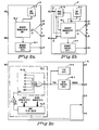
- Figures la and lb show in pictorial form the input and output pin connections of the microprocessors fabricated on single integrated circuit substrates or chips. As shown, each chip has 68 pins, several of which have no connections within the minicomputer system in which they are used. These pins are designated as spares in Figures la and lb.
- Each of the chips 10 and 12 have a number of unshared pins as for example pins 1, 14, 16, 17, 31 and 65. These pins are connected to receive supply voltages, clocking signals, timer and clear signals, as shown.
- a second group of pins of both chips 10 and 12 connect to the address and data interface lines of the microprocessor bus.
- the group includes ROS address bus pins 40 through 51 and the address/data bus pins 6 through 29.
- LSI chip 12 also has pins 3, 2 and 68 connected to the address interface lines while pins 3, 2 and 68 of chip 10 remain unconnected in its system.
- a third group of pins of chips 10 and 12 connect to the monitor/interrupt and memory management unit (MMU) circuits.
- the group includes data request pins 32 through 36, major branch test group pins 59 through 62, interrupt request pins 04, 67 and 66, control input pins 56 through 63 and memory control input pins 30, 37 and 36, in addition to a memory error violation output pin 34.
- pins 2, 3 and 68 of chip 10 are unconnected in its system, while these same pins in chip 12 are connected in its system.
- Each of the pins 2, 3 and 68 of chip 12 is connected to receive a signal which defines in which system the chip is being used (i.e., its application in an existing or new minicomputer system) .
- pins 2, 3 and 68 are unconnected as in chip 10.
- either pin 2, 3 or 68 is connected to an externally applied reference input signal which will be activated during chip control input time.
- pins 2, 3 and 68 are connected to provide levels of additional or expanded functionality as explained herein during chip system output time.
- FIGs 2a, 2c and 2b, 2d illustrate in part the organizations of chips 10 and 12.
- the microprocessor of chip 10 is organized to be functionally equivalent to the central processing unit described in U.S. Patent No. 4,340,933 which issued July 20, 1982 and is assigned to the same assignee as named herein.
- chip 10 includes a memory management unit MMU 10-2, the memory control circuits of block 10-4 and interrupt processing circuits of block 10-6.
- MMU 10-2 includes a 12-bit adder 10-20 and the error circuits of block 10-24.
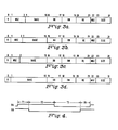
- MMU 10-2 operates to translate 20-bit memory virtual (logical) addresses into 20-bit physical addresses utilizing segment descriptors having the format of Figure 3a.
- bit 0 is a validity bit.
- an OR circuit of block 10-24 signals that the segment is undefined or invalid by forcing an unavailable resource signal T15E to a ONE.
- the fields containing bits 1-3 and bits 22 must be all ZEROS or the MMU 10-2 signals that the segment is undefined. That is, this check is performed by OR circuit of block 10-24 forcing signal T15E to a ONE when any one of the bits Al, A2, A3 or A22 is a ONE.
- Bits 4-15 constitute a 12-bit segment base which the MMU adder 10-20 adds to an 8-bit block number field (BIO-7) of the virtual or logical address, the sum of which is applied to output address/data bus of chip 10.
- BIO-7 block number field
- the logical address on the internal bus consists of 20 bits formatted, as shown below.
- Bits 16-21 are three 2-bit ring protection fields which define memory access rights (i.e., RR-read, RW-write and R E-execute). Since these fields are not pertinent to an understanding of the present invention, they are not discussed herein.
- bits 23-31 are a 9-bit size field for the memory segment associated with the segment descriptor.
- MMU 10-2 compares the size field to the 9-bit block number field to verify that the descriptor size field is equal to or greater than the binary value of the bits contained in the block number field of the logical address. As discussed herein, this size check verifies that the block number of the logical address does not exceed the assigned number of blocks specified in the segment descriptor. When this condition is not met, signal CMP is forced to a ONE. This check is performed by OR circuit of block 10-24 forcing signal T15E to a ONE when signal CMP is a ONE. This ensures that normal access is to an available area of memory. For further details about how such checking may be accomplished, reference may be made to U. S. Patent No. 4,378,591 issued March 29, 1983 which is assigned to the same assignee as named herein.
- MMU 10-2 performs the number of checks indicated, and generates appropriate error signals, such as signal T15E indicating whether or not memory access is legal or valid.
- the error signal T15E is stored one of several control flip-flops (not shown) included in MMU 10-2.
- the output from this control flip-flop is applied by MMU 10-2 as appropriate trap vector signals to the interrupt processing circuits of block 10-6.
- the trap vector signals are processed in the manner described in U.S. Patent No. 4,074,353, issued February 14, 1978, and is assigned to the same assignee as named herein.
- the same error signal T15E generated by MMU 10-2 is applied to the memory control circuits of block 10-4.
- These circuits in turn apply an output signal MEMKIL to pin 34 of chip 10 which is used to prevent the alteration of information stored in the memory units within the system when MMU 10-2 has detected an illegal access.
- Microprocessor chip 12 is organized to have a number of levels of expanded and new functionality in contrast to that of the chip 10 microprocessor.
- MMU 12-2 includes a 15-bit adder 12-20 and the error circuits of block 12-24.
- MMU 12-2 operates to translate 20-bit virtual memory addresses into 20-bit, 21-bit, 22-bit or 23-bit physical addresses utilizing the descriptors formatted as shown in Figures 3a through 3d, respectively.
- MMU adder 12-20 adds the 12-bit, 13-bit, 14-bit or 15-bit base address field of the segment descriptor to a 9-bit block number derived from the logical address applied to the chip's internal bus.
- An unchanged offset field of the logical address is appended to the 12-bit, 13-bit, 14-bit or 15-bit sum applied to chip pins 29 through 18 and 3, 2 or 68 to create the 20-bit, 21-bit, 22-bit or 23-bit physical address.
- chip 12 includes the plurality of compatibility circuits 12-10A, 12-10B and 12-10C of block 12-10, the memory control circuits of block 12-4 and interrupt circuits of block 12-6.
- Each of the compatibility circuits 12-10A, 12-10B and 12-10C of block 12-10 connect to pins 3, 2 and 68, respectively. As explained herein, they condition the remaining circuits of MMU 12-2 of chip 12 to operate within either of two systems. That is, the circuits 12-10A, 12-10B and 12-10C of block 12-10 provide the appropriate signals for conditioning the error circuits of block 12-24 and adder 12-20 to operate in either system.
- error circuits of block 12-24 have been modified from the circuits of block 10-24.
- the OR circuit of block 12-24 essentially has the same number of inputs as the OR circuit of block 10-24.
- the reason, as explained in detail herein, is that the thirteenth, fourteenth and fifteenth stages (new functionality) are implemented to generate signals which produce the correct error responses for either system.
- the signals for either system are established by the compatibility circuits 12-10A, 12-10B and 12-10C of block 12-10.
- address bits A3, A2 and Al are no longer inputs to the circuits of block 12-24 (no longer part of the must be zero (MBZ) check). That is, each of the address bits A3, A2 and Al are inputs to a different one of the expanded last stages of adder 12-20, as shown. Also, the circuits of block 12-24 receive the carry out signal CYOUT from these adder stages instead of carry out signal CY3. Lastly, the circuits of block 12-24 receive the sum bits which correspond to signals MM21, MM22 and MM23 produced by the adder stages as a function which system, chip 12 is operating and the level of functionality selected as defined by the compatibility circuits 12-10A, 12-10B and 12-10C of block 12-10.
- each of the compatibility circuits 12-10A, 12-10B and 12-10C connect to a different one of the pins 3, 2 and 64, respectively, as shown.
- Each circuit includes a transparent latch (i.e., 12-102A, 12-102B and 12-102C) and a resistor to voltage +V (12-100A, 12-100B and 12-100C).
- Each latch is clocked by the combination of phase A and phase B, timing signals OA and OB received from the system clock, not shown,.
- phase A and phase B timing signals are high (ONES)
- the state of the pin to which it connects is going to be clocked into the latch. That is, latch E, F and G will store that fact of whether or not pins 3, 2 and 64, respectively, were activated low.
- the driver circuit includes an inverting tristate buffer circuit 14-15, such as part number 74S240 manufactured by Texas Instruments Inc.
- the driver input connects to a voltage +V through a pull up resistor 14-10.
- the binary 1 output latch EL connects to one input of an AND gate 12-240 of block 12-24.
- Latch F connects as one input of AND gates 12-240, 12-242 and 12-244.
- Latch G connects to one input of AND gates 12-240, 12-242, 12-244, 12-246 and 12-248, as shown.
- the AND gates 12-240, 12-244 and 12-248 receive inputs from the sum outputs (E, F and G) of adder stages 13, 14 and 15, respectively.
- the AND gates 12-242 and 12-246 receive the carry output (COE, COF) from the thirteenth and fourteenth adder stages, respectively.
- Each of the adder stages includes an exclusive OR gate (i.e., 12-202, 12-206, 12-210) and an AND gate (i.e., 12-204, 12-208, 12-212).
- the sum output (E, F, G) of each adder stage is applied via a tristate output buffer stage (i.e., 12-200, 12-201, 12-203) to one of the previously unused pins 3, 2 and 68 to which its corresponding transparent latch connects.
- each exclusive OR circuit i.e., 12-202, 12-206 and adder stage 12-210
- each exclusive OR circuit generates a binary ONE for its expanded address bit (i.e., MM21, MM22, MM23) when the input address bit (i.e., A3,. A2, -Al) is a binary ONE and the carry in from the previous stage is a binary ZERO.
- the same output is generated when the input address bit is a binary ZERO and the carry in from the previous stage (i.e., COD, COE, COF) is a binary ONE.
- Each adder stage AND gate (i.e., 12-204, 12-208 and 12-212) generates a binary ONE carry out signal (i.e., COE, COF, COG) when both its input address bit (i.e., A3, A2, Al) and the carry in from the previous stage (i.e., COD, COE, COF) are binary ONES.
- both the expanded address bit signals i.e., E, F, G
- carry out signals i.e., COE, COF, COG
- carry out signal COG of adder stage 15 is an ungated input to these circuits (i.e., directly connected).
- the error circuits further include an OR gate 12-250.
- the OR gate 12-250 ensures error signal T15E is generated when any one of the same A0, A22 and CMP is forced to a binary ONE.
- each of the transparent latches 12-102A, 12-102B and 12-102C is implemented by a standard configuration which includes a pair of series connected MOSFET inverters and MOSFET transistors.
- As an input signal is applied to a first MOSFET transistor gated by timing signals OA ⁇ OB (i.e., time Tl).
- the output of the transistor is applied to the input of the first inverter while the output of the second inverter is recirculated back to the input of the first transistor through a second MOSFET transistor which is gated by timing signals OA ⁇ OB (i.e., time Tl ).
- chip 12 is constructed from a more advanced technology than chip 10. That is, chip 12 was developed using a process which takes advantage of smaller geometries resulting in faster circuits and improved performance. More importantly, the smaller geometries provide higher yields resulting in reduced costs in manufacturing chip 12.
- chip 12 has been installed into an existing system which was designed to utilize chip 10 (hereinafter old system).
- pins 2, 3 and 68 of chip 12 of Figure 2d are unconnected. Therefore, the signals applied to compatibility circuit latches E, F and G of blocks 12-10A, 12-10B and 12-10C are at approximately voltage V representative of a binary ONE.
- signal T15E will change state as a function of address bits 13, 14 and 15 (i.e., MM21, MM22, MM23) which correspond to the sums of segment descriptor bits 3 (A3), 2 (A2), 1 (Al) and the carry out (CY3/COD) , (COE), (COF) and (COG) from adder stages twelve, thirteen, fourteen and fifteen.
- phase A signal OA is used by chip 12 and the system in which chip 12 is included to reverse the direction of the I/O drivers.
- phase A signal OA is a binary ONE
- the ROS data lines and option lines are inputs to chip 12.
- phase A signal OA is a binary ZERO, all other shared signals are either inputs or outputs to chip 12.
- Phase B signal OB is used to latch the signals that were gated with phase A signal OA.
- phase B signal OB goes to a binary ZERO, the ROS data and options are latched internally within chip 12.
- phase B signal OB goes to a binary ONE, all other shared signals are latched internally.
- phase A and B signals OA and OB are divided into time intervals Tl through T4.
- the firmware control word is being loaded into chip 12. This sets up the cycle which is going to occur.
- the MMU MOSFET circuits are precharged while the logical address which will be applied to the internal bus for accessing the correct segment descriptor is being established.
- the signals OA and OB which define time Tl, are applied to each of the transparent latches 12-102A, 12-102B and 12-102C. This enables the states of the corresponding pins to be sampled at the same time the firmware control word is being loaded into chip 12.
- external driver circuit 14-15 operates to force output signal DABSOX+XX active low or a binary ZERO. If connected, this causes one of the signals DABSOE+EE, DABSOF+EF or DABSOG+EG to be active low.
- the outputs of adder stages 13, 14 and 15 are applied to pins 3, 2 and 68, respectively.
- chip 12 is connected to provide a first level of functionality wherein the MMU address capability is expanded or extended by one address bit, so that it now has 21 bits of addressing, as shown, in Figure 3b.
- external driver circuit 14-15 is wired to pin 3 of chip 12 which applies signal DABSOE+EE to that pin. The remaining unused pins 2 and 68 remain unconnected.
- pin 3 will now be time shared.
- external driver circuit 14-15 is enabled to drive pin 3 to a predetermined state (i.e., active low), treating it as if it were a control bit or any option bit. In this case, it can be viewed as a special type of option bit.
- a binary ZERO signal is latched into latch 12-102A at time Tl.
- binary ONES are latched into latches 12-102B and 12-102C, since there is nothing tied to pins 2 and 68. That is, the voltage +V is applied to the inputs of both latches.
- all of the address conditions are examined.
- the output EL of latch E is low (i.e., a binary ZERO) while the outputs FL and GL of latches F and G are high (i.e., binary ONES).
- adder stage 13 is permitted to generate address bit 21 (i.e., signal MM21) without producing an error condition. That is, the binary ZERO state of signal EL inhibits AND gate 12-240 from forcing error signal T15E to a binary ONE.
- the generated address signal MM21 is applied to pin 3 via tristate buffer circuit 12-200 during system time.
- address bit 22 or 23 i.e., signals MM22, MM23
- adder stage 14 or 15 also produces an error. That is, when address bit 22 (MM22) is forced to a binary ONE, AND gate 12-244 is conditioned by the binary ONE states of latch output signals FL and GL to force error signal T15E to a binary ONE. Similarly, when address bit 23 (MM23) is forced to a binary ONE, AND gate 12-248 is conditioned by the binary ONE state of latch output signal GL to force error signal T15E to a binary ONE. Also, the generation of a carry out from either adder stage 14 or 15 also produces an error.
- pins 2 and 3 will be time shared. Again, as previously described, external driver circuit 14-15 is enabled to drive pin 2 active low. When signal DABSOF+EF is' driven active. low, a binary ZERO signal is latched into latch 12-102B at time Tl. Simultaneously, binary ONES are latched into latches 12-102A and 12-102C, since there is nothing tied to pins 3 and 68 during phase A high time.
- the output FL of latch F is low (i.e., a binary ZERO), while outputs EL and GL of latches E and G are high (i.e., binary ONES).
- address bit 21 the binary ZERO output from latch F inhibits AND gate 12-240 from generating an error signal.
- adder stage 13 generates carry out signal COE. That is, latch F when a binary ZERO inhibits AND gate 12-242 from generating an error signal.
- address bit 22 the latch F binary ZERO inhibits AND gate 12-244 from generating an error signal.
- the generated Address bitsignals in MH21 and MM22 are applied to pins 3 and 2, respectively, via tristate buffer circuits 12-200 and 12-201 during system time.
- AND gate 12-246 conditioned by the binary ONE output from latch G, forces trap error signal T15E to a binary ONE.
- chip 12 is connected to provide a third level of functionality, wherein the MMU address capability is expanded by three address bits, so that it now has 23 bits of addressing as illustrated by Figure 3d.
- external driver circuit 14-15 is wired to pin 68 of chip 12 which applies signal DABSOG+EG to that pin.
- the other unused pins 3 and 2 remain unconnected to external tristate driver circuit 14-15.
- pins 3, 2 and 68 will now be time shared.
- external driver circuit 14-15 drives pin 68 active low.
- signal DABSOG+EG is driven active low, a binary ZERO signal is latched into latch 12-102C at time Tl.
- binary ONES are latched into latches 12-102A and 12-102B, since there is nothing tied to pins 3 and 2 during phase A high time.
- the binary ZERO from latch G inhibits AND gates 12-240, 12-242, 12-244, 12-246 and 12-248. That is, it inhibits the generation of an error signal when any one of the address bits 21, 22 or 23 is a ONE or there is a carry out from adder stage 13 or 14. However, a carry out from adder stage 15 is allowed to cause an error.
- the same chip is backward compatible with older systems which require no connections of the unused pins. That is, the present invention enables chip 12 to operate within at least two systems having different functionality.
- the invention makes it possible to utilize chips developed with new technology at lower cost to be utilized in older systems without requiring any changes to be made to such systems.
- the invention permits the older systems to operate with newer chips with the attendant speed and cost advantages and no change to system functionality or operation.
Landscapes
- Engineering & Computer Science (AREA)
- Theoretical Computer Science (AREA)
- Physics & Mathematics (AREA)
- General Engineering & Computer Science (AREA)
- General Physics & Mathematics (AREA)
- Computer Hardware Design (AREA)
- Microcomputers (AREA)
- Semiconductor Integrated Circuits (AREA)
- Design And Manufacture Of Integrated Circuits (AREA)
Abstract
Description
- Copending patent application of Eugene Nusinov and John J. Bradley, titled "LSI Microprocessor Chip with Backward Pin Compatibility", Serial Number 06/596,756, filed on April 4, 1984, and assigned to the same assignee as named herein.
- This invention relates to data processing and more particularly to microprocessor chips.
- With the significant and rapid changes in technology, manufacturers of minicomputer systems find it necessary to upgrade their systems more frequently than before. The upgrading process has taken the form of introducing new systems of retrofiting of old systems or a combination of both.
- The introduction of new microprocessor chip designs has been a significant driving force in computer system upgrading. Constantly, chip manufacturers are designing new chips that offer increased functionality and higher speeds. These new faster chips are in turn being made the basis of new system designs.
- The chip manufacturers and computer system manufacturers have recognized and continue to recognize the importance of compatibility between microprocessors. For example, several manufacturers of 32-bit microprocessors introduced in 1983 have emphasized their capability to run software written for microprocessors that had preceded them.
- For the most part, compatibility in such instances .has been achieved by emulation through microprogramming, by modifying portions of the operating system, or by utilizing similar architectures. While such compatibility has been achieved, these chips are still able to provide only a downward software compatibility. This means that the same software written for 8- or 16-bit microprocessor chips can be executed on 32-bit chips.
- However, as chip designs continue to evolve minicomputer manufacturers still will be required to maintain inventories of those different microprocessor chips utilized in new and old minicomputer designs. That is, downward software compatibility does not require downward hardware compatibility.
- In fact, the opposite is usually the case. This means that in order for an older minicomputer system to take advantage of a new chip, it is necessary to redesign or retrofit the system to accept the new chip notwithstanding the compatibilities in chip pin assignments. The reason is that the new chip besides being faster usually includes new functionality which enhances it marketability. This can prove costly in terms of both equipment maintenance and inventory.
- Accordingly, it is a primary object of the present invention to provide an improved design methodology and apparatus for providing compatibility in chip designs.
- It is a more specific object of the present invention to provide a chip which is usable in both new and older systems without requiring changes to be made to such older systems.
- The above and other objects are achieved in a preferred embodiment of a microprocessor chip which incorporates the apparatus and methodology of the present invention. The chip implemented in large scale integration (LSI) using advanced techniques is designed to include a number of compatibility circuits which connect to a corresponding number of pins which corresponds to unused pins of the chip it is to replace in an existing computer system. Each compatibility circuit connects to those internal parts of the new LSI chip that have newly added or altered functionality. When the new LSI chip is plugged into the existing minicomputer system, the compatibility circuits inhibit the operation of the added/altered functionality. At the same time, these circuits condition other parts of the chip, in addition to the added functionality to the extent required to operate in the same manner as the replaced chip, but with the higher speed and improved performance attainable by the use of new technology. When the new chip is placed in the system for which it was designed, an external circuit is connected to the compatibility circuit which permits the chip to operate with the desired expanded level functionality at the same higher speed and improved performance. Additionally, each of the compatibility circuits are connected to be clocked by timing signals generated within the system so as to reduce to a minimum the number of unused pins required for the different levels of functionality.
- More particularly, in the preferred embodiment, the new LSI microprocessor chip employs more advanced solid state techniques (new technology) in its construction. This resulted in superior speed, improved performance, lower power consumption and simpler fabrication as compared to the prior LSI microprocessor chip. Additionally, the new chip incorporates expandable new functionality which is reflected in an enhanced addressing capability. This is reflected in the assignment of additional pins for other address bits. The additional pins correspond to unused pins of the chip being replaced. Thus, the new chip has complete hardware downward compatibility with the old chip. That is, the new chip has backward pin compatibility with the old chip.
- Because of the above built in backward pin compatibility, the chip of the present invention can be used in two distinct systems (i.e., new and existing system designs) without having to make any changes in the design of such systems. Thus, inventory and maintenance requirements are reduced significantly. Also, the need to retrofit existing systems to utilize the new chip has been eliminated.
- The novel features which are believed to be characteristic of the invention both as to its organization and method operation, together with further objects and advantages will be better understood from the following description when considered in connection with the accompanying drawings. It is to be expressly understood, however, that each of the drawings are given for the purpose of illustration and description only and are not intended as a definition of the limits of the present invention.
-
- Figures la and lb are pictorial representations of chips used to illustrate the principles of the present invention.
- Figures 2a, 2c and 2b, 2d, respectively, show in block diagram form, portions of the microprocessor chips of Figures la and lb.
- Figures 3a through 3d show the formats of segment descriptors processed by the chips of Figures 2a and 2b.
- Figure 4 shows the timing portions of the chip of Figure 2b constructed according to the principles of the present invention.
- Figures la and lb show in pictorial form the input and output pin connections of the microprocessors fabricated on single integrated circuit substrates or chips. As shown, each chip has 68 pins, several of which have no connections within the minicomputer system in which they are used. These pins are designated as spares in Figures la and lb.
- Each of the
chips example pins chips address bus pins 40 through 51 and the address/data bus pins 6 through 29. As explained herein,LSI chip 12 also haspins pins chip 10 remain unconnected in its system. - A third group of pins of
chips data request pins 32 through 36, major branchtest group pins 59 through 62,interrupt request pins control input pins 56 through 63 and memorycontrol input pins violation output pin 34. - It is important to note that a number of pins, such as
pins chip 10, are unconnected in its system, while these same pins inchip 12 are connected in its system. Each of thepins chip 12 is connected to receive a signal which defines in which system the chip is being used (i.e., its application in an existing or new minicomputer system) . As explained herein, whenchip 12 is included in an existing system,pins chip 10. However, whenchip 12 is included in a new system, eitherpin pins - Figures 2a, 2c and 2b, 2d illustrate in part the organizations of
chips chip 10 is organized to be functionally equivalent to the central processing unit described in U.S. Patent No. 4,340,933 which issued July 20, 1982 and is assigned to the same assignee as named herein. Briefly,chip 10 includes a memory management unit MMU 10-2, the memory control circuits of block 10-4 and interrupt processing circuits of block 10-6. As seen from Figure 2c, MMU 10-2 includes a 12-bit adder 10-20 and the error circuits of block 10-24. MMU 10-2 operates to translate 20-bit memory virtual (logical) addresses into 20-bit physical addresses utilizing segment descriptors having the format of Figure 3a. - These descriptors are stored in a 31-word by 32-bit register file RAM. Considering the descriptor format in greater detail, it is seen that
bit 0 is a validity bit. Whenbit 0 is a ZERO (A0 =1), an OR circuit of block 10-24 signals that the segment is undefined or invalid by forcing an unavailable resource signal T15E to a ONE. The fields containing bits 1-3 andbits 22 must be all ZEROS or the MMU 10-2 signals that the segment is undefined. That is, this check is performed by OR circuit of block 10-24 forcing signal T15E to a ONE when any one of the bits Al, A2, A3 or A22 is a ONE. - Bits 4-15 constitute a 12-bit segment base which the MMU adder 10-20 adds to an 8-bit block number field (BIO-7) of the virtual or logical address, the sum of which is applied to output address/data bus of
chip 10. The logical address on the internal bus consists of 20 bits formatted, as shown below.
- An unchanged offset field of the logical address is appended to the 12-bit sum applied to chip pins 29-18 to create the 20-bit physical address. When the addition results in a carry out (CY3) from adder 10-20, MMU 10-2 signals that the segment being accessed is beyond the physical size of memory. This check is performed by OR circuit of block 10-24 forcing signal T15E to a ONE when signal CY3 is a ONE.
- Bits 16-21 are three 2-bit ring protection fields which define memory access rights (i.e., RR-read, RW-write and RE-execute). Since these fields are not pertinent to an understanding of the present invention, they are not discussed herein.
- Lastly, bits 23-31 are a 9-bit size field for the memory segment associated with the segment descriptor. MMU 10-2 compares the size field to the 9-bit block number field to verify that the descriptor size field is equal to or greater than the binary value of the bits contained in the block number field of the logical address. As discussed herein, this size check verifies that the block number of the logical address does not exceed the assigned number of blocks specified in the segment descriptor. When this condition is not met, signal CMP is forced to a ONE. This check is performed by OR circuit of block 10-24 forcing signal T15E to a ONE when signal CMP is a ONE. This ensures that normal access is to an available area of memory. For further details about how such checking may be accomplished, reference may be made to U. S. Patent No. 4,378,591 issued March 29, 1983 which is assigned to the same assignee as named herein.
- As discussed above, during such address translation operation, MMU 10-2 performs the number of checks indicated, and generates appropriate error signals, such as signal T15E indicating whether or not memory access is legal or valid. The error signal T15E is stored one of several control flip-flops (not shown) included in MMU 10-2.
- The output from this control flip-flop is applied by MMU 10-2 as appropriate trap vector signals to the interrupt processing circuits of block 10-6. The trap vector signals are processed in the manner described in U.S. Patent No. 4,074,353, issued February 14, 1978, and is assigned to the same assignee as named herein. Additionally, the same error signal T15E generated by MMU 10-2 is applied to the memory control circuits of block 10-4. These circuits in turn apply an output signal MEMKIL to pin 34 of
chip 10 which is used to prevent the alteration of information stored in the memory units within the system when MMU 10-2 has detected an illegal access. - For further information regarding the chip's organization and construction, reference may be made to the copending patent application of Daniel A. Boudreau, et al., Serial Number 06/509,265, entitled "Memory Architecture for Facilitating Optimum Replaceable Unit Detection and Diagnosis", filed on June 29, 1983 and to the article "The LSI-6 A 16-Bit Minicomputer Compatible Microprocessor" by John DeFalco, Peter Heslin and Ronald Springer, published in the Proceedings of The 1982 Custom Integrated Circuits Conference by the Institute of Electronic and Electrical Engineers (IEEE), Copyright, 1982.
-
Microprocessor chip 12 is organized to have a number of levels of expanded and new functionality in contrast to that of thechip 10 microprocessor. As seen from Figure 2d, MMU 12-2 includes a 15-bit adder 12-20 and the error circuits of block 12-24. MMU 12-2 operates to translate 20-bit virtual memory addresses into 20-bit, 21-bit, 22-bit or 23-bit physical addresses utilizing the descriptors formatted as shown in Figures 3a through 3d, respectively. - The new (virtual) translation capability reflected by one, two or three additional address bits permits direct access to a larger segmented memory address space. That is, as seen from Figure 2d, MMU adder 12-20 adds the 12-bit, 13-bit, 14-bit or 15-bit base address field of the segment descriptor to a 9-bit block number derived from the logical address applied to the chip's internal bus. An unchanged offset field of the logical address is appended to the 12-bit, 13-bit, 14-bit or 15-bit sum applied to chip pins 29 through 18 and 3, 2 or 68 to create the 20-bit, 21-bit, 22-bit or 23-bit physical address.
- As seen from Figure 2d,
chip 12 includes the plurality of compatibility circuits 12-10A, 12-10B and 12-10C of block 12-10, the memory control circuits of block 12-4 and interrupt circuits of block 12-6. Each of the compatibility circuits 12-10A, 12-10B and 12-10C of block 12-10 connect topins chip 12 to operate within either of two systems. That is, the circuits 12-10A, 12-10B and 12-10C of block 12-10 provide the appropriate signals for conditioning the error circuits of block 12-24 and adder 12-20 to operate in either system. - It will be noted that error circuits of block 12-24 have been modified from the circuits of block 10-24. However, notwithstanding this, the OR circuit of block 12-24 essentially has the same number of inputs as the OR circuit of block 10-24. The reason, as explained in detail herein, is that the thirteenth, fourteenth and fifteenth stages (new functionality) are implemented to generate signals which produce the correct error responses for either system. The signals for either system are established by the compatibility circuits 12-10A, 12-10B and 12-10C of block 12-10.
- As seen from Figure 2d, address bits A3, A2 and Al are no longer inputs to the circuits of block 12-24 (no longer part of the must be zero (MBZ) check). That is, each of the address bits A3, A2 and Al are inputs to a different one of the expanded last stages of adder 12-20, as shown. Also, the circuits of block 12-24 receive the carry out signal CYOUT from these adder stages instead of carry out signal CY3. Lastly, the circuits of block 12-24 receive the sum bits which correspond to signals MM21, MM22 and MM23 produced by the adder stages as a function which system,
chip 12 is operating and the level of functionality selected as defined by the compatibility circuits 12-10A, 12-10B and 12-10C of block 12-10. - In greater detail, each of the compatibility circuits 12-10A, 12-10B and 12-10C connect to a different one of the
pins 3, 2 and 64, respectively, as shown. Each circuit includes a transparent latch (i.e., 12-102A, 12-102B and 12-102C) and a resistor to voltage +V (12-100A, 12-100B and 12-100C). Each latch is clocked by the combination of phase A and phase B, timing signals OA and OB received from the system clock, not shown,. When both phase A and phase B timing signals are high (ONES), the state of the pin to which it connects is going to be clocked into the latch. That is, latch E, F and G will store that fact of whether or not pins 3, 2 and 64, respectively, were activated low. - In greater detail, only one of the previously unused pins is activated low via data address bus output signal DABSOX+XX through an external clocked driver circuit of
system 14. As shown, the driver circuit includes an inverting tristate buffer circuit 14-15, such as part number 74S240 manufactured by Texas Instruments Inc. The driver input connects to a voltage +V through a pull up resistor 14-10. The tristate buffer circuit 14-15 is enabled when phase A is high (i.e., when signal OA=1). - When pin 3 is wired to the external
tristate driver circuit 14, data address bus output E, enable E signal DABSOE+EE is applied to pin 3. As explained herein, this enablesadder stage 13 to generate an output for the twenty-first bit MM21. Similarly, whenpin 2 is wired to the externaltristate driver circuit 14, data address bus output F, enable F signal DABSOF+EF is applied topin 2. This enables both adder stages 13 and 14 to generate outputs for the twenty-first and twenty-second bits MM21 and MM22. Lastly, whenpin 68 is wired to externaltristate driver circuit 14, data address bus output G enable G signal DABSOG+EG is applied topin 2. This enables adder stages 13, 14 and 15 to generate outputs for the twenty-first, twenty-second and twenty-third bits MM21, MM22 and MM23. - The binary 1 output latch EL connects to one input of an AND gate 12-240 of block 12-24. Latch F connects as one input of AND gates 12-240, 12-242 and 12-244. Latch G connects to one input of AND gates 12-240, 12-242, 12-244, 12-246 and 12-248, as shown.
- The AND gates 12-240, 12-244 and 12-248 receive inputs from the sum outputs (E, F and G) of adder stages 13, 14 and 15, respectively. The AND gates 12-242 and 12-246 receive the carry output (COE, COF) from the thirteenth and fourteenth adder stages, respectively.
- Each of the adder stages includes an exclusive OR gate (i.e., 12-202, 12-206, 12-210) and an AND gate (i.e., 12-204, 12-208, 12-212). The sum output (E, F, G) of each adder stage is applied via a tristate output buffer stage (i.e., 12-200, 12-201, 12-203) to one of the previously
unused pins OA =1) when its tristate circuit is enabled. - In greater detail, each exclusive OR circuit (i.e., 12-202, 12-206 and adder stage 12-210) generates a binary ONE for its expanded address bit (i.e., MM21, MM22, MM23) when the input address bit (i.e., A3,. A2, -Al) is a binary ONE and the carry in from the previous stage is a binary ZERO. The same output is generated when the input address bit is a binary ZERO and the carry in from the previous stage (i.e., COD, COE, COF) is a binary ONE. Each adder stage AND gate (i.e., 12-204, 12-208 and 12-212) generates a binary ONE carry out signal (i.e., COE, COF, COG) when both its input address bit (i.e., A3, A2, Al) and the carry in from the previous stage (i.e., COD, COE, COF) are binary ONES.
- As mentioned, both the expanded address bit signals (i.e., E, F, G) and carry out signals (i.e., COE, COF, COG) are applied to the error circuits of block 12-24. It will be noted that carry out signal COG of
adder stage 15 is an ungated input to these circuits (i.e., directly connected). In addition to the AND gates already discussed, the error circuits further include an OR gate 12-250. The OR gate 12-250 ensures error signal T15E is generated when any one of the same A0, A22 and CMP is forced to a binary ONE. - For the purpose of the present invention, the different circuits of Figure 2d may be assumed to be constructed using MOSFET circuits, as for example, such as those disclosed in the referenced related patent application. For example, each of the transparent latches 12-102A, 12-102B and 12-102C is implemented by a standard configuration which includes a pair of series connected MOSFET inverters and MOSFET transistors. As an input signal is applied to a first MOSFET transistor gated by timing signals OA·OB (i.e., time Tl). The output of the transistor is applied to the input of the first inverter while the output of the second inverter is recirculated back to the input of the first transistor through a second MOSFET transistor which is gated by timing signals
OA·OB (i.e., timeTl ).. - For further informatin regarding the operation and construction of such MOSFET circuits, reference may be made to the text titled "Introduction to VLSI Systems" by Carver Mead and Lynn Conway, published by Addison-Wesley Publishing Company, Copyright, 1980.
- Also,
chip 12 is constructed from a more advanced technology thanchip 10. that is,chip 12 was developed using a process which takes advantage of smaller geometries resulting in faster circuits and improved performance. More importantly, the smaller geometries provide higher yields resulting in reduced costs in manufacturingchip 12. - With reference to Figures 2d, 3a through 3d, the methodology and operation of the present invention will now be described with reference to Figure 4.
- First, it will be assumed that
chip 12 has been installed into an existing system which was designed to utilize chip 10 (hereinafter old system). In this case, pins 2, 3 and 68 ofchip 12 of Figure 2d are unconnected. Therefore, the signals applied to compatibility circuit latches E, F and G of blocks 12-10A, 12-10B and 12-10C are at approximately voltage V representative of a binary ONE. Therefore, signal T15E will change state as a function ofaddress bits - Before describing the different expandable levels of functionality, reference is first made to the timing diagram of Figure 4. The diagram shows the internal timing utilized by
chip 12.Chip 12 uses a two-phase clock signal which consists of phase A and phase B signals OA and OB having the relationship shown. The phase relationship of signals OA and OB determine the functions of the chip's 129 interface lines which are shared among 57 input/output pins. More particularly, phase A signal OA is used bychip 12 and the system in whichchip 12 is included to reverse the direction of the I/O drivers. When phase A signal OA is a binary ONE, the ROS data lines and option lines are inputs tochip 12. When phase A signal OA is a binary ZERO, all other shared signals are either inputs or outputs tochip 12. Phase B signal OB is used to latch the signals that were gated with phase A signal OA. When phase B signal OB goes to a binary ZERO, the ROS data and options are latched internally withinchip 12. When phase B signal OB goes to a binary ONE, all other shared signals are latched internally. - As seen from Figure 4, phase A and B signals OA and OB are divided into time intervals Tl through T4. Time Tl is the interval when both phase A and B signals OA and OB are high (i.e., OA·OB=1). During time Tl, the firmware control word is being loaded into
chip 12. This sets up the cycle which is going to occur. Time T2 is the interval when phase A is high and phase B is low (i.e., OA·OB =1). During this interval, the MMU MOSFET circuits are precharged while the logical address which will be applied to the internal bus for accessing the correct segment descriptor is being established. - Time T3 is the interval during which both phases A and B are low (i.e.,
OA ·OB =1). At the beginning of this interval, the MMU addition operation takes place. Time 4 is the interval during which phase A is low and phase B is high (i.e., OA·OB=1). During this interval, the new physical main memory address MMU output may be latched into an external register. - Consistent with the above timing arrangement, the signals OA and OB, which define time Tl, are applied to each of the transparent latches 12-102A, 12-102B and 12-102C. This enables the states of the corresponding pins to be sampled at the same time the firmware control word is being loaded into
chip 12. When phase A goes high (i.e.,, signal OA=1), external driver circuit 14-15 operates to force output signal DABSOX+XX active low or a binary ZERO. If connected, this causes one of the signals DABSOE+EE, DABSOF+EF or DABSOG+EG to be active low. When phase A is low (i.e., signalOA =1), the outputs of adder stages 13, 14 and 15 are applied topins - Now the operation of the present invention will be considered in greater detail relative to providing several levels of expanded functionality. In a first case, it is assumed that
chip 12 is connected to provide a first level of functionality wherein the MMU address capability is expanded or extended by one address bit, so that it now has 21 bits of addressing, as shown, in Figure 3b. In this case, external driver circuit 14-15 is wired to pin 3 ofchip 12 which applies signal DABSOE+EE to that pin. The remainingunused pins - According to the present invention, pin 3 will now be time shared. During non-system time defined by phase A being high (i.e., OA=1), external driver circuit 14-15 is enabled to drive pin 3 to a predetermined state (i.e., active low), treating it as if it were a control bit or any option bit. In this case, it can be viewed as a special type of option bit. When signal DABSOE+EE is driven active low, a binary ZERO signal is latched into latch 12-102A at time Tl. Simultaneously, binary ONES are latched into latches 12-102B and 12-102C, since there is nothing tied to
pins - During system time defined by phase A being low (i.e., OA=1) , all of the address conditions are examined. At this time, the output EL of latch E is low (i.e., a binary ZERO) while the outputs FL and GL of latches F and G are high (i.e., binary ONES). Thus,
adder stage 13 is permitted to generate address bit 21 (i.e., signal MM21) without producing an error condition. That is, the binary ZERO state of signal EL inhibits AND gate 12-240 from forcing error signal T15E to a binary ONE. The generated address signal MM21 is applied to pin 3 via tristate buffer circuit 12-200 during system time. - However, if
adder stage 13 generates a carry out, this produces a trap error condition. That is, since both latches 12-102B and 12-102C are at binary ONES, AND gate 12-242 forces error signal T15E to a binary ONE whenadder stage 13 forces carry out signal COE to a binary ONE. This indicates that the address range has been exceeded. As seen from Figure 2d, this conditions the memory control circuits of block 12-4 to force -MEMKILL signal to a bianry ONE. As mentioned, this signal which is applied to pin 34 may be used to prevent the system from performing a memory access operation (either read or write). - Also, it will be noted that the generation of
address bit 22 or 23 (i.e., signals MM22, MM23) byadder stage adder stage adder stage 15 forces carry out signal COG to a binary ONE, this ungated signal forces error signal T15t to a binary ONE. - In a second case, it will be assumed that
chip 12 is connected to provide a second level of functionality wherein the MMU address capability is extended by two address bits, so that it now has 22 bits of address as illustrated by Figure 3c. In this case, external driver circuit 14-15 is wired to pin 2 ofchip 12 which applies signal DABSOF+EF to that pin.Pins 3 and 68 remain unconnected to external driver circuit 14-15. - According to the present invention, now pins 2 and 3 will be time shared. Again, as previously described, external driver circuit 14-15 is enabled to drive
pin 2 active low. When signal DABSOF+EF is' driven active. low, a binary ZERO signal is latched into latch 12-102B at time Tl. Simultaneously, binary ONES are latched into latches 12-102A and 12-102C, since there is nothing tied topins 3 and 68 during phase A high time. - Again, during system .time, all of the address conditions are again examined. At this time, the output FL of latch F is low (i.e., a binary ZERO), while outputs EL and GL of latches E and G are high (i.e., binary ONES). When
adder stage 13 generates as an output,address bit 21, the binary ZERO output from latch F inhibits AND gate 12-240 from generating an error signal. The same is true whenadder stage 13 generates carry out signal COE. That is, latch F when a binary ZERO inhibits AND gate 12-242 from generating an error signal. Additionally, whenadder stage 14 generates as an output,address bit 22, the latch F binary ZERO inhibits AND gate 12-244 from generating an error signal. The generated Address bitsignals in MH21 and MM22 are applied topins 3 and 2, respectively, via tristate buffer circuits 12-200 and 12-201 during system time. - However, should adder
stage 14 generate carry out signal COF, representative of a twenty-third address bit, AND gate 12-246, conditioned by the binary ONE output from latch G, forces trap error signal T15E to a binary ONE. Also, either anoutput address bit 23 or a carry out signal COG fromadder stage 15, representative of a twenty-fourth address bit, causes an error signal. That is, AND gate 12-248 is enabled by the binary ONE output from latch G to generate a trap error whenaddress bit 23 is forced to binary ONE. Carry out signal COG when forced to a binary ONE directly results in the generation of trap error signal T15E. - In the third case, it is assumed that
chip 12 is connected to provide a third level of functionality, wherein the MMU address capability is expanded by three address bits, so that it now has 23 bits of addressing as illustrated by Figure 3d. In this case, external driver circuit 14-15 is wired to pin 68 ofchip 12 which applies signal DABSOG+EG to that pin. The otherunused pins 3 and 2 remain unconnected to external tristate driver circuit 14-15. - According to the present invention, pins 3, 2 and 68 will now be time shared. During non-system time, defined by phase A being high, external driver circuit 14-15
drives pin 68 active low. When signal DABSOG+EG is driven active low, a binary ZERO signal is latched into latch 12-102C at time Tl. Simultaneously, binary ONES are latched into latches 12-102A and 12-102B, since there is nothing tied topins 3 and 2 during phase A high time. - During system time defined by phase A being low, all of the address conditions are examined. As seen from Figure 2d, the binary ZERO from latch G inhibits AND gates 12-240, 12-242, 12-244, 12-246 and 12-248. That is, it inhibits the generation of an error signal when any one of the
address bits adder stage adder stage 15 is allowed to cause an error. Again, the generated address bit signals MM21, MM22 and MM23 are applied topins - From the foregoing, it is seen how the functionality of
chip 12 can be expanded through a series of steps .which require utilization of a minimum number of previously unused pins. Such minimization is achieved by time-sharing different numbers of such pins according to the selected level of functionality established through the connection of a particular pin to external circuitry within the system into whichchip 12 is placed. - Additionally, the same chip is backward compatible with older systems which require no connections of the unused pins. That is, the present invention enables
chip 12 to operate within at least two systems having different functionality. The invention makes it possible to utilize chips developed with new technology at lower cost to be utilized in older systems without requiring any changes to be made to such systems. Thus, the invention permits the older systems to operate with newer chips with the attendant speed and cost advantages and no change to system functionality or operation. - It will be obvious to those skilled in the art that many changes may be made to the preferred embodiment without departing from the teachings of the present invention. Further, for example, while the preferred embodiment illustrated three distinct levels of functionality, such functionality is not limited to any specific number of unused pins. Also, the invention is not limited as to a particular type of chip processor organization, functionality or technology.
- While in accordance with the provisions and statutes there has been illustrated and described the best form of the invention, certain changes may be made without departing from the spirit of the invention as set forth in the appended claims and that in some cases, certain features of the invention may be used to advantage without a corresponding use of other features.
Claims (10)
Applications Claiming Priority (2)
| Application Number | Priority Date | Filing Date | Title |
|---|---|---|---|
| US655111 | 1984-09-26 | ||
| US06/655,111 US4677548A (en) | 1984-09-26 | 1984-09-26 | LSI microprocessor chip with backward pin compatibility and forward expandable functionality |
Publications (2)
| Publication Number | Publication Date |
|---|---|
| EP0177848A2 true EP0177848A2 (en) | 1986-04-16 |
| EP0177848A3 EP0177848A3 (en) | 1988-01-13 |
Family
ID=24627560
Family Applications (1)
| Application Number | Title | Priority Date | Filing Date |
|---|---|---|---|
| EP85112234A Withdrawn EP0177848A3 (en) | 1984-09-26 | 1985-09-26 | Lsi microprocessor chip with backward pin compatibility and forward expandable functionality |
Country Status (4)
| Country | Link |
|---|---|
| US (1) | US4677548A (en) |
| EP (1) | EP0177848A3 (en) |
| CA (1) | CA1241455A (en) |
| YU (1) | YU153685A (en) |
Cited By (2)
| Publication number | Priority date | Publication date | Assignee | Title |
|---|---|---|---|---|
| WO1992004686A1 (en) * | 1990-09-04 | 1992-03-19 | Edgar Schneider | Microcomputer circuit arrangement |
| EP0516323A1 (en) * | 1991-05-28 | 1992-12-02 | International Business Machines Corporation | Personal computer systems |
Families Citing this family (19)
| Publication number | Priority date | Publication date | Assignee | Title |
|---|---|---|---|---|
| US4876639A (en) * | 1983-09-20 | 1989-10-24 | Mensch Jr William D | Method and circuitry for causing sixteen bit microprocessor to execute eight bit op codes to produce either internal sixteen bit operation or internal eight bit operation in accordance with an emulation bit |
| JPS61273658A (en) * | 1985-05-29 | 1986-12-03 | Toshiba Corp | Multi-purpose controlling device |
| JPS6226561A (en) * | 1985-07-26 | 1987-02-04 | Toshiba Corp | Personal computer |
| US5426767A (en) * | 1987-08-03 | 1995-06-20 | Compaq Computer Corporation | Method for distinguishing between a 286-type central processing unit and a 386-type central processing unit |
| US5163145A (en) * | 1989-04-25 | 1992-11-10 | Dell Usa L.P. | Circuit for determining between a first or second type CPU at reset by examining upper M bits of initial memory reference |
| US5142469A (en) * | 1990-03-29 | 1992-08-25 | Ge Fanuc Automation North America, Inc. | Method for converting a programmable logic controller hardware configuration and corresponding control program for use on a first programmable logic controller to use on a second programmable logic controller |
| DE69121382T2 (en) * | 1991-01-17 | 1997-02-27 | Philips Electronics Nv | Emulator for emulating a connectionless microcontroller and microcontroller for use in such an emulator |
| JP3227542B2 (en) * | 1991-06-17 | 2001-11-12 | サン・マイクロシステムズ・インコーポレーテッド | Apparatus and method for ensuring compatibility of software versions created for a particular computer hardware architecture |
| GB2261753B (en) * | 1991-11-19 | 1995-07-12 | Intel Corp | Multi-mode microprocessor with electrical pin for selective re-initialization of processor state |
| US5835960A (en) * | 1994-01-07 | 1998-11-10 | Cirrus Logic, Inc. | Apparatus and method for interfacing a peripheral device having a ROM BIOS to a PCI bus |
| US5669014A (en) * | 1994-08-29 | 1997-09-16 | Intel Corporation | System and method having processor with selectable burst or no-burst write back mode depending upon signal indicating the system is configured to accept bit width larger than the bus width |
| US5796981A (en) * | 1994-09-16 | 1998-08-18 | Cirrus Logic, Inc. | Method and apparatus for providing register compatibility between non-identical integrated circuits |
| US5812858A (en) * | 1994-09-16 | 1998-09-22 | Cirrus Logic, Inc. | Method and apparatus for providing register and interrupt compatibility between non-identical integrated circuits |
| US5799203A (en) * | 1996-05-17 | 1998-08-25 | Advanced Micro Devices, Inc. | System for receiving peripheral device capability information and selectively disabling corresponding processing unit function when the device failing to support such function |
| JP3461443B2 (en) * | 1998-04-07 | 2003-10-27 | 松下電器産業株式会社 | Semiconductor device, semiconductor device design method, recording medium, and semiconductor device design support device |
| KR100403897B1 (en) * | 2000-11-30 | 2003-11-05 | 주식회사 마이다스엔지니어링 | Windows Emulation 80C196(16 bit) Trainer |
| US7111099B2 (en) * | 2002-07-19 | 2006-09-19 | Dell Products L.P. | Information handling system with improved bus system |
| US6813748B2 (en) * | 2002-09-24 | 2004-11-02 | Infineon Technologies Ag | System and method for enabling a vendor mode on an integrated circuit |
| KR101187642B1 (en) * | 2011-05-02 | 2012-10-08 | 에스케이하이닉스 주식회사 | Monitoring device of integrated circuit |
Family Cites Families (14)
| Publication number | Priority date | Publication date | Assignee | Title |
|---|---|---|---|---|
| US2706222A (en) * | 1952-05-22 | 1955-04-12 | Bell Telephone Labor Inc | Transistor lockout circuit |
| US4168537A (en) * | 1975-05-02 | 1979-09-18 | Tokyo Shibaura Electric Co., Ltd. | Nonvolatile memory system enabling nonvolatile data transfer during power on |
| US4074353A (en) * | 1976-05-24 | 1978-02-14 | Honeywell Information Systems Inc. | Trap mechanism for a data processing system |
| GB1595451A (en) * | 1976-11-26 | 1981-08-12 | Solartron Electronic Group | Multi function patch pin circuit |
| US4159541A (en) * | 1977-07-01 | 1979-06-26 | Ncr Corporation | Minimum pin memory device |
| US4145760A (en) * | 1978-04-11 | 1979-03-20 | Ncr Corporation | Memory device having a reduced number of pins |
| US4148099A (en) * | 1978-04-11 | 1979-04-03 | Ncr Corporation | Memory device having a minimum number of pins |
| DE2824862A1 (en) * | 1978-06-06 | 1979-12-20 | Siemens Ag | MONOLITHICALLY INTEGRATED DIGITAL SEMICONDUCTOR CIRCUIT |
| NL7807314A (en) * | 1978-07-06 | 1980-01-08 | Philips Nv | DEVICE FOR INCREASING THE LENGTH OF A LOGICAL COMPUTER ADDRESS. |
| FR2431732A1 (en) * | 1978-07-19 | 1980-02-15 | Materiel Telephonique | DEVICE FOR CONVERTING A VIRTUAL ADDRESS INTO A REAL ADDRESS |
| US4388685A (en) * | 1978-08-04 | 1983-06-14 | Digital Equipment Corporation | Central processor with apparatus for extended virtual addressing |
| US4198698A (en) * | 1978-12-06 | 1980-04-15 | Fairchild Camera And Instrument Corporation | Chip select power-down control circuitry |
| US4340933A (en) * | 1979-02-12 | 1982-07-20 | Honeywell Information Systems Inc. | Data processing system having centralized nonexistent memory address detection |
| JPS57174756A (en) * | 1981-04-21 | 1982-10-27 | Toshiba Corp | Controlling system for mode setting |
-
1984
- 1984-09-26 US US06/655,111 patent/US4677548A/en not_active Expired - Fee Related
-
1985
- 1985-09-25 CA CA000491524A patent/CA1241455A/en not_active Expired
- 1985-09-26 YU YU01536/85A patent/YU153685A/en unknown
- 1985-09-26 EP EP85112234A patent/EP0177848A3/en not_active Withdrawn
Cited By (2)
| Publication number | Priority date | Publication date | Assignee | Title |
|---|---|---|---|---|
| WO1992004686A1 (en) * | 1990-09-04 | 1992-03-19 | Edgar Schneider | Microcomputer circuit arrangement |
| EP0516323A1 (en) * | 1991-05-28 | 1992-12-02 | International Business Machines Corporation | Personal computer systems |
Also Published As
| Publication number | Publication date |
|---|---|
| CA1241455A (en) | 1988-08-30 |
| YU153685A (en) | 1988-08-31 |
| US4677548A (en) | 1987-06-30 |
| EP0177848A3 (en) | 1988-01-13 |
Similar Documents
| Publication | Publication Date | Title |
|---|---|---|
| US4677548A (en) | LSI microprocessor chip with backward pin compatibility and forward expandable functionality | |
| EP0631241B1 (en) | Initializing multiple bus networks | |
| US5568619A (en) | Method and apparatus for configuring a bus-to-bus bridge | |
| US5448703A (en) | Method and apparatus for providing back-to-back data transfers in an information handling system having a multiplexed bus | |
| US5724529A (en) | Computer system with multiple PC card controllers and a method of controlling I/O transfers in the system | |
| US5835738A (en) | Address space architecture for multiple bus computer systems | |
| US5099481A (en) | Registered RAM array with parallel and serial interface | |
| EP0411806A2 (en) | Computer system with modular upgrade capability | |
| CA1305801C (en) | Memory mapping unit | |
| US4654789A (en) | LSI microprocessor chip with backward pin compatibility | |
| US5884054A (en) | Multiprocessor system including interprocessor encoding and decoding logic for communication between two cards through reduced addressing lines | |
| US5893932A (en) | Address path architecture | |
| Budde et al. | The execution unit for the VLSI 432 general data processor | |
| US5423021A (en) | Auxiliary control signal decode using high performance address lines | |
| US12541478B2 (en) | Apparatus and methods for configuring base address registers | |
| GB2290640A (en) | Expanded I/O address space | |
| US6519555B1 (en) | Apparatus and method of allowing PCI v1.0 devices to work in PCI v2.0 compliant system | |
| US4330842A (en) | Valid memory address pin elimination | |
| US5944808A (en) | Partial parity correction logic | |
| KR100252508B1 (en) | ROM interface device in processor board of communication processing system | |
| CN1006507B (en) | LSI microprocessor assembly with pin-backward compatibility and function-forward scalability | |
| JP3004961B2 (en) | Semiconductor integrated circuit | |
| Nikaido et al. | A 1 K bit associative memory LSI | |
| GB2161001A (en) | Distributed microcode address for computer | |
| Owens et al. | 8-bit ECL microprocessor slices with subnanosecond performance |
Legal Events
| Date | Code | Title | Description |
|---|---|---|---|
| PUAI | Public reference made under article 153(3) epc to a published international application that has entered the european phase |
Free format text: ORIGINAL CODE: 0009012 |
|
| AK | Designated contracting states |
Kind code of ref document: A2 Designated state(s): FR GB IT |
|
| RAP1 | Party data changed (applicant data changed or rights of an application transferred) |
Owner name: HONEYWELL BULL INC. |
|
| PUAL | Search report despatched |
Free format text: ORIGINAL CODE: 0009013 |
|
| AK | Designated contracting states |
Kind code of ref document: A3 Designated state(s): FR GB IT |
|
| 17P | Request for examination filed |
Effective date: 19880705 |
|
| 17Q | First examination report despatched |
Effective date: 19891113 |
|
| STAA | Information on the status of an ep patent application or granted ep patent |
Free format text: STATUS: THE APPLICATION HAS BEEN WITHDRAWN |
|
| 18W | Application withdrawn |
Withdrawal date: 19910219 |
|
| R18W | Application withdrawn (corrected) |
Effective date: 19910219 |
|
| RIN1 | Information on inventor provided before grant (corrected) |
Inventor name: BRADLEY, JOHN J. |