EP0176437A2 - Communication switching system - Google Patents
Communication switching system Download PDFInfo
- Publication number
- EP0176437A2 EP0176437A2 EP85401825A EP85401825A EP0176437A2 EP 0176437 A2 EP0176437 A2 EP 0176437A2 EP 85401825 A EP85401825 A EP 85401825A EP 85401825 A EP85401825 A EP 85401825A EP 0176437 A2 EP0176437 A2 EP 0176437A2
- Authority
- EP
- European Patent Office
- Prior art keywords
- signals
- bus
- incoming
- communication
- receive
- Prior art date
- Legal status (The legal status is an assumption and is not a legal conclusion. Google has not performed a legal analysis and makes no representation as to the accuracy of the status listed.)
- Withdrawn
Links
- 230000006854 communication Effects 0.000 title claims abstract description 62
- 238000004891 communication Methods 0.000 title claims abstract description 62
- 238000012546 transfer Methods 0.000 claims abstract description 12
- 230000003111 delayed effect Effects 0.000 claims description 8
- 238000000034 method Methods 0.000 claims description 3
- 230000003213 activating effect Effects 0.000 claims description 2
- 230000001902 propagating effect Effects 0.000 claims 9
- 230000003252 repetitive effect Effects 0.000 claims 3
- 230000007175 bidirectional communication Effects 0.000 claims 2
- 238000006243 chemical reaction Methods 0.000 abstract description 4
- 230000006870 function Effects 0.000 description 3
- 230000005540 biological transmission Effects 0.000 description 2
- 230000000903 blocking effect Effects 0.000 description 2
- 238000013459 approach Methods 0.000 description 1
- 230000002146 bilateral effect Effects 0.000 description 1
- 230000000295 complement effect Effects 0.000 description 1
- 230000001934 delay Effects 0.000 description 1
- 230000000694 effects Effects 0.000 description 1
- 238000012986 modification Methods 0.000 description 1
- 230000004048 modification Effects 0.000 description 1
- 230000004044 response Effects 0.000 description 1
- 230000011664 signaling Effects 0.000 description 1
Images


Classifications
-
- H—ELECTRICITY
- H04—ELECTRIC COMMUNICATION TECHNIQUE
- H04Q—SELECTING
- H04Q11/00—Selecting arrangements for multiplex systems
- H04Q11/04—Selecting arrangements for multiplex systems for time-division multiplexing
Definitions
- This invention pertains to a switching system which provides communication between a plurality of ports, and more particularly to a system having a common bus over which signals are exchanged between said ports by a time division multiplexing technique.
- U.S. Patent No. 3,694,580 to Inose et al discloses a typical switching system in which two time division multiplexed buses are used as a data transfer means.
- the PCM signals on the buses are partitioned into frames, each frame comprising a plurality of channels of 8 bit intervals.
- the bit intervals are further subdivided into minibit intervals.
- the information contained in these minibit intervals are individually transferred from one bus to another by a complicated scheme in which the contents of some of the minibits of a particular frame are exchanged by delaying them to avoid blocking.
- a memory is used to keep track of the bits.
- U.S. Patent No. 3,740,483 to Pedersen also pertains to a switching network in which various time slots in a given frame are interchanged as the frame propagates from one stage of the network to the next.
- a particular bit stream progresses from line A to line B it may be subject to both space switching and time switching.
- a corresponding bit stream also progresses from B to A. Since the two paths are complementary, Pedersen eliminates some redundancy by using a bilateral time slot exchanger and a control memory having a single control word to control the interchange of the bit streams in either direction between any two lines.
- U.S. Patent No. 3,787,631 to Lewis discloses a system comprising a plurality of stations interconnected by a control time division switching network. At the beginning of each transmission each station requests a time slot from the control network. The central network detects the first idle time slot in the frame and assigns it to the requesting station. Each station actually takes the time slot following the designated time slot to compensate for various computational delays of the central network.
- U.S. Patent No. 3,920,916 to Brightman et al discloses a digital switching network interconnecting a large number of send and receive circuits by time division multiplexing.
- Send and receive memory means are used for temporarily storing the data while a proper time slot is assigned to each send/receive pair by a control circuit.
- the send memory means can transmit data in any sequence ordered by the control circuit.
- a special duplex circuit is provided for two-way communication between a particular circuit pair.
- An objective of the present invention is to provide a switching system which consists of a minimum number of components so that it is easy to trouble shoot and inexpensive.
- Yet a further objective is to provide a system adapted to handle analog or digital signals.
- Another further objective is to provide a simple but effective time slot interchanger.
- a switching system comprises a plurality of communication ports through which communication signals are received and transmitted.
- the purpose of the switching system is to transfer selectively a signal from any one port to any other port.
- the signals are transferred by the respective ports (after suitable conversion if necessary) to a TRANSMIT (Tx) bus in a time multiplexed fashion such as by using pulse-coded modulation (PCM).
- PCM pulse-coded modulation
- Rx RECEIVE
- Other forms of modulation could also be used such as pulse amplitude modulation (PAM).
- the communication ports may take many forms. They may be line interface circuits connecting subscriber lines to a switching system or trunk line interface circuits connecting trunks to a switching system.
- the communication ports could also be junctors that interconnect switching systems directly.
- Each port accesses the Tx and Rx buses only during a time slot so designated by a controller.
- the signals on the Tx bus must be delayed and transferred to the Rx bus so that they are received by the proper port when it accesses the Rx bus during its designated time slot. This is accomplished by delaying the Tx bus by one half of a frame period and then feeding the same to the Rx bus.
- the time slots assigned to the communication ports which communicate with each other differ by the same half-frame period.
- a frame period is the time that elapses between the start of the time slots during which a particular port accesses the buses.
- FIG. 1 A typical prior art switching system is shown in Figure 1 in a schematic form.
- This system is known as the ITT 1240 Digital Exchange and has been fully described in ELECTRICAL COMMUNICATION, Volume 56, Number 2/3, 1981, pp. 135-160 as well as U.S. Patents No. 4,201,891: 4,293,946 and 4,317,962.
- This system has been selected because it can be easily adapted to perform in accordance with the subject invention.
- the system comprises a plurality of line interface circuits 12, 14, 18, connected to subscriber lines 1, 2...N as shown.
- This description uses subscriber line circuits for illustrative purposes; however, it should be understood that the line circuits could be replaced by trunk line circuits, junctors, etc.
- a time division multiplexing scheme is used whereby a time frame is divided into X or more time slots.
- a control microprocessor 24 is used to assign time slots to each line interface circuit. During the time slot alotted to a particular interface circuit, the circuit simultaneously accesses both the Tx and the Rx buses. Control microprocessor 24 assigns to each interface circuit requesting access to another circuit the first available time slot so that at any given time the assignment of each slot is rather random.
- the control microprocessor sends the designated time slot information to a strobe generator 26 over control bus 28.
- the strobe generator then provides control signals which enable each line interface during the appropriate time slot to allow access to the buses.
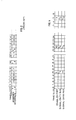
- FIG 2 a typical 32-slot time frame is shown together with some possible interfaces assigned to selected slots. Two of the slots (in this instance 0 and 16) are usually used for control functions and are thus unavailable. These slots have been labeled n. Hence in time slot No. 2 interface 13 is given access to both buses, time slot No. 3, is alloted to interface 25 and so on. However if interface 13 (time slot 2) is to exchange data with interface 7 (time slot 6), the data from time slot No. 2 of the Tx bus must be placed in time slot No. 6 of the Rx bus and vice versa. This is accomplished by a rather complex switching system comprising read/write control logic circuit 30 and random access memory 32 interconnected as shown in Figure 1.
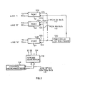
- a plurality'of lines 1, 2...N are connected to communication ports 102, 104, 108 respectively.
- the communication ports each have an input port 103 and an output port 105 for connection to the Rx and Tx buses respectively.
- the term communication port is used generically to represent any of a number of known interface devices for interfacing with subscriber lines, trunk lines, or other switching systems.
- the actual member of lines connected to the system is determined by the desired traffic handling capability, number of time slots and the speed of the Tx and Rx buses.
- Signals from the respective lines are transferred by the communication ports to Tx bus 110. Signals to the respective lines are transferred by the communication ports from Rx bus 112.
- a control microprocessor 114 sends appropriate signals on a low speed control bus 116 to a strobe generator 118. The strobe generator in turn generates control signals S 1 ...S n for communication ports 102, 104...108 during the appropriate time slots.
- FIG. 3 shows a single strobe generator providing control signals to all of the communication ports. In order to conserve back plane wiring separate strobe generators could be provided in each communication port. In such a case the control bus 116 would be directed to the individual communication ports.
- the Tx bus 110 is connected to an Rx bus 112 by a simple delay circuit 120 which is adapted to provide a delay equal to one half of the frame period. If a frame is T seconds, delay circuit 120 generates a T/2 second time delay. The effect of the delay circuit is to generate a fixed relationship between all the times during which the signals appear on the slots of the Tx and Rx buses.
- Microprocessor 114 is adapted to always assign to the two ports which are to be connected, time slots which are T/2 seconds or one half frame apart.
- port 3 if there are 32 time slots per frame and port 3 (calling) requests connection to port 10, port 3 is assigned the first available slot, such as for example slot 5 and port 10 (called) is assigned the time slot which occurs one half frame after time slot 5.
- a signal S 3 from port 3 is transferred to Tx bus 110 during time slot 5 and is delayed one half frame and is then transferred to the Rx bus 112 as time slot 21 occurs and port 10 (called) is enabled and receives signal S3.
- a signal S 10 from port 10 (called) is transferred to Tx bus 110 during slot 21 and is delayed one half frame or 16 time slots before being transferred to the Rx bus 112 as time slot 5 of the next frame occurs when port 3 (calling) is again enabled to receive the signal S10 from port 10 (called) via Rx bus 112 and to simultaneously transfer a new signal to the Tx bus 110.
- the delay circuit 120 is fairly simple to implement. It may comprise, for example an X/2 bit serial-to-serial shift register which merely shifts serials the data from bus 110 to bus 112.
- the communication ports may be subscriber line interface circuits. Details of a typical line interface circuit are shown in Figure 5. It comprises a buffer stage 130, and a hybrid transformer network 132 for a 2-to-4 wire conversion. A pair of Rx (Receive) wire 134 and a pair of Tx (Transmit) wires 136 are connected between hybrid network 132 and A/D, D/A converter 138 as shown. The converter converts the analog signals from line 1 on wires 136 into PCM-encoded digital signals which are then transferred to Tx bus 110 through a switch 142. Similarly the PCM digital signals from Rx bus 112 are received at switch 142 and are fed to the line circuits where they are converted into analog signals which are then sent on wires 134 to the analog subscriber line.
- Converters such as A/D, D/A converter 138 are well known in the art and are described in U.S. Patents No. 4,161,633 and 4,270,027. The converter could also be used to convert the signals to PAM-encoded signals as opposed to PCM-encoded signals.
- the buffer 130, converter 138, ring relay 140 and switch 142 receive appropriate control signals from a control circuit 144 which receives control signals from control bus 116.
- a ring signal is generated on the subscriber line by activating ring relay 140 by an appropriate signal from the control microprocessor.
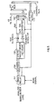
- a line interface circuit is shown for a digital subscriber line.
- the circuit 202 comprises a buffer 204 and a hybrid transformer network 206 for 2-to-4 wire conversion.
- a pair of Tx wires 208 are used to load the incoming signals from the subscriber line to a first serial-to-parallel register 210.
- Tx wires 208 are also connected to a circuit 212 provided to determine the clock timing of the incoming digital signals.
- the signals from register 210 are synchronously loaded into a first latch 214 using the recovered clock timing.
- a system control circuit 215 receives signals from the control microprocessor on control bus 116 which are used to transfer the data from latch 214 to a second latch 216.
- latches 214 and 216 are used to compensate for the phase difference between the digital subscriber line and the switching network.
- the PCM signals are transferred into a serial-to-parallel shift register 222.
- shift register 222 the data is transferred to a third latch 224 in accordance to system timing circuit 215.
- latch 224 the data is transferred to fourth latch 226 and from latch 226 to another parallel to serial shift register 228 in accordance with control signals from control circuit 215.
- register 228 the data outgoing signals are transferred by Rx wires 230 to hybrid transformer 206 and then back to the subscriber line.
- the switching or strobing function necessary to transfer signals to the Tx bus and receive signals from the Rx bus is accomplished by the control circuit 215 in conjunction with the latch which allows signals to shift out or in.
- the switching system described herein is well suited for a relatively small digital system such as a PABX.
- Various circuits could be added to perform various auxiliary functions.
- a 400 Hz signal generator could be used as a signal source to feed to slot No. 0 of the Tx bus.
- This slot or channel may then be used to generate "call progress signalling" (dial tone, busy tone, ring back, etc.).
- "call-in-progress" signal (busy tone) may be generated whenever one line attempts to access a second line and the second line is already engaged. In such a case the first line would be assigned to slot 16 of the Rx bus (in a 32-slot frame system) to receive said 400 Hz signal.
- Cadencing the tone on the assigned time slot-to generate the desired "Call Progress Signal” is done simply by periodically enabling and disabling the line interface 102, 104, 108 at a rate determined by the microprocessor 114.
- circuits which could be added are ringing circuits, ring-back circuits, pulse and/or tone dialing signal detect circuits and so on. These circuits are well known in the art and need not be described in greater detail.
Abstract
Description
- This invention pertains to a switching system which provides communication between a plurality of ports, and more particularly to a system having a common bus over which signals are exchanged between said ports by a time division multiplexing technique.
- Various switching networks have been proposed for high speed switching of digital and/or analog signals between a plurality of lines. As the number of lines connected to each network and data transmission increased these networks became more and more complex. Moreover as the amount of information being processed approaches the maximum capacity of a particular network, internal blocking also became frequent. The following United States Patents disclose some of these problems and suggest various solutions thereto.
- U.S. Patent No. 3,694,580 to Inose et al discloses a typical switching system in which two time division multiplexed buses are used as a data transfer means. The PCM signals on the buses are partitioned into frames, each frame comprising a plurality of channels of 8 bit intervals. The bit intervals are further subdivided into minibit intervals. The information contained in these minibit intervals are individually transferred from one bus to another by a complicated scheme in which the contents of some of the minibits of a particular frame are exchanged by delaying them to avoid blocking. A memory is used to keep track of the bits.
- U.S. Patent No. 3,740,483 to Pedersen also pertains to a switching network in which various time slots in a given frame are interchanged as the frame propagates from one stage of the network to the next. As a particular bit stream progresses from line A to line B it may be subject to both space switching and time switching. However, in full duplex communication a corresponding bit stream also progresses from B to A. Since the two paths are complementary, Pedersen eliminates some redundancy by using a bilateral time slot exchanger and a control memory having a single control word to control the interchange of the bit streams in either direction between any two lines.
- U.S. Patent No. 3,787,631 to Lewis discloses a system comprising a plurality of stations interconnected by a control time division switching network. At the beginning of each transmission each station requests a time slot from the control network. The central network detects the first idle time slot in the frame and assigns it to the requesting station. Each station actually takes the time slot following the designated time slot to compensate for various computational delays of the central network.
- U.S. Patent No. 3,920,916 to Brightman et al discloses a digital switching network interconnecting a large number of send and receive circuits by time division multiplexing. Send and receive memory means are used for temporarily storing the data while a proper time slot is assigned to each send/receive pair by a control circuit. The send memory means can transmit data in any sequence ordered by the control circuit. Furthermore a special duplex circuit is provided for two-way communication between a particular circuit pair.
- An objective of the present invention is to provide a switching system which consists of a minimum number of components so that it is easy to trouble shoot and inexpensive.
- Yet a further objective is to provide a system adapted to handle analog or digital signals.
- Another further objective is to provide a simple but effective time slot interchanger.
- Other objectives and advantages shall become apparent from the following description of the invention. _
- According to the present invention, a switching system comprises a plurality of communication ports through which communication signals are received and transmitted. The purpose of the switching system is to transfer selectively a signal from any one port to any other port. To this end the signals are transferred by the respective ports (after suitable conversion if necessary) to a TRANSMIT (Tx) bus in a time multiplexed fashion such as by using pulse-coded modulation (PCM). Similarly all the signals from a RECEIVE (Rx) bus are received at a port in time multiplexed fashion. Other forms of modulation could also be used such as pulse amplitude modulation (PAM).
- The communication ports may take many forms. They may be line interface circuits connecting subscriber lines to a switching system or trunk line interface circuits connecting trunks to a switching system. The communication ports could also be junctors that interconnect switching systems directly.
- Each port accesses the Tx and Rx buses only during a time slot so designated by a controller. The signals on the Tx bus must be delayed and transferred to the Rx bus so that they are received by the proper port when it accesses the Rx bus during its designated time slot. This is accomplished by delaying the Tx bus by one half of a frame period and then feeding the same to the Rx bus. The time slots assigned to the communication ports which communicate with each other differ by the same half-frame period. A frame period is the time that elapses between the start of the time slots during which a particular port accesses the buses.
-
- Figure 1 shows schematically a prior art digital switching network;
- Figure 2 shows a typical TDM frame slot assignment for the network of Figure 1;
- Figure 3 shows a network structured in accordance with the present invention;
- Figure 4 shows a typical TDM frame slot assignment for the system of Figure 3;
- Figure 5 shows details of an interface circuit for analog subscriber lines; and
- Figure 6 shows details of an interface circuit for a digital subscriber lines.
- A typical prior art switching system is shown in Figure 1 in a schematic form. This system is known as the ITT 1240 Digital Exchange and has been fully described in ELECTRICAL COMMUNICATION,
Volume 56,Number 2/3, 1981, pp. 135-160 as well as U.S. Patents No. 4,201,891: 4,293,946 and 4,317,962. This system has been selected because it can be easily adapted to perform in accordance with the subject invention. Briefly the system comprises a plurality ofline interface circuits subscriber lines bus 22. A time division multiplexing scheme is used whereby a time frame is divided into X or more time slots. A control microprocessor 24 is used to assign time slots to each line interface circuit. During the time slot alotted to a particular interface circuit, the circuit simultaneously accesses both the Tx and the Rx buses. Control microprocessor 24 assigns to each interface circuit requesting access to another circuit the first available time slot so that at any given time the assignment of each slot is rather random. The control microprocessor sends the designated time slot information to astrobe generator 26 over control bus 28. The strobe generator then provides control signals which enable each line interface during the appropriate time slot to allow access to the buses. - In Figure 2, a typical 32-slot time frame is shown together with some possible interfaces assigned to selected slots. Two of the slots (in this
instance 0 and 16) are usually used for control functions and are thus unavailable. These slots have been labeled n. Hence in time slot No. 2interface 13 is given access to both buses, time slot No. 3, is alloted to interface 25 and so on. However if interface 13 (time slot 2) is to exchange data with interface 7 (time slot 6), the data from time slot No. 2 of the Tx bus must be placed in time slot No. 6 of the Rx bus and vice versa. This is accomplished by a rather complex switching system comprising read/writecontrol logic circuit 30 andrandom access memory 32 interconnected as shown in Figure 1. - The present inventors have found that for small systems, i.e. systems with up to 200 subscriber lines, the complex switching system and time slot interchanger are not required if a system as shown in Figure 3 is used.
- The principles of operation of the present invention are illustrated in Figures 3 and 4. A
plurality'of lines communication ports input port 103 and anoutput port 105 for connection to the Rx and Tx buses respectively. It is to be understood that the term communication port is used generically to represent any of a number of known interface devices for interfacing with subscriber lines, trunk lines, or other switching systems. The actual member of lines connected to the system is determined by the desired traffic handling capability, number of time slots and the speed of the Tx and Rx buses. - Signals from the respective lines are transferred by the communication ports to
Tx bus 110. Signals to the respective lines are transferred by the communication ports fromRx bus 112. Acontrol microprocessor 114 sends appropriate signals on a low speed control bus 116 to astrobe generator 118. The strobe generator in turn generates control signals S1...Sn forcommunication ports - The communication ports in response to the control signals access both the Tx and Rx buses. Figure 3 shows a single strobe generator providing control signals to all of the communication ports. In order to conserve back plane wiring separate strobe generators could be provided in each communication port. In such a case the control bus 116 would be directed to the individual communication ports.
- However, instead of a complex switching system, the
Tx bus 110 is connected to anRx bus 112 by asimple delay circuit 120 which is adapted to provide a delay equal to one half of the frame period. If a frame is T seconds,delay circuit 120 generates a T/2 second time delay. The effect of the delay circuit is to generate a fixed relationship between all the times during which the signals appear on the slots of the Tx and Rx buses.Microprocessor 114 is adapted to always assign to the two ports which are to be connected, time slots which are T/2 seconds or one half frame apart. - Referring to Figure 4, if there are 32 time slots per frame and port 3 (calling) requests connection to
port 10,port 3 is assigned the first available slot, such as forexample slot 5 and port 10 (called) is assigned the time slot which occurs one half frame aftertime slot 5. Thus, a signal S3 fromport 3 is transferred toTx bus 110 duringtime slot 5 and is delayed one half frame and is then transferred to theRx bus 112 as time slot 21 occurs and port 10 (called) is enabled and receives signal S3. Similarly, a signal S10 from port 10 (called) is transferred toTx bus 110 during slot 21 and is delayed one half frame or 16 time slots before being transferred to theRx bus 112 astime slot 5 of the next frame occurs when port 3 (calling) is again enabled to receive the signal S10 from port 10 (called) viaRx bus 112 and to simultaneously transfer a new signal to theTx bus 110. - Importantly since the frame is automatically cycled for each bus, the information between
ports port 10 is transferred toport 3. Thus full duplex communication is provided by the system of Figure 3. - The
delay circuit 120 is fairly simple to implement. It may comprise, for example an X/2 bit serial-to-serial shift register which merely shifts serials the data frombus 110 tobus 112. - As previously mentioned the communication ports may be subscriber line interface circuits. Details of a typical line interface circuit are shown in Figure 5. It comprises a
buffer stage 130, and ahybrid transformer network 132 for a 2-to-4 wire conversion. A pair of Rx (Receive)wire 134 and a pair of Tx (Transmit)wires 136 are connected betweenhybrid network 132 and A/D, D/Aconverter 138 as shown. The converter converts the analog signals fromline 1 onwires 136 into PCM-encoded digital signals which are then transferred toTx bus 110 through aswitch 142. Similarly the PCM digital signals fromRx bus 112 are received atswitch 142 and are fed to the line circuits where they are converted into analog signals which are then sent onwires 134 to the analog subscriber line. Converters such as A/D, D/Aconverter 138 are well known in the art and are described in U.S. Patents No. 4,161,633 and 4,270,027. The converter could also be used to convert the signals to PAM-encoded signals as opposed to PCM-encoded signals. Thebuffer 130,converter 138,ring relay 140 and switch 142 receive appropriate control signals from a control circuit 144 which receives control signals from control bus 116. - A ring signal is generated on the subscriber line by activating
ring relay 140 by an appropriate signal from the control microprocessor. - In Figure 6, a line interface circuit is shown for a digital subscriber line. The
circuit 202 comprises abuffer 204 and ahybrid transformer network 206 for 2-to-4 wire conversion. A pair ofTx wires 208 are used to load the incoming signals from the subscriber line to a first serial-to-parallel register 210.Tx wires 208 are also connected to acircuit 212 provided to determine the clock timing of the incoming digital signals. The signals fromregister 210 are synchronously loaded into afirst latch 214 using the recovered clock timing. Asystem control circuit 215 receives signals from the control microprocessor on control bus 116 which are used to transfer the data fromlatch 214 to asecond latch 216. Thus latches 214 and 216 are used to compensate for the phase difference between the digital subscriber line and the switching network. - From
latch 216 the data is fed to a parallel-to-serial shift register 218 which feeds the data toTx bus 110. - Similarly, from
Rx bus 112 the PCM signals are transferred into a serial-to-parallel shift register 222. Fromshift register 222 the data is transferred to athird latch 224 in accordance tosystem timing circuit 215. Fromlatch 224 the data is transferred tofourth latch 226 and fromlatch 226 to another parallel toserial shift register 228 in accordance with control signals fromcontrol circuit 215. Fromregister 228 the data outgoing signals are transferred byRx wires 230 tohybrid transformer 206 and then back to the subscriber line. The switching or strobing function necessary to transfer signals to the Tx bus and receive signals from the Rx bus is accomplished by thecontrol circuit 215 in conjunction with the latch which allows signals to shift out or in. - The switching system described herein is well suited for a relatively small digital system such as a PABX. Various circuits could be added to perform various auxiliary functions. For example a 400 Hz signal generator could be used as a signal source to feed to slot No. 0 of the Tx bus. This slot or channel may then be used to generate "call progress signalling" (dial tone, busy tone, ring back, etc.). For example a "call-in-progress" signal (busy tone) may be generated whenever one line attempts to access a second line and the second line is already engaged. In such a case the first line would be assigned to slot 16 of the Rx bus (in a 32-slot frame system) to receive said 400 Hz signal.
- Cadencing the tone on the assigned time slot-to generate the desired "Call Progress Signal" is done simply by periodically enabling and disabling the
line interface microprocessor 114. - Other circuits which could be added are ringing circuits, ring-back circuits, pulse and/or tone dialing signal detect circuits and so on. These circuits are well known in the art and need not be described in greater detail.
- Furthermore one skilled in the art could make other modifications to the described invention without departing from its scope as defined in the appended claims.
Claims (16)
Applications Claiming Priority (2)
| Application Number | Priority Date | Filing Date | Title |
|---|---|---|---|
| US653754 | 1984-09-21 | ||
| US06/653,754 US4601029A (en) | 1984-09-21 | 1984-09-21 | Communication switching system |
Publications (2)
| Publication Number | Publication Date |
|---|---|
| EP0176437A2 true EP0176437A2 (en) | 1986-04-02 |
| EP0176437A3 EP0176437A3 (en) | 1988-10-05 |
Family
ID=24622177
Family Applications (1)
| Application Number | Title | Priority Date | Filing Date |
|---|---|---|---|
| EP85401825A Withdrawn EP0176437A3 (en) | 1984-09-21 | 1985-09-19 | Communication switching system |
Country Status (6)
| Country | Link |
|---|---|
| US (1) | US4601029A (en) |
| EP (1) | EP0176437A3 (en) |
| JP (1) | JPS6180994A (en) |
| BE (1) | BE903289A (en) |
| CA (1) | CA1238968A (en) |
| ES (1) | ES8707058A1 (en) |
Cited By (3)
| Publication number | Priority date | Publication date | Assignee | Title |
|---|---|---|---|---|
| GB2219714A (en) * | 1988-06-10 | 1989-12-13 | Heikki Malkki | Telephone systems |
| EP0663743A1 (en) * | 1993-12-27 | 1995-07-19 | Mitsubishi Denki Kabushiki Kaisha | Time-division multiplexer with reduced delay time |
| GB2326305A (en) * | 1997-06-13 | 1998-12-16 | Schlumberger Ind Ltd | Local exchange testing |
Families Citing this family (10)
| Publication number | Priority date | Publication date | Assignee | Title |
|---|---|---|---|---|
| US4710769A (en) * | 1985-12-30 | 1987-12-01 | Ibm Corporation | Transmit-secure non-blocking circuit-switched local area network |
| US4800558A (en) * | 1987-03-03 | 1989-01-24 | Pathfinder Systems, Inc. | Telephone switching system frame sync generator |
| US5088089A (en) * | 1989-12-15 | 1992-02-11 | Alcatel Na Network Systems Corp. | Apparatus for programmably accessing and assigning time slots in a time division multiplexed communication system |
| US5331632A (en) * | 1992-01-31 | 1994-07-19 | At&T Bell Laboratories | Expandable time slot interchanger |
| JP2541747B2 (en) * | 1993-03-31 | 1996-10-09 | 日本電気株式会社 | Communication switching system |
| US6259703B1 (en) | 1993-10-22 | 2001-07-10 | Mitel Corporation | Time slot assigner for communication system |
| US5940402A (en) * | 1997-06-06 | 1999-08-17 | Timeplex, Inc. | Method and apparatus for TDM interrupt transmissions between multiple devices and a processor |
| JP3061016B2 (en) * | 1997-10-29 | 2000-07-10 | 日本電気株式会社 | PCM highway extension method |
| US6463074B1 (en) | 2000-06-14 | 2002-10-08 | Tantivy Communications, Inc. | Receiver for time division multiplex system without explicit time slot assignment |
| US6845104B2 (en) * | 2000-06-14 | 2005-01-18 | Ipr Licensing, Inc. | Receiver for time division multiplex system without explicit time slot assignment |
Family Cites Families (4)
| Publication number | Priority date | Publication date | Assignee | Title |
|---|---|---|---|---|
| US3732374A (en) * | 1970-12-31 | 1973-05-08 | Ibm | Communication system and method |
| US4140877A (en) * | 1977-04-19 | 1979-02-20 | Tie/Communications, Inc. | Muliple highway time division multiplexed PABX communication system |
| US4488290A (en) * | 1982-08-04 | 1984-12-11 | M/A-Com Linkabit, Inc. | Distributed digital exchange with improved switching system and input processor |
| JPS5954347A (en) * | 1982-09-22 | 1984-03-29 | Fujitsu Ltd | System for adjusting timing of channel insertion |
-
1984
- 1984-09-21 US US06/653,754 patent/US4601029A/en not_active Expired - Fee Related
-
1985
- 1985-09-19 EP EP85401825A patent/EP0176437A3/en not_active Withdrawn
- 1985-09-20 ES ES547165A patent/ES8707058A1/en not_active Expired
- 1985-09-20 JP JP60206771A patent/JPS6180994A/en active Granted
- 1985-09-20 CA CA000491291A patent/CA1238968A/en not_active Expired
- 1985-09-23 BE BE2/60800A patent/BE903289A/en not_active IP Right Cessation
Non-Patent Citations (4)
| Title |
|---|
| CONFERENCE ON ELECTRONIC TELEPHONE EXCHANGES, London, 22nd-23rd November 1960, vol. 107, part B, supplement 20, paper 3465 E, pages 81-87; P.W. WARD et al.: "The trunking of 100-channel T.D.M. exchanges" * |
| IRE TRANSACTIONS ON COMMUNICATIONS SYSTEMS, vol. 10, no. 4, December 1962, pages 397-407, New York, US; H. INOSE et al.: "The subscriber-line circuit and the signaling and tone system for an experimental time-division exchange featuring delta-modulation techniques" * |
| NACHRICHTENTECHNIK ELEKTRONIK, vol. 17, no. 5, May 1967, pages 188-191, Berlin, DE; J. HRADEK et al.: "Probleme des Vierdraht-Zeitmultiplex-Betriebes in der EATZ" * |
| PROCEEDINGS OF THE INSTITUTION OF ELECTRICAL ENGINEERS, vol. 103, no. 12, part B, 1956, pages 722-736, London, GB; L.R.F. HARRIS: "Time sharing as a basis for electronic telephone switching" * |
Cited By (6)
| Publication number | Priority date | Publication date | Assignee | Title |
|---|---|---|---|---|
| GB2219714A (en) * | 1988-06-10 | 1989-12-13 | Heikki Malkki | Telephone systems |
| US5027347A (en) * | 1988-06-10 | 1991-06-25 | Heikki Malkki | Intercom system |
| GB2219714B (en) * | 1988-06-10 | 1992-10-28 | Heikki Malkki | Intercom system |
| EP0663743A1 (en) * | 1993-12-27 | 1995-07-19 | Mitsubishi Denki Kabushiki Kaisha | Time-division multiplexer with reduced delay time |
| US5521920A (en) * | 1993-12-27 | 1996-05-28 | Mitsubishi Denki Kabushiki Kaisha | Time-division multiplexer with reduced delay time |
| GB2326305A (en) * | 1997-06-13 | 1998-12-16 | Schlumberger Ind Ltd | Local exchange testing |
Also Published As
| Publication number | Publication date |
|---|---|
| ES8707058A1 (en) | 1987-07-01 |
| EP0176437A3 (en) | 1988-10-05 |
| ES547165A0 (en) | 1987-07-01 |
| CA1238968A (en) | 1988-07-05 |
| US4601029A (en) | 1986-07-15 |
| JPH0230239B2 (en) | 1990-07-05 |
| BE903289A (en) | 1986-01-16 |
| JPS6180994A (en) | 1986-04-24 |
Similar Documents
| Publication | Publication Date | Title |
|---|---|---|
| US4322843A (en) | Control information communication arrangement for a time division switching system | |
| US4704716A (en) | Method and apparatus for establishing a wideband communication facility through a communication network having narrow bandwidth channels | |
| US4382294A (en) | Telephone switching control arrangement | |
| US4173713A (en) | Continuously expandable switching network | |
| CA1150805A (en) | Time division switching system control arrangement | |
| BE903857R (en) | TELECOMMUNCATION SWITCHING SYSTEM AND PRIORITY DEVICE APPLIED THEREIN. | |
| US4460994A (en) | Loop communication system | |
| US4601029A (en) | Communication switching system | |
| US4885738A (en) | Method of and apparatus for establishing a wideband communication facility through a switched communications network having narrow bandwidth time division multiplexed channels | |
| GB2074815A (en) | Telecommunications switching network using digital switching modules | |
| US4296492A (en) | Continuity verification arrangement | |
| US3925621A (en) | Digital circuit switched time-space-time switch equipped time division transmission loop system | |
| US4287590A (en) | Time division multiplex communication system | |
| EP0114822B1 (en) | Communication arrangements for distributed control systems | |
| US4484324A (en) | Control information communication arrangement for a time division switching system | |
| CA1210841A (en) | Time-space-time switching network using a closed-loop link | |
| US3660605A (en) | Pulse code modulation switching system utilizing tasi | |
| US3846587A (en) | Data transmission system for a multiple branch network | |
| US4602363A (en) | Expansion apparatus for use in communication systems | |
| US4868812A (en) | Shared lines equipment, especially for B-ISDN switching system | |
| US4628502A (en) | Data and signaling time slot transfer and processing system for a set of multiplex lines | |
| US4143241A (en) | Small digital time division switching arrangement | |
| CA1083696A (en) | Time division switching network | |
| US4194090A (en) | Decentralized-control type electronic switching system | |
| US3641272A (en) | Time division automatic telephone switching equipment |
Legal Events
| Date | Code | Title | Description |
|---|---|---|---|
| PUAI | Public reference made under article 153(3) epc to a published international application that has entered the european phase |
Free format text: ORIGINAL CODE: 0009012 |
|
| AK | Designated contracting states |
Kind code of ref document: A2 Designated state(s): CH DE FR GB IT LI SE |
|
| RBV | Designated contracting states (corrected) |
Designated state(s): CH DE FR GB IT LI |
|
| RAP1 | Party data changed (applicant data changed or rights of an application transferred) |
Owner name: ALCATEL N.V. |
|
| RAP3 | Party data changed (applicant data changed or rights of an application transferred) |
Owner name: ALCATEL N.V. |
|
| PUAL | Search report despatched |
Free format text: ORIGINAL CODE: 0009013 |
|
| AK | Designated contracting states |
Kind code of ref document: A3 Designated state(s): CH DE FR GB IT LI |
|
| STAA | Information on the status of an ep patent application or granted ep patent |
Free format text: STATUS: THE APPLICATION IS DEEMED TO BE WITHDRAWN |
|
| 18D | Application deemed to be withdrawn |
Effective date: 19890406 |
|
| RIN1 | Information on inventor provided before grant (corrected) |
Inventor name: HARGRAVE, FRANKLIN Inventor name: MIDDLETON, FRANCISCO ARTURO |