EP0173523B1 - Optical memory - Google Patents
Optical memory Download PDFInfo
- Publication number
- EP0173523B1 EP0173523B1 EP85305854A EP85305854A EP0173523B1 EP 0173523 B1 EP0173523 B1 EP 0173523B1 EP 85305854 A EP85305854 A EP 85305854A EP 85305854 A EP85305854 A EP 85305854A EP 0173523 B1 EP0173523 B1 EP 0173523B1
- Authority
- EP
- European Patent Office
- Prior art keywords
- recording layer
- memory device
- optical memory
- layer
- optical
- Prior art date
- Legal status (The legal status is an assumption and is not a legal conclusion. Google has not performed a legal analysis and makes no representation as to the accuracy of the status listed.)
- Expired - Lifetime
Links
- 230000003287 optical effect Effects 0.000 title claims description 82
- 230000015654 memory Effects 0.000 title description 23
- 239000010410 layer Substances 0.000 claims description 126
- 239000004065 semiconductor Substances 0.000 claims description 50
- 239000000758 substrate Substances 0.000 claims description 34
- 239000000463 material Substances 0.000 claims description 33
- WPYVAWXEWQSOGY-UHFFFAOYSA-N indium antimonide Chemical compound [Sb]#[In] WPYVAWXEWQSOGY-UHFFFAOYSA-N 0.000 claims description 18
- 230000008859 change Effects 0.000 claims description 17
- 239000003989 dielectric material Substances 0.000 claims description 14
- 239000011241 protective layer Substances 0.000 claims description 12
- 238000001704 evaporation Methods 0.000 claims description 8
- 238000000034 method Methods 0.000 claims description 8
- 230000002441 reversible effect Effects 0.000 claims description 8
- 229910052802 copper Inorganic materials 0.000 claims description 4
- 230000005670 electromagnetic radiation Effects 0.000 claims description 4
- 229910052737 gold Inorganic materials 0.000 claims description 4
- 229910052709 silver Inorganic materials 0.000 claims description 4
- 238000004544 sputter deposition Methods 0.000 claims description 4
- 230000001678 irradiating effect Effects 0.000 claims description 3
- 229910001632 barium fluoride Inorganic materials 0.000 claims description 2
- WUKWITHWXAAZEY-UHFFFAOYSA-L calcium difluoride Chemical compound [F-].[F-].[Ca+2] WUKWITHWXAAZEY-UHFFFAOYSA-L 0.000 claims description 2
- 229910001634 calcium fluoride Inorganic materials 0.000 claims description 2
- 239000002131 composite material Substances 0.000 claims description 2
- 229910001635 magnesium fluoride Inorganic materials 0.000 claims description 2
- 230000008569 process Effects 0.000 claims description 2
- 229910052782 aluminium Inorganic materials 0.000 claims 1
- 229910052814 silicon oxide Inorganic materials 0.000 claims 1
- 238000002310 reflectometry Methods 0.000 description 28
- 239000010408 film Substances 0.000 description 22
- 239000002245 particle Substances 0.000 description 21
- 238000000151 deposition Methods 0.000 description 13
- 230000008021 deposition Effects 0.000 description 12
- 230000007704 transition Effects 0.000 description 10
- 229910052714 tellurium Inorganic materials 0.000 description 8
- 238000001579 optical reflectometry Methods 0.000 description 6
- 239000011347 resin Substances 0.000 description 6
- 229920005989 resin Polymers 0.000 description 6
- PORWMNRCUJJQNO-UHFFFAOYSA-N tellurium atom Chemical compound [Te] PORWMNRCUJJQNO-UHFFFAOYSA-N 0.000 description 6
- 230000000694 effects Effects 0.000 description 5
- 230000006870 function Effects 0.000 description 5
- 239000000203 mixture Substances 0.000 description 5
- 239000010409 thin film Substances 0.000 description 4
- VYPSYNLAJGMNEJ-UHFFFAOYSA-N Silicium dioxide Chemical compound O=[Si]=O VYPSYNLAJGMNEJ-UHFFFAOYSA-N 0.000 description 3
- 238000010276 construction Methods 0.000 description 3
- 239000011248 coating agent Substances 0.000 description 2
- 238000000576 coating method Methods 0.000 description 2
- 238000010586 diagram Methods 0.000 description 2
- 238000010438 heat treatment Methods 0.000 description 2
- 230000007246 mechanism Effects 0.000 description 2
- 229920000515 polycarbonate Polymers 0.000 description 2
- 239000004417 polycarbonate Substances 0.000 description 2
- 229920005668 polycarbonate resin Polymers 0.000 description 2
- 239000004431 polycarbonate resin Substances 0.000 description 2
- 230000004044 response Effects 0.000 description 2
- 239000000126 substance Substances 0.000 description 2
- 239000004925 Acrylic resin Substances 0.000 description 1
- 229920000178 Acrylic resin Polymers 0.000 description 1
- 229910011255 B2O3 Inorganic materials 0.000 description 1
- -1 BiF3 Chemical class 0.000 description 1
- 230000004075 alteration Effects 0.000 description 1
- GHPGOEFPKIHBNM-UHFFFAOYSA-N antimony(3+);oxygen(2-) Chemical compound [O-2].[O-2].[O-2].[Sb+3].[Sb+3] GHPGOEFPKIHBNM-UHFFFAOYSA-N 0.000 description 1
- 229910052681 coesite Inorganic materials 0.000 description 1
- 230000001427 coherent effect Effects 0.000 description 1
- 239000000470 constituent Substances 0.000 description 1
- 238000001816 cooling Methods 0.000 description 1
- 238000005260 corrosion Methods 0.000 description 1
- 230000007797 corrosion Effects 0.000 description 1
- 229910052906 cristobalite Inorganic materials 0.000 description 1
- 230000001419 dependent effect Effects 0.000 description 1
- FPHIOHCCQGUGKU-UHFFFAOYSA-L difluorolead Chemical compound F[Pb]F FPHIOHCCQGUGKU-UHFFFAOYSA-L 0.000 description 1
- 230000008020 evaporation Effects 0.000 description 1
- 150000002222 fluorine compounds Chemical class 0.000 description 1
- 239000011521 glass Substances 0.000 description 1
- 239000012535 impurity Substances 0.000 description 1
- YEXPOXQUZXUXJW-UHFFFAOYSA-N lead(II) oxide Inorganic materials [Pb]=O YEXPOXQUZXUXJW-UHFFFAOYSA-N 0.000 description 1
- 230000031700 light absorption Effects 0.000 description 1
- 238000004519 manufacturing process Methods 0.000 description 1
- 239000002184 metal Substances 0.000 description 1
- 229910052751 metal Inorganic materials 0.000 description 1
- 230000010287 polarization Effects 0.000 description 1
- 230000009467 reduction Effects 0.000 description 1
- 235000012239 silicon dioxide Nutrition 0.000 description 1
- 239000000377 silicon dioxide Substances 0.000 description 1
- 239000007787 solid Substances 0.000 description 1
- 229910052682 stishovite Inorganic materials 0.000 description 1
- 229910052718 tin Inorganic materials 0.000 description 1
- 230000009466 transformation Effects 0.000 description 1
- 238000000844 transformation Methods 0.000 description 1
- 239000012780 transparent material Substances 0.000 description 1
- 229910052905 tridymite Inorganic materials 0.000 description 1
- 238000007738 vacuum evaporation Methods 0.000 description 1
Images


Classifications
-
- G—PHYSICS
- G11—INFORMATION STORAGE
- G11B—INFORMATION STORAGE BASED ON RELATIVE MOVEMENT BETWEEN RECORD CARRIER AND TRANSDUCER
- G11B7/00—Recording or reproducing by optical means, e.g. recording using a thermal beam of optical radiation by modifying optical properties or the physical structure, reproducing using an optical beam at lower power by sensing optical properties; Record carriers therefor
- G11B7/24—Record carriers characterised by shape, structure or physical properties, or by the selection of the material
- G11B7/241—Record carriers characterised by shape, structure or physical properties, or by the selection of the material characterised by the selection of the material
- G11B7/252—Record carriers characterised by shape, structure or physical properties, or by the selection of the material characterised by the selection of the material of layers other than recording layers
- G11B7/257—Record carriers characterised by shape, structure or physical properties, or by the selection of the material characterised by the selection of the material of layers other than recording layers of layers having properties involved in recording or reproduction, e.g. optical interference layers or sensitising layers or dielectric layers, which are protecting the recording layers
-
- G—PHYSICS
- G11—INFORMATION STORAGE
- G11B—INFORMATION STORAGE BASED ON RELATIVE MOVEMENT BETWEEN RECORD CARRIER AND TRANSDUCER
- G11B7/00—Recording or reproducing by optical means, e.g. recording using a thermal beam of optical radiation by modifying optical properties or the physical structure, reproducing using an optical beam at lower power by sensing optical properties; Record carriers therefor
- G11B7/24—Record carriers characterised by shape, structure or physical properties, or by the selection of the material
- G11B7/241—Record carriers characterised by shape, structure or physical properties, or by the selection of the material characterised by the selection of the material
- G11B7/242—Record carriers characterised by shape, structure or physical properties, or by the selection of the material characterised by the selection of the material of recording layers
- G11B7/243—Record carriers characterised by shape, structure or physical properties, or by the selection of the material characterised by the selection of the material of recording layers comprising inorganic materials only, e.g. ablative layers
- G11B7/2433—Metals or elements of groups 13, 14, 15 or 16 of the Periodic System, e.g. B, Si, Ge, As, Sb, Bi, Se or Te
-
- G—PHYSICS
- G11—INFORMATION STORAGE
- G11B—INFORMATION STORAGE BASED ON RELATIVE MOVEMENT BETWEEN RECORD CARRIER AND TRANSDUCER
- G11B7/00—Recording or reproducing by optical means, e.g. recording using a thermal beam of optical radiation by modifying optical properties or the physical structure, reproducing using an optical beam at lower power by sensing optical properties; Record carriers therefor
- G11B7/004—Recording, reproducing or erasing methods; Read, write or erase circuits therefor
- G11B7/0055—Erasing
- G11B7/00557—Erasing involving phase-change media
-
- G—PHYSICS
- G11—INFORMATION STORAGE
- G11B—INFORMATION STORAGE BASED ON RELATIVE MOVEMENT BETWEEN RECORD CARRIER AND TRANSDUCER
- G11B7/00—Recording or reproducing by optical means, e.g. recording using a thermal beam of optical radiation by modifying optical properties or the physical structure, reproducing using an optical beam at lower power by sensing optical properties; Record carriers therefor
- G11B7/24—Record carriers characterised by shape, structure or physical properties, or by the selection of the material
- G11B7/241—Record carriers characterised by shape, structure or physical properties, or by the selection of the material characterised by the selection of the material
- G11B7/242—Record carriers characterised by shape, structure or physical properties, or by the selection of the material characterised by the selection of the material of recording layers
- G11B7/243—Record carriers characterised by shape, structure or physical properties, or by the selection of the material characterised by the selection of the material of recording layers comprising inorganic materials only, e.g. ablative layers
-
- G—PHYSICS
- G11—INFORMATION STORAGE
- G11B—INFORMATION STORAGE BASED ON RELATIVE MOVEMENT BETWEEN RECORD CARRIER AND TRANSDUCER
- G11B7/00—Recording or reproducing by optical means, e.g. recording using a thermal beam of optical radiation by modifying optical properties or the physical structure, reproducing using an optical beam at lower power by sensing optical properties; Record carriers therefor
- G11B7/24—Record carriers characterised by shape, structure or physical properties, or by the selection of the material
- G11B7/26—Apparatus or processes specially adapted for the manufacture of record carriers
-
- G—PHYSICS
- G11—INFORMATION STORAGE
- G11B—INFORMATION STORAGE BASED ON RELATIVE MOVEMENT BETWEEN RECORD CARRIER AND TRANSDUCER
- G11B7/00—Recording or reproducing by optical means, e.g. recording using a thermal beam of optical radiation by modifying optical properties or the physical structure, reproducing using an optical beam at lower power by sensing optical properties; Record carriers therefor
- G11B7/24—Record carriers characterised by shape, structure or physical properties, or by the selection of the material
- G11B7/241—Record carriers characterised by shape, structure or physical properties, or by the selection of the material characterised by the selection of the material
- G11B7/242—Record carriers characterised by shape, structure or physical properties, or by the selection of the material characterised by the selection of the material of recording layers
- G11B7/243—Record carriers characterised by shape, structure or physical properties, or by the selection of the material characterised by the selection of the material of recording layers comprising inorganic materials only, e.g. ablative layers
- G11B2007/24302—Metals or metalloids
- G11B2007/2431—Metals or metalloids group 13 elements (B, Al, Ga, In)
-
- G—PHYSICS
- G11—INFORMATION STORAGE
- G11B—INFORMATION STORAGE BASED ON RELATIVE MOVEMENT BETWEEN RECORD CARRIER AND TRANSDUCER
- G11B7/00—Recording or reproducing by optical means, e.g. recording using a thermal beam of optical radiation by modifying optical properties or the physical structure, reproducing using an optical beam at lower power by sensing optical properties; Record carriers therefor
- G11B7/24—Record carriers characterised by shape, structure or physical properties, or by the selection of the material
- G11B7/241—Record carriers characterised by shape, structure or physical properties, or by the selection of the material characterised by the selection of the material
- G11B7/242—Record carriers characterised by shape, structure or physical properties, or by the selection of the material characterised by the selection of the material of recording layers
- G11B7/243—Record carriers characterised by shape, structure or physical properties, or by the selection of the material characterised by the selection of the material of recording layers comprising inorganic materials only, e.g. ablative layers
- G11B2007/24302—Metals or metalloids
- G11B2007/24312—Metals or metalloids group 14 elements (e.g. Si, Ge, Sn)
-
- G—PHYSICS
- G11—INFORMATION STORAGE
- G11B—INFORMATION STORAGE BASED ON RELATIVE MOVEMENT BETWEEN RECORD CARRIER AND TRANSDUCER
- G11B7/00—Recording or reproducing by optical means, e.g. recording using a thermal beam of optical radiation by modifying optical properties or the physical structure, reproducing using an optical beam at lower power by sensing optical properties; Record carriers therefor
- G11B7/24—Record carriers characterised by shape, structure or physical properties, or by the selection of the material
- G11B7/241—Record carriers characterised by shape, structure or physical properties, or by the selection of the material characterised by the selection of the material
- G11B7/242—Record carriers characterised by shape, structure or physical properties, or by the selection of the material characterised by the selection of the material of recording layers
- G11B7/243—Record carriers characterised by shape, structure or physical properties, or by the selection of the material characterised by the selection of the material of recording layers comprising inorganic materials only, e.g. ablative layers
- G11B2007/24302—Metals or metalloids
- G11B2007/24314—Metals or metalloids group 15 elements (e.g. Sb, Bi)
-
- G—PHYSICS
- G11—INFORMATION STORAGE
- G11B—INFORMATION STORAGE BASED ON RELATIVE MOVEMENT BETWEEN RECORD CARRIER AND TRANSDUCER
- G11B7/00—Recording or reproducing by optical means, e.g. recording using a thermal beam of optical radiation by modifying optical properties or the physical structure, reproducing using an optical beam at lower power by sensing optical properties; Record carriers therefor
- G11B7/24—Record carriers characterised by shape, structure or physical properties, or by the selection of the material
- G11B7/241—Record carriers characterised by shape, structure or physical properties, or by the selection of the material characterised by the selection of the material
- G11B7/242—Record carriers characterised by shape, structure or physical properties, or by the selection of the material characterised by the selection of the material of recording layers
- G11B7/243—Record carriers characterised by shape, structure or physical properties, or by the selection of the material characterised by the selection of the material of recording layers comprising inorganic materials only, e.g. ablative layers
- G11B2007/24302—Metals or metalloids
- G11B2007/24316—Metals or metalloids group 16 elements (i.e. chalcogenides, Se, Te)
-
- G—PHYSICS
- G11—INFORMATION STORAGE
- G11B—INFORMATION STORAGE BASED ON RELATIVE MOVEMENT BETWEEN RECORD CARRIER AND TRANSDUCER
- G11B7/00—Recording or reproducing by optical means, e.g. recording using a thermal beam of optical radiation by modifying optical properties or the physical structure, reproducing using an optical beam at lower power by sensing optical properties; Record carriers therefor
- G11B7/24—Record carriers characterised by shape, structure or physical properties, or by the selection of the material
- G11B7/241—Record carriers characterised by shape, structure or physical properties, or by the selection of the material characterised by the selection of the material
- G11B7/252—Record carriers characterised by shape, structure or physical properties, or by the selection of the material characterised by the selection of the material of layers other than recording layers
- G11B7/257—Record carriers characterised by shape, structure or physical properties, or by the selection of the material characterised by the selection of the material of layers other than recording layers of layers having properties involved in recording or reproduction, e.g. optical interference layers or sensitising layers or dielectric layers, which are protecting the recording layers
- G11B2007/25705—Record carriers characterised by shape, structure or physical properties, or by the selection of the material characterised by the selection of the material of layers other than recording layers of layers having properties involved in recording or reproduction, e.g. optical interference layers or sensitising layers or dielectric layers, which are protecting the recording layers consisting essentially of inorganic materials
- G11B2007/25706—Record carriers characterised by shape, structure or physical properties, or by the selection of the material characterised by the selection of the material of layers other than recording layers of layers having properties involved in recording or reproduction, e.g. optical interference layers or sensitising layers or dielectric layers, which are protecting the recording layers consisting essentially of inorganic materials containing transition metal elements (Zn, Fe, Co, Ni, Pt)
-
- G—PHYSICS
- G11—INFORMATION STORAGE
- G11B—INFORMATION STORAGE BASED ON RELATIVE MOVEMENT BETWEEN RECORD CARRIER AND TRANSDUCER
- G11B7/00—Recording or reproducing by optical means, e.g. recording using a thermal beam of optical radiation by modifying optical properties or the physical structure, reproducing using an optical beam at lower power by sensing optical properties; Record carriers therefor
- G11B7/24—Record carriers characterised by shape, structure or physical properties, or by the selection of the material
- G11B7/241—Record carriers characterised by shape, structure or physical properties, or by the selection of the material characterised by the selection of the material
- G11B7/252—Record carriers characterised by shape, structure or physical properties, or by the selection of the material characterised by the selection of the material of layers other than recording layers
- G11B7/257—Record carriers characterised by shape, structure or physical properties, or by the selection of the material characterised by the selection of the material of layers other than recording layers of layers having properties involved in recording or reproduction, e.g. optical interference layers or sensitising layers or dielectric layers, which are protecting the recording layers
- G11B2007/25705—Record carriers characterised by shape, structure or physical properties, or by the selection of the material characterised by the selection of the material of layers other than recording layers of layers having properties involved in recording or reproduction, e.g. optical interference layers or sensitising layers or dielectric layers, which are protecting the recording layers consisting essentially of inorganic materials
- G11B2007/25708—Record carriers characterised by shape, structure or physical properties, or by the selection of the material characterised by the selection of the material of layers other than recording layers of layers having properties involved in recording or reproduction, e.g. optical interference layers or sensitising layers or dielectric layers, which are protecting the recording layers consisting essentially of inorganic materials containing group 13 elements (B, Al, Ga)
-
- G—PHYSICS
- G11—INFORMATION STORAGE
- G11B—INFORMATION STORAGE BASED ON RELATIVE MOVEMENT BETWEEN RECORD CARRIER AND TRANSDUCER
- G11B7/00—Recording or reproducing by optical means, e.g. recording using a thermal beam of optical radiation by modifying optical properties or the physical structure, reproducing using an optical beam at lower power by sensing optical properties; Record carriers therefor
- G11B7/24—Record carriers characterised by shape, structure or physical properties, or by the selection of the material
- G11B7/241—Record carriers characterised by shape, structure or physical properties, or by the selection of the material characterised by the selection of the material
- G11B7/252—Record carriers characterised by shape, structure or physical properties, or by the selection of the material characterised by the selection of the material of layers other than recording layers
- G11B7/257—Record carriers characterised by shape, structure or physical properties, or by the selection of the material characterised by the selection of the material of layers other than recording layers of layers having properties involved in recording or reproduction, e.g. optical interference layers or sensitising layers or dielectric layers, which are protecting the recording layers
- G11B2007/25705—Record carriers characterised by shape, structure or physical properties, or by the selection of the material characterised by the selection of the material of layers other than recording layers of layers having properties involved in recording or reproduction, e.g. optical interference layers or sensitising layers or dielectric layers, which are protecting the recording layers consisting essentially of inorganic materials
- G11B2007/2571—Record carriers characterised by shape, structure or physical properties, or by the selection of the material characterised by the selection of the material of layers other than recording layers of layers having properties involved in recording or reproduction, e.g. optical interference layers or sensitising layers or dielectric layers, which are protecting the recording layers consisting essentially of inorganic materials containing group 14 elements except carbon (Si, Ge, Sn, Pb)
-
- G—PHYSICS
- G11—INFORMATION STORAGE
- G11B—INFORMATION STORAGE BASED ON RELATIVE MOVEMENT BETWEEN RECORD CARRIER AND TRANSDUCER
- G11B7/00—Recording or reproducing by optical means, e.g. recording using a thermal beam of optical radiation by modifying optical properties or the physical structure, reproducing using an optical beam at lower power by sensing optical properties; Record carriers therefor
- G11B7/24—Record carriers characterised by shape, structure or physical properties, or by the selection of the material
- G11B7/241—Record carriers characterised by shape, structure or physical properties, or by the selection of the material characterised by the selection of the material
- G11B7/252—Record carriers characterised by shape, structure or physical properties, or by the selection of the material characterised by the selection of the material of layers other than recording layers
- G11B7/257—Record carriers characterised by shape, structure or physical properties, or by the selection of the material characterised by the selection of the material of layers other than recording layers of layers having properties involved in recording or reproduction, e.g. optical interference layers or sensitising layers or dielectric layers, which are protecting the recording layers
- G11B2007/25705—Record carriers characterised by shape, structure or physical properties, or by the selection of the material characterised by the selection of the material of layers other than recording layers of layers having properties involved in recording or reproduction, e.g. optical interference layers or sensitising layers or dielectric layers, which are protecting the recording layers consisting essentially of inorganic materials
- G11B2007/25715—Record carriers characterised by shape, structure or physical properties, or by the selection of the material characterised by the selection of the material of layers other than recording layers of layers having properties involved in recording or reproduction, e.g. optical interference layers or sensitising layers or dielectric layers, which are protecting the recording layers consisting essentially of inorganic materials containing oxygen
-
- Y—GENERAL TAGGING OF NEW TECHNOLOGICAL DEVELOPMENTS; GENERAL TAGGING OF CROSS-SECTIONAL TECHNOLOGIES SPANNING OVER SEVERAL SECTIONS OF THE IPC; TECHNICAL SUBJECTS COVERED BY FORMER USPC CROSS-REFERENCE ART COLLECTIONS [XRACs] AND DIGESTS
- Y10—TECHNICAL SUBJECTS COVERED BY FORMER USPC
- Y10S—TECHNICAL SUBJECTS COVERED BY FORMER USPC CROSS-REFERENCE ART COLLECTIONS [XRACs] AND DIGESTS
- Y10S430/00—Radiation imagery chemistry: process, composition, or product thereof
- Y10S430/146—Laser beam
Landscapes
- Chemical & Material Sciences (AREA)
- Inorganic Chemistry (AREA)
- Engineering & Computer Science (AREA)
- Manufacturing & Machinery (AREA)
- Optical Record Carriers And Manufacture Thereof (AREA)
- Thermal Transfer Or Thermal Recording In General (AREA)
Description
- The present invention relates to an optical memory which is capable of storing and retrieving information by light exposure. More specifically, the invention relates to an optical recording disc comprising a recording layer that has an optical property which changes when the layer is irradiated with electromagnetic radiation such as light from a laser.
- For storing and retrieving information, an optical disc comprising a layer or film of semiconductor materials is widely used in industrial and consumer recording systems such as video recorders, digital audio recorders and document digital recorders. A signal is recorded on the optical disc by applying a laser beam so that bits of information are formed in a layer of semiconductor material. The optical disc permits direct read after write and random access to the recorded information.
- Layers of certain semiconductor materials, such as Se, Ge, Te and InSb, are known for their ability to assume two stable states, amorphous and crystalline. The concept of an optical memory based on the amorphous-to-crystalline transition of the semiconductor materials mentioned above is disclosed by S.R. Ovshinsky et al, "Reversible Structural Transformations in Amorphous Semiconductors for Memory and Logic", METALLURGICAL TRANS. 2:641-45 (1971). These semiconductor materials, however, are chemically unstable and are gradually corroded in the air when they are made into a thin film. Therefore, they are not used in practice as the recording film of an optical disc memory.
- Since 1971, substantial effort has been expended to produce a durable recording film of semiconductor materials. For example, in "Reversible Optical Recording in Trilayer Structures" APPL.PHYS. LETT. 38:920-921 (1981), A. E. Bell et al disclose an erasable optical recording medium based on the amorphous-to-crystalline transition of pure tellurium. The optical recording disc of Bell et al includes silicon dioxide capping layers formed on the both sides of the tellurium film to protect the pure tellurium film from corrosion and to prevent the tellurium from evaporating. In the resulting trilayer structures, the thickness of each layer must be precisely controlled, making the film forming-process unduly complicated.
- Another example of an optical disc is reported by M. Takenaga in Proceedings of the 116th Study Meeting of No. 131 Film Conference of the Japan Society for the Promotion of Science, May 20, 1983, at pp. 21-26. This optical disc is based on the reversible transition of a tellurium sub-oxide thin film which is formed as a deposition layer by simultaneous evaporation of Te02 and Te that contains Ge or Sn as an impurity. Therefore, it is difficult to control the quality of the film produced via the disclosed method, because the method includes decomposing unstable Te02 at a high temperature. Moreover, the tellurium sub-oxide thin film has a low reflectivity (about 15%) and a low rate of reflectivity change (about 12%), resulting in a low signal-to-noise (SN) ratio.
- Further guidance concerning the state of the art may be obtained by reference to FR-A-2507805 which discloses an optical recording device in which the recording domains consisting e.g. of Te or Se within a chemical stable material, can be switched reversibly between a substantially (but not wholly) crystalline phase and a substantially (but not wholly) amorphous phase. Each phase having different optical reflectivity.
- However, the device of FR-A-2507805 can not store data with an entirely satisfactory signal to noise ratio. Claim 1 of the present application acknowledges FR-A-2507805 in the precharacterising portion.
- Accordingly, the present invention seeks to provide an improved optical memory wherein data can be optically stored and retrieved with a satisfactory signal to noise ratio.
- In accordance with the present invention there is provided an optical memory device comprising a substrate and a recording layer supported thereon, said recording layer consisting of a composite of chemically stable dielectric material and domains of a semi-conductor material which undergo a reversible crystalline phase change when irradiated by electromagnetic radiation each phase having different optical characteristics characterised in that the semi-conductor material comprises at least one of Ge or InSb whereby the semi-conductor material can be induced to undergo a completely reversible change between a wholly amorphous and a wholly crystalline phase, in accordance with the duration and intensity with which the device is irradiated by electromagnetic radiation.
- Some embodiments of the present invention will now be described by way of example only with reference to the accompanying drawings in which:
- Figures 1 through 3 each provide a sectional view, respectively, of different configurations of optical discs according to the present invention;
- Figure 4 is a schematic diagram depicting a coevaporation system for use in preparing an optical disc memory with the present invention;
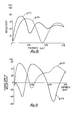
- Figures 5, and 10 are graphs showing, respectively, the relationship between the rate of reflectivity change and the thickness of recording films of the present invention;
- Figures 6 and 8 are graphs both showing the relationship between the reflectivity and the thickness of recording films of the present invention;
- Figure 7 is a graph showing the relationship between the reflectivity of a recording film of the present invention and exposure time; and
- Figure 11 is a schematic diagram of an optical disc memory system within the present invention.
- The
optical discs transparent substrate Substrate grooves 18 and can be rotated.Grooves 18, as shown in Figure 1, are formed on the surface ofsubstrate substrate 16' or 16".Grooves 18 are used for optical tracking, in that portions to record or erase information are guided as a recording track by the grooves. - The optical disc has a recording layer or
film dielectric member - The semiconductor material used in the present invention preferably has a fractional volume factor of about 40% or more, where fractional volume factor (q) is defined as the ratio of the volume of the semiconductor material in the recording layer to the total volume of the recording layer. Also, in the present description "chemically stable dielectric member" denotes a dielectric material that is effectively unreactive with the aforesaid semiconductor material and doe not interfere with a light-modulated phase transition within the semiconductor particles, as further detailed below.
- A light beam is employed to heat semiconductor particles in selected regions of the recording layer. For example, recording
film semiconductor particles - The semiconductor particles in the irradiated portions of the recording film are thus cooled quickly when heated by irradiation with a high power density beam for a short time and, conversely, are cooled slowly when heated by an irradiating beam of a lower power density for a longer time. Moreover, the semiconductor particles become amorphous in structure when they are heated by irradiation with a high power density beam for a short time and cooled quickly. Conversely, they enter a crystalline phase when they are heated by irradiation with a lower power density beam for a longer time and cooled slowly. The use of semiconductor particles for reversible recording is based on a transition in the structure of the particles which occurs when the particles are heated and, as a consequence, have different optical properties (i.e., reflectivity) characterized by the complex refractive index. More specifically,
semiconductor particles recording layer recording layer - A particularly preferred optical thickness for
recording film film film semiconductor particles dielectric member - In another embodiment of the present invention, the surface of
optical disc memory protective layer protective layer - With reference to Figure 1,
optical disc memory 10 comprisessubstrate 16, anoverlying recording layer 20, and aprotective layer 26 adjacent to the recording layer. Laser beam L is applied to recordinglayer 20 throughtransparent substrate 16 and reflected at both boundaries of the recording layer, so that the reflected light R is changed in its intensity according to the reflectivity of the recording layer. - With reference to Figure 2,
optical disc memory 12 comprises substrate 16', recording layer 20' formed on substrate 16',metallic layer 28 formed on recording layer 20' and protective layer 26' formed onmetallic layer 28.Metallic layer 28 is comprised of Cu and has a high reflectivity. Recording layer 20' is irradiated by laser beam L through transparent substrate 16'. The impinging laser light is reflected at the surface of recording layer 20' and the surface ofmetallic layer 28, respectively, and the intensity of reflected light is changed as a function of the reflectivity of the recording layer. In this embodiment,metallic layer 28 is particularly desirable because of its high reflectivity. Such a structure assures a reading operation characterized by a high SN ratio, since constructive interference between reflected rays R, R' and R" enhances signal intensity. - With reference to Figure 3,
optical disc memory 14 has a semitransparentmetallic layer 30 comprised of Cu which is interposed betweensubstrate 16" andrecording layer 20". The optical disc memory also has a metallic layer 28' which is similartometallic layer 28 shown in Figure 2. Thus, in this embodimentoptical disc memory 14 comprisessubstrate 16", semitransparentmetallic layer 30 formed onsubstrate 16",recording layer 20" formed on semitransparentmetallic layer 30, metallic layer 28' formed onrecording layer 20" andprotective layer 26" formed on metallic layer 28'. Recordinglayer 20" is exposed to laser beam L throughsubstrate 16" and semitransparentmetallic layer 30, so that the light R is reflected at the surfaces of semitransparentmetallic layer 30,recording layer 20" and metallic layer 28', respectively. As a result, the reflected light is changed in its intensity according to the reflectivity ofrecording layer 20". This multilayer structure enables the intensity of the reflected light R to be twice that ofoptical disc 12 shown in Figure 2, because of an interference effect involving rays reflected, respectively, by the multiple layers. - Semiconductor materials such as Ge, Te, Se, and InSb are well-known fortheir ability to assume two different phases (amorphous and crystalline) according to the manner of heating. Moreover, dielectric materials that are suitableforthe present invention must have sufficient chemical stability, as defined above, to prevent semiconductor materials from evaporating and corroding. For example, oxides, such as
B 203, Sb2O3, PbO, Si02 and Ta2o5, and fluorides, such as BiF3, LiF, PbF2, MgF2, BaF2 and CaF2, are suitable for the dielectric member of the present invention. - The fractional volume factor of semiconductor particles in the present invention is preferably more than about 40% of the mixture of semiconductor materials and dielectric materials, and particularly is in the range of about 40 to 80%, to obtain sufficient reflectivity and durability for the optical disc memory. By preparing the mixture mentioned above, the recording layer works satisfactorily as an optical interference film although semiconductor materials generally have a high absorbancy.
- Methods based on vacuum evaporation, sputtering and the like can be used to prepare both the recording layer and the metallic layer of the present invention. For example, a multilayered structure as described above is achieved using the co-evaporating apparatus shown in Figure 4. A
deposition chamber 32 containssubstrate member 34 and rotated by a motor 36. Disposed below supportingmember 34 areheaters heaters Deposition chamber 32 is connected to avacuum pump 46 so that the deposition chamber can be evacuated to a pressure of about 10-3 Pa. - Cleaned
substrate member 34, with the cleaned surface kept downward, and is rotated by motor 36.Pump 46 is then operated so as to bring the pressure ofdeposition chamber 32 down to about 10-3 Pa. Thenheaters - After the completion of the deposition, a valve (not shown) is opened to break the vacuum in
deposition chamber 32. The prepared disc is removed from the apparatus and coated with a UV-curable resin, which forms the protective layer upon being irradiated with UV light. - The present invention will be described further with reference to the following illustrative examples.
- In accordance with the procedure described below, an optical disc memory of the present invention was prepared by using an apparatus as shown in Figure 4.
- A substrate comprising polycarbonate resins was provided in the form of a disc having a diameter of about 130 mm and a thickness of about 1.2 mm and carrying grooves thereon of 0.07 11m in depth and 0.8 µm in width. The substrate was cleaned and fixed to supporting
member 34. Then, the substrate was rotated andheaters deposition chamber 32.Heater 38 heated Ge andheater 40 heated Bi103 (for a dielectric material member). A recording layer comprising a mixture of Ge andBi 203 was formed by simultaneously evaporating Ge andBi 203 onto the substrate, such that the fractional volume factor of Ge in the whole recording layer was adjusted via power source 44 to about 60%. - The disc was covered with a protective layer made of UV-cured resin, so that it had a multi- layered structure as shown in Figure 1. The resulting optical disc displayed an optical reflectivity that changed upon exposure of the disc to a laser beam having a wavelength of 0.83 pm. As shown in Figure 5, when the recording layer was exposed by the laser beam with wavelength of 0.83 pm and the phase of the recording layer was thereby irreversibly switched from amorphous to crystalline, or vice versa, the observed rate of reflectivity change depended on the thickness of the recording layer. Disc reflectivity was likewise a function of the thickness of the recording layer, as shown in Figure 6.
- The results illustrated in Figures 5 and 6 indicate that the thickness of the recording layer should be about 0.05 µm, i.e., in the range where disc reflectivity and reflectivity change-of-rate underwent significant alteration in response to exposure depending on the above-mentioned optical interference effect, and strong readout signals were obtainable.
- An optical disc was prepared as described in Example 1, except that InSb was used for the semiconductor material and PbO for the dielectric material. In addition, the thickess of the recording layer was adjusted to 1 pm, and no protective layer was employed.
- To test durability, the optical disc thus obtained was exposed to high temperature and humidity conditions. As shown in Figure 7, the results indicated that fractional volume factor q of about 0.4 to 0.8 was associated with superior durability and reflectivity characteristics. When the recording layer comprising InSb and PbO was scanned by a laser beam of 0.83 µm wavelength, the reflectivity of the recording layer was observed to be a function of both the thickness of the recording layer and the fractional volume factor q of InSb (see Figure 8).
- Accordingly, the value for fractional volume factor q is preferably selected between about 0.4 (40%) to 0.8 (80%). If this condition is satisfied, semiconductor material having a high absorbancy works satisfactorily as a constituent of an optical interference film also comprising a suitable dielectric material. Moreover, the optical interference of reflected light at both boundaries of the recording layer can be increased because of the reduction of absorbency associated with the reduced fractional volume factor q.
- An optical disc was prepared as in Example 2, using the apparatus illustrated in Figure 4. More specifically, a polycarbonate, disc-shaped substrate having a thickness of about 1.2 mm and a diameter of about 130 mm was cleaned and fixed to supporting
member 34. The substrate was then rotated andheaters deposition chamber 32 was kept at a high vacuum.Heaters -
Heaters heater 42 was operated to heat Cu. As a result, a metallic layer having a thickness of about 0.05 µm was formed on the recording layer. After completion of the Cu deposition, the substrate was removed from the apparatus and was coated with UV-curable resins; a protective layer was thereafter formed on the metallic layer by irradiating the resin coating with UV light. - The resulting optical disc displayed an optical reflectivity that changed upon exposure of the disc to a laser beam having a wavelength of about 0.83 11m. As shown in Figure 9, the disc also showed a rate of reflectivity change that depended on the thickness of the recording layer. In the light of the data shown in Figure 9, the thickness of the recording layer was preferably about 0.055 µm.
- In Figure 9, the dotted line represents the case when fractional volume factor q was 1.0, that is, the recording layer consisted essentially of InSb. The curves for q=1.0 and q=0.6, respectively, show almost the same rate of reflectivity change, i.e., strong read-out signals were obtained with the multi-layered disc construction even when InSb content was reduced from 100% to about 60%.
- To obtain the multilayered structure shown in Figure 2, the recording layer is formed by simultaneous sputtering, whereby discrete semiconductor regions are dispersed within the chemically stable dielectric member. The semiconductor regions dispersed in the recording layer can easily change to amorphous or crystalline phase, and the important feature of recording layer durability is dramatically enhanced. The deposition of the metallic layer by sputtering also makes the fabrication operation simple.
- An optical disc was prepared as described in the Example 3, except that the fractional volume factor of InSb was established at about 90% and Se was used as a dielectric material member. In addition, AI was used instead of Cu for the metallic layer. Thus, a recording layer comprised of InSb and Se was deposited on the substrate, and a metallic laer of AI was deposited on the recording layer. Next, a protective layer was applied so that the resulting optical disc had the multilayered construction shown in Figure 2. The thickness of the recording layer was in the range of about 0.04-0.08 pm, and the thickness of the metallic layer was about 0.05 um. The Se dielectric material was effectively transparent to the impinging laser beam, which had a wavelength of about 0.83 µm.
- The resulting multilayer optical disc underwent an amorphous-to-crystalline phase transition upon irradiation with the laser beam, and a large rate of reflectivity change was observed in conjunction with the phase transition. Furthermore, the durability of the recording layer was extremely improved.
- In the manner of Example 1, an optical disc memory was prepared, using the apparatus shown in Figure 4. A polycarbonate, disc-shaped substrate having a thickness of about 1.2 mm and a diameter of about 130 mm, and carrying grooves for optical tracking, was cleaned and fixed to supporting
member 34. The substrate was then rotated, andheater 42 operated to heat Cu, while the inside ofchamber 32 was kept at a high vacuum of 10-3 Pa. A semitransparent metallic layer having a thickness of about 0.01 11m was thereby deposited on the substrate.Heater 42 was then deenergised andheaters Heaters heater 42 was operated to heat Cu for depositing a second metallic layer, having a thickness of about 0.05 or more, on the recording layer. Finally a protective layer was coated on the second metallic layer. - The resulting optical disc displayed an optical reflectivity which changed when the disc was irradiated with a laser beam having a wavelength of 0.83 µm. As shown in Figure 10, the disc also showed a large rate of reflectivity change which was a function of recording layer thickness. Based on the results illustrated in Figure 10, the thickness of the recording layer was preferably about 0.07 µm.
- The optical disc described above had a rate of reflectivity change of about 80% or more, owing to the multilayered construction shown in Figure 3, i.e., to the optical interference effect of multipath reflection of light. Such a large rate of relectivity change permits one to regenerate information, recorded on the recording layer as the portions of different phases, with a high SN ratio.
- The optical disc described in the foregoing examples is used for an image recording medium for an image information filing apparatus as shown in Figure 11. The apparatus of Figure 11 comprises a
semiconductor laser diode 48 for reading and recording information and a semi-conductor laser diode 50 for erasing information recorded on the disc. The laser beam emitted fromdiode lens mirror 56. The light reflected frommirror 56 enters alens 58 and then is reflected by amirror 60. The reflected laser beam frommirror 60 is introduced to apolarizing beam splitter 62 and then to aplate 64 having a thickness such that the laser beam is retarded by one-quarter the wavelength of the applied laser beam. The laser beam enters then alens 66 and is thereby focused on the optical disc.Lens 66 is movably supported by a driving mechanism (not shown) to adjust radially and axially the position oflens 66.Optical disc - The light reflected from the optical disc enters
lens 66 again and passesplate 64. At this time, the polarization plane of the light is changed by 90° because the light moves back and forth withinplate 64, so that the light is reflected bypolarizing beam splitter 62 and deflected to a converginglens 68 and acolumn lens 70. The reflected light from the optical disc is detected by adetector 72.Lens 66 is moved by the driving mechanism so that the converged spot fromlens 66 focuses on the desired groove of the optical disc, i.e., the recording track is traced in response to the output signal ofdetector 72. - The laser diode emits the 0.83 pm wavelength laser beam in 0.15 pS pulses of about 7 mW in power when a recording operation is effected. In an erasing operation, the diode emits the beam in a 1.3 pS pulse of lower power, i.e., about 4 mW.
- When an optical disc memory of the present invention, which can have a multilayered structure as described in Example 3, is placed in the apparatus shown in Figure 11 and a reading operation is carried out,
laser diode 48 continuously emits a laser beam having one-third the power of a recording operation. The emitted light passes through the substrate and is reflected at both boundaries of the recording layer and the metallic layer, respectively. The intensity of the reflected light changes according to the reflectivity of the recorded portion, where the structure of the semiconductor particles has been switched to amorphous phase. Thus, the recorded inforam- tion is regenerated as a change of reflectivity. In an erasing operation,laser diode 50 continuously emits an erasing beam to which the optical disc is exposed, whereby the structure of the semiconductor particles is switched to crystalline phase and the recorded information is consequently erased. In a recording operation,laser diode 50 works continuously andlaser diode 48 emits pulsed light which contains information, so that the portions of the recording layer irradiated by the erasing beam and containing semiconductor particles in the cystalline phase are then switched to amorphous phase by the recording beam. The converged spot of the recording beam is smaller than that of the erasing beam and is guided on the recording track behind the spot of erasing beam, so that the operations of recording and erasing are executed simultaneously. - According to the present invention, the semi- conductor material is stabilized within the recording layer, even if the disc is broken in the handling, assuring safety. Moreover, the recording layer may be easily deposited by the above-described co-evaporating method, so that optical disc memories of uniform quality and moderate price can be produced. As described above, it is possible with the present invention to provide an improved optical memory that can optically, reversibly store and retrieve information, is excellent in durability, has a high contrast ratio, and can be prepared using a simple film-forming process.
Claims (13)
Applications Claiming Priority (4)
| Application Number | Priority Date | Filing Date | Title |
|---|---|---|---|
| JP176276/84 | 1984-08-24 | ||
| JP59176276A JPS6153090A (en) | 1984-08-24 | 1984-08-24 | Optical disk |
| JP59211964A JPS6190341A (en) | 1984-10-09 | 1984-10-09 | Optical disk |
| JP211964/84 | 1984-10-09 |
Publications (3)
| Publication Number | Publication Date |
|---|---|
| EP0173523A2 EP0173523A2 (en) | 1986-03-05 |
| EP0173523A3 EP0173523A3 (en) | 1987-07-29 |
| EP0173523B1 true EP0173523B1 (en) | 1990-11-07 |
Family
ID=26497258
Family Applications (1)
| Application Number | Title | Priority Date | Filing Date |
|---|---|---|---|
| EP85305854A Expired - Lifetime EP0173523B1 (en) | 1984-08-24 | 1985-08-16 | Optical memory |
Country Status (4)
| Country | Link |
|---|---|
| US (1) | US4969141A (en) |
| EP (1) | EP0173523B1 (en) |
| KR (1) | KR890004230B1 (en) |
| DE (1) | DE3580429D1 (en) |
Families Citing this family (29)
| Publication number | Priority date | Publication date | Assignee | Title |
|---|---|---|---|---|
| DE3675845D1 (en) * | 1985-08-15 | 1991-01-10 | Ibm | OPTICAL RECORDING PROCEDURE. |
| JPS63179425A (en) * | 1987-01-20 | 1988-07-23 | Fuji Photo Film Co Ltd | Optical information recording method and information recording medium tube used therein |
| JP2512087B2 (en) * | 1988-06-24 | 1996-07-03 | 株式会社日立製作所 | Optical recording medium and optical recording method |
| DE69127398T2 (en) * | 1990-05-22 | 1998-01-02 | Canon Kk | Method and apparatus for recording and reproducing information in cells that use multiple interference |
| US5666344A (en) * | 1991-06-04 | 1997-09-09 | International Business Machines Corporation | Multiple data surface optical data storage system |
| KR100242859B1 (en) * | 1991-06-20 | 2000-02-01 | 가나이 쓰도무 | Method of varying optical properties, optical devices, information recording media and information recording methods and apparatus |
| JPH0562239A (en) * | 1991-06-20 | 1993-03-12 | Hitachi Ltd | Recording medium and information recording method by using this medium |
| US5485452A (en) * | 1991-06-28 | 1996-01-16 | Pioneer Electronic Corporation | Optical information recording medium |
| EP0611473B1 (en) * | 1991-10-03 | 1997-05-02 | Del Mar Avionics | Optical disc master |
| US5253198A (en) * | 1991-12-20 | 1993-10-12 | Syracuse University | Three-dimensional optical memory |
| US5194980A (en) * | 1992-05-29 | 1993-03-16 | Eastman Kodak Company | Thresholded, high power laser beam scanning system |
| JPH0628713A (en) * | 1992-07-13 | 1994-02-04 | Pioneer Electron Corp | Optical disk |
| US5864530A (en) * | 1993-01-04 | 1999-01-26 | U.S. Philips Corporation | Multiplane information storage system and record carrier for use in such a system |
| US5474874A (en) * | 1993-02-16 | 1995-12-12 | Sony Corporation | Optical recording medium |
| CN1054227C (en) * | 1994-10-31 | 2000-07-05 | 北京航空航天大学 | High-order nonlinear optical-hysteresis bistable material and optical disc and card using said material |
| JPH08329525A (en) * | 1995-03-27 | 1996-12-13 | Hitachi Ltd | Information recording medium and information memory device |
| US5889756A (en) * | 1996-07-25 | 1999-03-30 | Kabushiki Kaisha Toshiba | Phase change optical recording medium |
| US5825725A (en) * | 1997-05-06 | 1998-10-20 | The State Of Oregon Acting By And Through The State Board Of Higher Education On Behalf Of The University Of Oregon | Method and apparatus for reversible optical data storage |
| JP4537528B2 (en) * | 2000-03-29 | 2010-09-01 | 株式会社東芝 | Optical recording medium |
| EP1393309A1 (en) * | 2001-04-12 | 2004-03-03 | Koninklijke Philips Electronics N.V. | Rewritable optical data storage medium and use of such a medium |
| JP4006994B2 (en) * | 2001-12-18 | 2007-11-14 | 株式会社リコー | Three-dimensional structure processing method, three-dimensional product manufacturing method, and three-dimensional structure |
| TWI256629B (en) * | 2002-06-03 | 2006-06-11 | Tdk Corp | Optical recording/reproduction method and optical recording medium |
| TWI263993B (en) * | 2002-06-03 | 2006-10-11 | Tdk Corp | Optical recording reproduction method and optical recording medium |
| JP4047074B2 (en) * | 2002-06-03 | 2008-02-13 | Tdk株式会社 | Optical recording / reproducing method and optical recording medium |
| FR2848014A1 (en) * | 2002-12-03 | 2004-06-04 | Commissariat Energie Atomique | Irreversible optical recording support comprises alloy of tellurium and zinc with an additional metal layer for heat dissipation |
| TWI245288B (en) * | 2003-03-20 | 2005-12-11 | Sony Corp | Semiconductor memory element and semiconductor memory device using the same |
| WO2005023553A1 (en) * | 2003-09-05 | 2005-03-17 | Nec Corporation | Optical information recording medium and optical information recording/reproducing apparatus |
| JP5225372B2 (en) * | 2008-04-01 | 2013-07-03 | 株式会社東芝 | Information recording / reproducing device |
| JP5300839B2 (en) * | 2008-04-15 | 2013-09-25 | 株式会社東芝 | Information recording / reproducing device |
Family Cites Families (11)
| Publication number | Priority date | Publication date | Assignee | Title |
|---|---|---|---|---|
| EP0045183B1 (en) * | 1980-07-25 | 1984-12-05 | Asahi Kasei Kogyo Kabushiki Kaisha | Recording material |
| FR2488711B1 (en) * | 1980-08-13 | 1985-06-28 | Thomson Csf | THERMO-OPTICAL INFORMATION RECORDING PROCESS AND INFORMATION MEDIUM FOR CARRYING OUT SAID METHOD |
| JPS57205193A (en) * | 1981-06-12 | 1982-12-16 | Fuji Photo Film Co Ltd | Optical information recording medium |
| US4425570A (en) * | 1981-06-12 | 1984-01-10 | Rca Corporation | Reversible recording medium and information record |
| US4465767A (en) * | 1981-11-27 | 1984-08-14 | Ricoh Company, Ltd. | Optical information recording medium |
| JPS58121149A (en) * | 1981-12-22 | 1983-07-19 | Fujitsu Ltd | Recording medium |
| JPS5960744A (en) * | 1982-09-30 | 1984-04-06 | Ricoh Co Ltd | Photomagnetic recording medium |
| EP0110730B1 (en) * | 1982-12-06 | 1988-05-11 | Plasmon Data Systems N.V. | Improvements relating to data storage and recording |
| JPS59104996A (en) * | 1982-12-08 | 1984-06-18 | Canon Inc | Optical recording medium |
| JPS59113534A (en) * | 1982-12-20 | 1984-06-30 | Canon Inc | Optical recording medium |
| US4576895A (en) * | 1984-06-18 | 1986-03-18 | International Business Machines Corporation | Optical recording by energy-induced fractionation and homogenization |
-
1985
- 1985-08-14 KR KR1019850005874A patent/KR890004230B1/en not_active IP Right Cessation
- 1985-08-16 EP EP85305854A patent/EP0173523B1/en not_active Expired - Lifetime
- 1985-08-16 DE DE8585305854T patent/DE3580429D1/en not_active Expired - Lifetime
-
1989
- 1989-04-18 US US07/339,656 patent/US4969141A/en not_active Expired - Fee Related
Also Published As
| Publication number | Publication date |
|---|---|
| EP0173523A3 (en) | 1987-07-29 |
| EP0173523A2 (en) | 1986-03-05 |
| KR860002088A (en) | 1986-03-26 |
| DE3580429D1 (en) | 1990-12-13 |
| US4969141A (en) | 1990-11-06 |
| KR890004230B1 (en) | 1989-10-27 |
Similar Documents
| Publication | Publication Date | Title |
|---|---|---|
| EP0173523B1 (en) | Optical memory | |
| US4924436A (en) | Data storage device having a phase change memory medium reversible by direct overwrite and method of direct overwrite | |
| US5481530A (en) | High density optical recording method and recording medium | |
| US4719594A (en) | Grooved optical data storage device including a chalcogenide memory layer | |
| US4425570A (en) | Reversible recording medium and information record | |
| JP3392706B2 (en) | Optical data storage system and optical data recording medium | |
| KR100770078B1 (en) | Multi-layered optical disc | |
| JP2512087B2 (en) | Optical recording medium and optical recording method | |
| US6469977B2 (en) | Optical information recording medium, method for producing the same, and method and apparatus for recording/reproducing information thereon | |
| US5521901A (en) | Re-writable phase change type optical disk with suppressed recording mark distortion | |
| GB2079031A (en) | Optical information record and a method of reversibly recording and erasing information thereon | |
| JPH0355893B2 (en) | ||
| US5631895A (en) | Optical information recording medium | |
| JP4339999B2 (en) | Optical information recording medium, manufacturing method thereof, recording / reproducing method, and recording / reproducing apparatus | |
| US4860274A (en) | Information storage medium and method of erasing information | |
| US5314734A (en) | Information-recording medium | |
| JPH09198709A (en) | Multilayered optical disk and recording and reproducing device | |
| US5811217A (en) | Optical information recording medium and optical information recording/reproducing method | |
| KR100753968B1 (en) | Rewritable optical information recording medium | |
| JP3012734B2 (en) | Optical information recording medium and structure design method thereof | |
| US4879205A (en) | Information storage medium and a method of manufacturing the same | |
| EP0307750B1 (en) | Use of a storage meedium in a method of recording information | |
| JP2993435B2 (en) | Optical information recording medium | |
| JPH07134838A (en) | Optical information recording medium and recording method | |
| JP2001028148A (en) | Optical information recording medium, its manufacture, recording/reproducing method and recording/ reproducing device |
Legal Events
| Date | Code | Title | Description |
|---|---|---|---|
| PUAI | Public reference made under article 153(3) epc to a published international application that has entered the european phase |
Free format text: ORIGINAL CODE: 0009012 |
|
| 17P | Request for examination filed |
Effective date: 19850829 |
|
| AK | Designated contracting states |
Kind code of ref document: A2 Designated state(s): DE FR GB NL |
|
| PUAL | Search report despatched |
Free format text: ORIGINAL CODE: 0009013 |
|
| AK | Designated contracting states |
Kind code of ref document: A3 Designated state(s): DE FR GB NL |
|
| 17Q | First examination report despatched |
Effective date: 19890523 |
|
| GRAA | (expected) grant |
Free format text: ORIGINAL CODE: 0009210 |
|
| AK | Designated contracting states |
Kind code of ref document: B1 Designated state(s): DE FR GB NL |
|
| ET | Fr: translation filed | ||
| REF | Corresponds to: |
Ref document number: 3580429 Country of ref document: DE Date of ref document: 19901213 |
|
| PLBE | No opposition filed within time limit |
Free format text: ORIGINAL CODE: 0009261 |
|
| STAA | Information on the status of an ep patent application or granted ep patent |
Free format text: STATUS: NO OPPOSITION FILED WITHIN TIME LIMIT |
|
| 26N | No opposition filed | ||
| PGFP | Annual fee paid to national office [announced via postgrant information from national office to epo] |
Ref country code: GB Payment date: 19940808 Year of fee payment: 10 |
|
| PGFP | Annual fee paid to national office [announced via postgrant information from national office to epo] |
Ref country code: FR Payment date: 19940809 Year of fee payment: 10 |
|
| PGFP | Annual fee paid to national office [announced via postgrant information from national office to epo] |
Ref country code: DE Payment date: 19940816 Year of fee payment: 10 |
|
| PGFP | Annual fee paid to national office [announced via postgrant information from national office to epo] |
Ref country code: NL Payment date: 19940831 Year of fee payment: 10 |
|
| PG25 | Lapsed in a contracting state [announced via postgrant information from national office to epo] |
Ref country code: GB Effective date: 19950816 |
|
| PG25 | Lapsed in a contracting state [announced via postgrant information from national office to epo] |
Ref country code: NL Effective date: 19960301 |
|
| GBPC | Gb: european patent ceased through non-payment of renewal fee |
Effective date: 19950816 |
|
| PG25 | Lapsed in a contracting state [announced via postgrant information from national office to epo] |
Ref country code: FR Effective date: 19960430 |
|
| NLV4 | Nl: lapsed or anulled due to non-payment of the annual fee |
Effective date: 19960301 |
|
| PG25 | Lapsed in a contracting state [announced via postgrant information from national office to epo] |
Ref country code: DE Effective date: 19960501 |
|
| REG | Reference to a national code |
Ref country code: FR Ref legal event code: ST |