EP0173445B1 - Power control circuit - Google Patents
Power control circuit Download PDFInfo
- Publication number
- EP0173445B1 EP0173445B1 EP85305201A EP85305201A EP0173445B1 EP 0173445 B1 EP0173445 B1 EP 0173445B1 EP 85305201 A EP85305201 A EP 85305201A EP 85305201 A EP85305201 A EP 85305201A EP 0173445 B1 EP0173445 B1 EP 0173445B1
- Authority
- EP
- European Patent Office
- Prior art keywords
- pulse width
- control signals
- switching devices
- control means
- output
- Prior art date
- Legal status (The legal status is an assumption and is not a legal conclusion. Google has not performed a legal analysis and makes no representation as to the accuracy of the status listed.)
- Expired - Lifetime
Links
- 238000006243 chemical reaction Methods 0.000 claims 2
- 238000010586 diagram Methods 0.000 description 4
- 238000004804 winding Methods 0.000 description 4
- 239000013078 crystal Substances 0.000 description 2
- 230000000694 effects Effects 0.000 description 2
- 230000003019 stabilising effect Effects 0.000 description 2
- 230000008878 coupling Effects 0.000 description 1
- 238000010168 coupling process Methods 0.000 description 1
- 238000005859 coupling reaction Methods 0.000 description 1
- 230000005669 field effect Effects 0.000 description 1
- 230000001939 inductive effect Effects 0.000 description 1
- 238000009434 installation Methods 0.000 description 1
- 238000004519 manufacturing process Methods 0.000 description 1
- 238000000034 method Methods 0.000 description 1
- 238000003079 width control Methods 0.000 description 1
Images


Classifications
-
- H—ELECTRICITY
- H02—GENERATION; CONVERSION OR DISTRIBUTION OF ELECTRIC POWER
- H02M—APPARATUS FOR CONVERSION BETWEEN AC AND AC, BETWEEN AC AND DC, OR BETWEEN DC AND DC, AND FOR USE WITH MAINS OR SIMILAR POWER SUPPLY SYSTEMS; CONVERSION OF DC OR AC INPUT POWER INTO SURGE OUTPUT POWER; CONTROL OR REGULATION THEREOF
- H02M7/00—Conversion of AC power input into DC power output; Conversion of DC power input into AC power output
- H02M7/42—Conversion of DC power input into AC power output without possibility of reversal
- H02M7/44—Conversion of DC power input into AC power output without possibility of reversal by static converters
- H02M7/48—Conversion of DC power input into AC power output without possibility of reversal by static converters using discharge tubes with control electrode or semiconductor devices with control electrode
- H02M7/53—Conversion of DC power input into AC power output without possibility of reversal by static converters using discharge tubes with control electrode or semiconductor devices with control electrode using devices of a triode or transistor type requiring continuous application of a control signal
- H02M7/537—Conversion of DC power input into AC power output without possibility of reversal by static converters using discharge tubes with control electrode or semiconductor devices with control electrode using devices of a triode or transistor type requiring continuous application of a control signal using semiconductor devices only, e.g. single switched pulse inverters
- H02M7/5387—Conversion of DC power input into AC power output without possibility of reversal by static converters using discharge tubes with control electrode or semiconductor devices with control electrode using devices of a triode or transistor type requiring continuous application of a control signal using semiconductor devices only, e.g. single switched pulse inverters in a bridge configuration
- H02M7/53871—Conversion of DC power input into AC power output without possibility of reversal by static converters using discharge tubes with control electrode or semiconductor devices with control electrode using devices of a triode or transistor type requiring continuous application of a control signal using semiconductor devices only, e.g. single switched pulse inverters in a bridge configuration with automatic control of output voltage or current
Definitions
- the present invention relates to a railway jointless track circuit transmitter and, in particular, to such a transmitter which operates to tend to maintain a power output at a substantially constant level independently of supply voltage variations.
- FR-A-2 486 329 discloses a circuit for stabilising a high voltage traction supply using a bridge of controllable switching devices, a voltage supply connected to input terminals of the bridge, an output circuit connected to output terminals of the bridge and pulse width modulated control means for providing control signals for the switching devices whose widths are determined according to the voltage supply, the output power being maintained at a constant level.
- a railway jointless track circuit transmitter is particularly useful where it is desired to transmit to a track circuit a carrier signal at a substantially constant power level regardless of supply voltage variations.
- the transmitter in this case is also required to possess fail-safe characteristics so that is shall not be possible, in the event of any failure, to inject into the output a signal having a power greater than a predetermined level.
- a railway jointless track circuit transmitter comprising:-
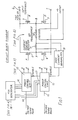
- Fig. 1 is a schematic of the circuitry of a jointless track circuit transmitter
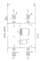
- Fig. 2 shows a bridge of Fig. 1 in more detail
- Fig. 3 is a schematic diagram of a power control unit of Fig. 1;
- Fig. 4 is a schematic diagram of a coded signal generator for the transmitter of Fig. 1;
- Fig. 5 is a wave form diagram for illustrating the operation of the circuitry of Fig. 1.
- a bridge of controllable switching devices 2, 3, 4 and 5 comprising four field-effect transistors, of suitable current capacity, connected in a conventional bridge layout in which a voltage supply source is connected between input terminals 6 and 7 and the output is taken between output terminals 8 and 9 via an output transformer 10 connected between terminals 8 and 9. Also, in series with the primary winding of transformer 10 there is connected a current sensing resistor 11 and in parallel therewith an overcurrent sensing circuit 19 to which further reference will be made below.
- the control gates of the switching devices 2, 3, 4 and 5 are connected so that the devices of each pair of diagonally opposite devices in the bridge are operated by respective control signals from a common one of power control units 12 and 13.
- the power control units 12 and 13 are connected respectively according to the notation shown in Fig. 1.
- the circuits contained within the control units 12 and 13 are identical and each is responsive to two inputs namely a first input 14 or 15 (which is a sensed voltage level derived from the voltage supply connected to bridge input terminals 6 and 7) and a second input 16 or 17 (which operates switching controls in accordance with the desired alternating frequency characteristics required in the final power output appearing across the terminals of the secondary winding of output transformer 10).
- the inputs 16 and 17 are derived from a further block 18 comprising, in the present example, a frequency shift keyed generator.
- the circuit 19 connected in parallel with the current sensing resistor 11 is responsive to the potential difference developed across the resistor 11 by an output current, and the circuit 19 provides alternatively an enable or inhibit output which is connected to provide a third input to the control units 12 and 13, in a manner to be described in further detail with reference to Fig. 3.
- Fig. 2 there is shown an enlarged circuit diagram of the bridge 1.
- the control signals for the switching devices 2, 3, 4 and 5 are supplied from respective control terminals labelled A, B, C and D and via drive stage circuits 21, 22, 23 and 24 respectively to the control gates of the switching devices 2, 3, 4 and 5 respectively.
- the switching devices 2 and 5, which form one diagonal pair of devices, are operated by control signals from the first control unit 12.
- the other diagonal pair of switching devices (3 and 4) are operated by control signals from the second control unit 13.
- the control signals are such that devices 2 and 5 are conductive at the same time for first periods and the devices 3 and 4 are conductive at the same time for second periods, which are out of phase with the first periods.
- circuitry for one form of power control unit suitable for each of units 12 and 13, is illustrated in Fig. 3.
- Other forms of circuit design are suitable.
- the one presently being described employs digital techniques and was selected, inter alia, for the ease with which the operating frequencies can be altered.
- a first, voltage sensing terminal 30 is provided, which is connected externally to a supply voltage sensing point.
- the input terminal 30 is connected via a fixed voltage drop or threshold circuit 31 to the input of an analogue to digital converter 32.
- the supply voltage varies within a voltage output range between limits of, say, 20 and 30 volts, and the minimum voltage which the pulse width modulated circuit can compensate is approximately 18 volts. Therefore, the fixed voltage drop circuit 31 introduces an 18 volt threshold to the input, effectively shifting the range of voltage variation to commence at about zero volts and thereby utilising the analogue to digital converter 32 to the fullest extent possible.
- the converter 32 generates an 8 bit digital representation of a sensed voltage as a parallel output word which is connected to the address input of a programmable read only memory (PROM) 33 which contains a look-up table of digital words or numbers representing the pulse widths indexed against each of the 8 bit words representing a sensed voltage within the operating range.
- PROM 33 programmable read only memory
- the output from the PROM 33 represents the required pulse width by means of an 8 bit digital number.
- the represented pulse width is compensated for the sinusoidal current wave-form of the output in accordance with the formula:
- the PROM output is used as the parallel preset input 34a to a presettable down counter 34.
- This counter 34 is also provided with a clock input 34b which determines the count down rate and a third input 34c which controls the reloading of the 8 bit number at input 34a to reset the counter.
- the final output 34d of the counter comprises a latched output which changes state at the beginning and end of a count period, the counter occupying a first state normally and a second state during the period in which the preset number is being counted downs.
- the counter output 34d is connected to one input of each of two 3-input AND gates 35 and 36, a second input of each of these gates also being connected to a common latched signal line connected to the enable or inhibit output of the overcurrent sensing circuit 19 in Fig. 1.
- the remaining, third input of gate 35 is connected to a frequency signal and the corresponding third input of gate 36 is connected to an inverse of that signal.
- the respective outputs of the gates 35, 36, in Fig. 3 identified as A and D respectively, provide the control signals for the switching devices 2 and 5 of the bridge 1, see Figs. 1 and 2.
- the final output signal is a frequency shift keyed (FSK) power signal and this is generated as a result of the circuit illustrated in Fig. 4.
- An FSK signal comprises a signal which is switched between alternate frequencies at a modulation rate.
- the keyed frequencies are generated by crystal oscillators 40 and 41 which produce upper and lower frequency signals respectively.
- the modulation frequency is generated by a third oscillator 42 and a frequency divider 43.
- the frequency keying at the modulation rate is controlled by a logic gating arrangement generally indicated at 44 and which is of well known configuration.
- the frequency keyed signal produced by the gates 44 is also at a relatively high frequency and is further divided to a lower rate by dividers 45 and 46, the outputs of which are connected to the power control units 12 and 13 (see Fig. 1) respectively.
- the outputs of these dividers provide the clock signal at input 34b of Fig. 3, the FSK signals to gates 35 and 36, and the load signal to input 34c.
- the frequency shift keyed signal is characteristic of the transmitter.
- a track circuit may have one of five alternative nominal carrier frequencies, for example, 4080 Hz, 4560 Hz, 5040 Hz, 5520 Hz and 6000 Hz and the upper and lower keyed frequencies are shifted from these nominal frequencies by 40 Hz.
- each track circuit has a characteristic modulation frequency which may be a constant frequency, or a coded modulation signal, or even an externally variable modulation signal.
- the corresponding FSK signal is generated by the block 18 in Fig. 1, shown in greater detail in Fig. 4. These signals connected to the power control units 12 and 13 in Fig.
- the switching devices 2, 3, 4 and 5 of the bridge 1 cause the switching devices 2, 3, 4 and 5 of the bridge 1 to be operated in order to switch current between the terminals 8 and 9 of the bridge and through the primary winding of transformer 10 to supply the power output through inductive coupling with the secondary of the transformer.
- This current is derived from the voltage supply connected across terminals 6 and 7, which voltage, although normally reasonably stable, may lie within and vary between voltage limits of 20 and 30 volts. It is preferred not to employ a fully stabilised voltage supply because the stabilising electronics of such supplies do not permit of fail-safe characteristics so that some failure modes may result in the production of excessive current and/or voltage.
- An increase in supply voltage to a transmitter without the power control of the embodiment of the present invention, would boost the transmitter output, which is a "wrong side" failure. Therefore, even a stabilised power supply would have to fail safe in the event of a failure occuring the result of which is a supply voltage increase.
- the embodiment of the present invention is preferred and it permits the transmitter to be operated from batteries which
- the variations of the power supply voltage are compensated by variation of the pulse widths of the switching periods of the switching devices 2, 3, 4 and 5 to tend to maintain a constant output power, that is a constant voltage and current product in the transformer primary winding arm of the bridge.
- the instantaneous supply voltage value is sensed by both units 12 and 13 in Fig. 1, one of which is shown in more detail in Fig. 3, and is transformed by the analogue to digital converter 32 and the PROM 33 look-up table to a corresponding pulse width on counter output 34d.
- the result is that the switching control signals at terminals A and D are produced to switch the devices 2 and 5 into a state of conduction for first pulse widths determined in accordance with the given formula.
- the switching control signals at terminals B and C are produced to switch the devices 1 and 3 into a state of conduction for out of phase second pulse widths determined in accordance with the
- the power can only increase up to the limit at which the first and second pulse widths overlap (so that both devices 2 and 4 or both devices 3 and 5 are conductive together) since at that point devices 2 and 4 or devices 3 and 5 will short-circuit the voltage supply and the total current drawn from the voltage supply will exceed the current sensitive rating of the fuse 20 which will then burn out.
- the overcurrent sensing circuit 19 operates in response to a voltage, in excess of a predetermined threshold, developed across the resistor 11 to provide either an enable or inhibit logic output connected to the gates 35 and 36 in the power control units 12 and 13, see Fig. 3. It provides protection against the effects of some faults and, for example, installation errors and effectively protects the fuse 20 from the effects of such faults. Consequently the fuse is rendered responsive only to failures in the power control system itself.
Landscapes
- Engineering & Computer Science (AREA)
- Power Engineering (AREA)
- Inverter Devices (AREA)
- Selective Calling Equipment (AREA)
- Train Traffic Observation, Control, And Security (AREA)
Applications Claiming Priority (2)
| Application Number | Priority Date | Filing Date | Title |
|---|---|---|---|
| GB8419373 | 1984-07-30 | ||
| GB848419373A GB8419373D0 (en) | 1984-07-30 | 1984-07-30 | Power control circuit |
Publications (3)
| Publication Number | Publication Date |
|---|---|
| EP0173445A2 EP0173445A2 (en) | 1986-03-05 |
| EP0173445A3 EP0173445A3 (en) | 1986-10-08 |
| EP0173445B1 true EP0173445B1 (en) | 1991-03-20 |
Family
ID=10564660
Family Applications (1)
| Application Number | Title | Priority Date | Filing Date |
|---|---|---|---|
| EP85305201A Expired - Lifetime EP0173445B1 (en) | 1984-07-30 | 1985-07-22 | Power control circuit |
Country Status (12)
| Country | Link |
|---|---|
| US (1) | US4636933A (da) |
| EP (1) | EP0173445B1 (da) |
| JP (1) | JPS6141668A (da) |
| AU (1) | AU581579B2 (da) |
| BR (1) | BR8503573A (da) |
| CA (1) | CA1250651A (da) |
| DE (1) | DE3582207D1 (da) |
| DK (1) | DK343285A (da) |
| ES (1) | ES8608700A1 (da) |
| GB (1) | GB8419373D0 (da) |
| IN (1) | IN166751B (da) |
| ZA (1) | ZA855372B (da) |
Cited By (1)
| Publication number | Priority date | Publication date | Assignee | Title |
|---|---|---|---|---|
| DE9109503U1 (de) * | 1991-07-31 | 1991-10-17 | Magtron Magneto Elektronische Geraete Gmbh, 7583 Ottersweier | Schaltungsanordnung für ein Stromversorgungsgerät für Geräte und Anlagen der Plasma- und Oberflächentechnik |
Families Citing this family (7)
| Publication number | Priority date | Publication date | Assignee | Title |
|---|---|---|---|---|
| JPH07111918B2 (ja) * | 1987-07-28 | 1995-11-29 | 三菱電機株式会社 | マイクロ波放電光源装置 |
| JP3318240B2 (ja) * | 1997-09-12 | 2002-08-26 | 松下電器産業株式会社 | スイッチング電源装置 |
| ITSV20030022A1 (it) * | 2003-05-22 | 2004-11-23 | Alstom Ferroviaria Spa | Generatore di potenza ad elevata sicurezza intrinseca, in |
| EP2173016A1 (de) * | 2008-10-02 | 2010-04-07 | DBK David + Baader GmbH | Schaltung für einen elektrischen Verbraucher mit einer Lastschaltvorrichtung |
| DE102010000954A1 (de) * | 2010-01-15 | 2011-07-21 | DBK David + Baader GmbH, 76870 | Elektronische Ansteuereinrichtung |
| CN103116241B (zh) * | 2012-11-30 | 2015-03-18 | 华为技术有限公司 | 一种供电电路、芯片和监控设备 |
| CN105245141A (zh) * | 2015-11-16 | 2016-01-13 | 中国电子科技集团公司第四十三研究所 | 一种高压悬浮mosfet/igbt连续栅极驱动电路 |
Family Cites Families (10)
| Publication number | Priority date | Publication date | Assignee | Title |
|---|---|---|---|---|
| GB1504313A (en) * | 1974-03-11 | 1978-03-15 | Nippon Telegraph & Telephone | Inverter controlling device |
| US4099109A (en) * | 1976-10-01 | 1978-07-04 | Westinghouse Electric Corp. | Digital apparatus for synthesizing pulse width modulated waveforms and digital pulse width modulated control system |
| SU720636A1 (ru) * | 1977-10-17 | 1980-03-05 | Московский Ордена Ленина Энергетический Институт | Стабилизированный по напр жению трехфазный мостовой инвертор |
| US4320880A (en) * | 1979-10-17 | 1982-03-23 | General Signal Corp. | Electronic track current switching relay system |
| FR2486329A1 (fr) * | 1980-07-01 | 1982-01-08 | Electronique Vehicules Reseaux | Dispositif de regulation a grande stabilite pour convertisseur d'energie |
| SU964904A1 (ru) * | 1980-08-15 | 1982-10-07 | Опытное Конструкторско-Технологическое Бюро Института Металлофизики Ан Усср | Способ преобразовани и стабилизации переменного напр жени и устройство дл его осуществлени |
| JPS57153569A (en) * | 1981-03-19 | 1982-09-22 | Fuji Electric Co Ltd | Output voltage control system for pulse width modulation inverter |
| JPS5826572A (ja) * | 1981-08-10 | 1983-02-17 | Mitsubishi Electric Corp | 制御装置 |
| DE3131574C2 (de) * | 1981-08-10 | 1987-01-02 | ASR Servotron AG, 1213 Le Petit-Lancy, Genève | "Stromregelschaltung für einen über eine Leistungstreiberstufe gesteuerten Verbraucher" |
| GB2162664B (en) * | 1984-07-30 | 1987-12-16 | Westinghouse Brake & Signal | Power control circuit |
-
1984
- 1984-07-30 GB GB848419373A patent/GB8419373D0/en active Pending
-
1985
- 1985-07-15 IN IN551/DEL/85A patent/IN166751B/en unknown
- 1985-07-16 ZA ZA855372A patent/ZA855372B/xx unknown
- 1985-07-19 US US06/757,219 patent/US4636933A/en not_active Expired - Lifetime
- 1985-07-22 DE DE8585305201T patent/DE3582207D1/de not_active Expired - Fee Related
- 1985-07-22 EP EP85305201A patent/EP0173445B1/en not_active Expired - Lifetime
- 1985-07-23 CA CA000487302A patent/CA1250651A/en not_active Expired
- 1985-07-29 BR BR8503573A patent/BR8503573A/pt unknown
- 1985-07-29 AU AU45567/85A patent/AU581579B2/en not_active Ceased
- 1985-07-29 DK DK343285A patent/DK343285A/da not_active Application Discontinuation
- 1985-07-30 ES ES545713A patent/ES8608700A1/es not_active Expired
- 1985-07-30 JP JP16965285A patent/JPS6141668A/ja active Pending
Cited By (1)
| Publication number | Priority date | Publication date | Assignee | Title |
|---|---|---|---|---|
| DE9109503U1 (de) * | 1991-07-31 | 1991-10-17 | Magtron Magneto Elektronische Geraete Gmbh, 7583 Ottersweier | Schaltungsanordnung für ein Stromversorgungsgerät für Geräte und Anlagen der Plasma- und Oberflächentechnik |
Also Published As
| Publication number | Publication date |
|---|---|
| DK343285D0 (da) | 1985-07-29 |
| ES545713A0 (es) | 1986-06-16 |
| DK343285A (da) | 1986-01-31 |
| EP0173445A3 (en) | 1986-10-08 |
| AU4556785A (en) | 1986-02-06 |
| ZA855372B (en) | 1986-03-26 |
| CA1250651A (en) | 1989-02-28 |
| GB8419373D0 (en) | 1984-09-05 |
| US4636933A (en) | 1987-01-13 |
| DE3582207D1 (de) | 1991-04-25 |
| IN166751B (da) | 1990-07-14 |
| ES8608700A1 (es) | 1986-06-16 |
| EP0173445A2 (en) | 1986-03-05 |
| AU581579B2 (en) | 1989-02-23 |
| BR8503573A (pt) | 1986-04-29 |
| JPS6141668A (ja) | 1986-02-28 |
Similar Documents
| Publication | Publication Date | Title |
|---|---|---|
| EP0173445B1 (en) | Power control circuit | |
| CN1937386A (zh) | 开关式电源中故障检测的方法和装置 | |
| US3697855A (en) | Hysteresis-loop control for a power transformer | |
| US4774925A (en) | Ignition control device | |
| GB2162664A (en) | Power control circuit | |
| US4162442A (en) | Capacitor equipment | |
| US3550006A (en) | Temperature control for crystal oscillator and modulation circuit of a radio transmitter | |
| US3676766A (en) | Multiphase alternating current regulation system for transformer-coupled loads | |
| US4268900A (en) | Device for controlling a plurality of converters | |
| SU851727A1 (ru) | Регул тор переменного напр жени диСКРЕТНОгО дЕйСТВи | |
| EP0218414A3 (en) | Static inverter | |
| EP0083866A2 (en) | An A.C. supply converter | |
| SU1156030A1 (ru) | Стабилизатор переменного напр жени | |
| SU1656631A1 (ru) | Система электроснабжени | |
| SU1097985A1 (ru) | Стабилизатор переменного напр жени | |
| SU941966A1 (ru) | Стабилизатор посто нного напр жени | |
| SU1197025A1 (ru) | Стабилизирующий источник вторичного электропитани | |
| US3448294A (en) | Multiphase power switching circuit | |
| SU1064403A1 (ru) | Преобразователь посто нного напр жени в переменное | |
| US3950692A (en) | Method and device for d.c. voltage regulation across load | |
| SU743138A1 (ru) | Регулируемый преобразователь напр жени | |
| SU1591088A1 (ru) | Бесконтактное устройство для регулирования напряжения трехфазного силового трансформатора | |
| SU1300620A2 (ru) | Статический преобразователь дл питани гистерезисного двигател | |
| SU957411A1 (ru) | Устройство дл управлени многофазным импульсным регул тором | |
| SU851382A1 (ru) | Устройство дл регулировани выпр млен-НОгО НАпР жЕНи |
Legal Events
| Date | Code | Title | Description |
|---|---|---|---|
| PUAI | Public reference made under article 153(3) epc to a published international application that has entered the european phase |
Free format text: ORIGINAL CODE: 0009012 |
|
| AK | Designated contracting states |
Kind code of ref document: A2 Designated state(s): CH DE FR IT LI NL SE |
|
| PUAL | Search report despatched |
Free format text: ORIGINAL CODE: 0009013 |
|
| AK | Designated contracting states |
Kind code of ref document: A3 Designated state(s): CH DE FR IT LI NL SE |
|
| 17P | Request for examination filed |
Effective date: 19870403 |
|
| 17Q | First examination report despatched |
Effective date: 19881229 |
|
| RAP1 | Party data changed (applicant data changed or rights of an application transferred) |
Owner name: WESTINGHOUSE BRAKE AND SIGNAL HOLDINGS LIMITED |
|
| GRAA | (expected) grant |
Free format text: ORIGINAL CODE: 0009210 |
|
| AK | Designated contracting states |
Kind code of ref document: B1 Designated state(s): CH DE FR IT LI NL SE |
|
| PG25 | Lapsed in a contracting state [announced via postgrant information from national office to epo] |
Ref country code: SE Effective date: 19910320 Ref country code: NL Effective date: 19910320 Ref country code: IT Free format text: LAPSE BECAUSE OF FAILURE TO SUBMIT A TRANSLATION OF THE DESCRIPTION OR TO PAY THE FEE WITHIN THE PRESCRIBED TIME-LIMIT;WARNING: LAPSES OF ITALIAN PATENTS WITH EFFECTIVE DATE BEFORE 2007 MAY HAVE OCCURRED AT ANY TIME BEFORE 2007. THE CORRECT EFFECTIVE DATE MAY BE DIFFERENT FROM THE ONE RECORDED. Effective date: 19910320 Ref country code: FR Effective date: 19910320 |
|
| REF | Corresponds to: |
Ref document number: 3582207 Country of ref document: DE Date of ref document: 19910425 |
|
| PG25 | Lapsed in a contracting state [announced via postgrant information from national office to epo] |
Ref country code: LI Effective date: 19910731 Ref country code: CH Effective date: 19910731 |
|
| EN | Fr: translation not filed | ||
| NLV1 | Nl: lapsed or annulled due to failure to fulfill the requirements of art. 29p and 29m of the patents act | ||
| PLBE | No opposition filed within time limit |
Free format text: ORIGINAL CODE: 0009261 |
|
| STAA | Information on the status of an ep patent application or granted ep patent |
Free format text: STATUS: NO OPPOSITION FILED WITHIN TIME LIMIT |
|
| 26N | No opposition filed | ||
| REG | Reference to a national code |
Ref country code: CH Ref legal event code: PL |
|
| PGFP | Annual fee paid to national office [announced via postgrant information from national office to epo] |
Ref country code: DE Payment date: 19920903 Year of fee payment: 8 |
|
| PG25 | Lapsed in a contracting state [announced via postgrant information from national office to epo] |
Ref country code: DE Effective date: 19940401 |