EP0172679A1 - Frequenzmodulation- und Demodulation - Google Patents
Frequenzmodulation- und Demodulation Download PDFInfo
- Publication number
- EP0172679A1 EP0172679A1 EP85305350A EP85305350A EP0172679A1 EP 0172679 A1 EP0172679 A1 EP 0172679A1 EP 85305350 A EP85305350 A EP 85305350A EP 85305350 A EP85305350 A EP 85305350A EP 0172679 A1 EP0172679 A1 EP 0172679A1
- Authority
- EP
- European Patent Office
- Prior art keywords
- frequency
- signal
- direct current
- voltage
- demodulated
- Prior art date
- Legal status (The legal status is an assumption and is not a legal conclusion. Google has not performed a legal analysis and makes no representation as to the accuracy of the status listed.)
- Withdrawn
Links
Images

Classifications
-
- H—ELECTRICITY
- H03—ELECTRONIC CIRCUITRY
- H03C—MODULATION
- H03C3/00—Angle modulation
-
- H—ELECTRICITY
- H03—ELECTRONIC CIRCUITRY
- H03D—DEMODULATION OR TRANSFERENCE OF MODULATION FROM ONE CARRIER TO ANOTHER
- H03D3/00—Demodulation of angle-, frequency- or phase- modulated oscillations
Definitions
- the present invention relates to frequency modulation and demodulation.
- the present invention relates to frequency modulation and demodulation using materials that carry a sliding charge density wave.
- the fundamental purpose of modulation is to superimpose the desired intelligence signals on a high-frequency carrier for transmission at that high frequency fran one point to another.
- a signal is transmitted from one point to another for a variety of purposes.
- the most common example is communications between geographic areas.
- a communications e.g., telephone
- the physical equipment usually involves an enormous quantity of hardware (e.g., poles, cross-arms, insulators, and wires).
- hardware e.g., poles, cross-arms, insulators, and wires.
- One method of increasing the facility of a circuit is to use a method of modulation.
- a voice-frequency band from 200 to 3000 cycles is required for telephone conmunications. If we take bands of frequencies, 0 to 3 kc, 3 to 6 kc, 6 to 9 kc, 9 to 12 kc, and 12 to 15 kc a total band of 0 to 15 kc apparently could provide five separate channels for five separate telephone circuits over one pair of wires, provided that the original band of 200 to 3000 cycles can be transferred to each of the high-frequency bands.
- modulation The process of superimposing the information contained within a frequency band onto another frequency band.
- decoding or converting the signal back to its original form is called demodulation or detection.
- the energy medium by which the signal is to be transferred is called the carrier.
- the signal is often termed the modulating frequency. If we consider a single-frequency carrier, ⁇ o , we may write
- Frequency modulation is superior to amplitude modulation for reducing the static and noise present in home reception of the standard AM broadcasts. Since most natural and manmade electrical noise is in the form of amplitude-modulated signals, a method of keeping the amplitude E m constant while incorporating the signal into variations of the carrier frequency ⁇ o accomplishes the desired noise reduction.
- the frequency ⁇ o is modified by the signal amplitude and signal frequency.
- the deviation frequency, ⁇ f from ⁇ o contains the information on the amplitude or volume of the signal.
- the frequency of the signal, ⁇ m is the rate of change of the output frequency.
- the FM output wave can be written as an infinite series of terms (carrier plus sidebands) containing Bessel functions which depend on m r and ⁇ m .
- CDW Charge Density Waves
- charge transport is usually field and frequency-dependent at moderate fields and frequencies in materials where the electron structure, and consequently the conduction process, is highly anisotropic.
- Low dimensional conductors or linear chain conductors are materials which have a chain structure: the solid is built of chains of atoms or molecules with strongly overlapping electronic wave functions along the chain direction, while the coupling or overlap of the wave functions between the chains is weak. This chain structure leads therefore to highly anisotropic electronic band structures.
- Drastic deviations from single particle transport are expected in linear chain compounds.
- collective modes appear where a periodic modulation of the charge density occurs.
- the CDW is pinned by the impurities present in the sample in the absence of a driving electric field.
- a d.c. electric field above a certain threshold value is applied to the sample, the CDW is depinned and is able to slide through the sample, thereby providing a new mechanism of charge transport.
- the sliding CDW is associated with the onset of a non-linear current-voltage characteristic and the appearance of an a.c. component in the current.
- the fundamental component of the a.c. current is found to be proportional to the excess current that is carried by the CDW.
- This a.c. component is known as the narrow-band-noise or the coherent current oscillations.
- the frequency spectrum of this a.c. component consists of well-defined peaks at the fundamental and its higher harmonics.
- these characteristics of the sliding of the CDW are utilized in a method and system for the frequency modulation of a carrier frequency by a signal frequency.
- the invention also relates to the converse situation, i.e. frequency demodulation.
- a method for frequency modulating a signal comprising:
- a method for frequency demodulating a signal comprising:
- a device for frequency modulation of a signal comprising:
- a device for frequency demodulation of a signal comprising:
- the description which follows relates to a system and method for frequency modulation or frequency demodulation of a signal.
- a carrier-frequency which is tunable, is generated.
- a modulation frequency then modulates the carrier.
- the system for the modulation of the carrier depends on the effect of a.c. - d.c. mixing in the sliding CDW which is caused by driving the system with an amplitude-modulated field. This field generates frequency modulated coherent current oscillations.
- the frequency spectrum of the current of one preferred embodiment, orthorhanbic TaS 3 develops side-bands at frequencies ⁇ o + n ⁇ m where ⁇ o is the material fundamental of the current oscillation in the absence of the a.c. modulation. Varying the amplitude of the modulation results in the variation of the amplitude of the side-bands and the carrier frequency. This variation is found to be in excellent agreement with the results obtained theoretically for the general case of frequency modulation (FM) with no adjustable parameters.
- FM frequency modulation
- the sliding CDW system acts as a single crystal frequency modulator.
- a decided advantage of the CDW system lies in the tunability of the carrier-frequency (1kHz - 1GHz).
- the sliding charge density wave (CDW) conductors display intriguing electrical transport properties such as the non-linear conductivity and the coherent current oscillations - the so-called narrow-band-noise when a d.c. electric field above a certain threshold value is applied to the sample.
- the frequency of the oscillations is found to scale linearly with the non-linear part of the d.c. current.
- the voltage as a function of frequency is:
- Eq.3 is the standard expression for frequency modulation. A comparison with experimental results measures the quality of the performance of the device.
- a single crystal of orthorhombic TaS 3 , 2 was mounted in a configuration shown schematically in Figure 1 and maintained at 130°K where it is in its CDW state.
- a d.c. voltage in excess of the threshold field was established. With only the d.c. of 60 mV across the sample the characteristic a.c. signal appeared at 830 kHz.
- the d.c. voltage, applied by variable d.c. voltage source 4, and a.c. signal voltage 6 are both applied to the crystal 2.
- the resulting frequency modulated signal, V OUT is then obtained from the material 2.
- TaS 3 is employed as a material that displays the CDW state.
- any material that displays the CDW state may be used.
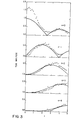
- On superimposing an a.c. voltage at a frequency of 50 kHz sidebands of the 830 kHz signal appeared which were multiples of 50 kHz to the high and low sides of the fundamental peak.
- the amplitude of the a.c. is increased the magnitude and number of sidebands increase.
- Typical spectra for three values of the a.c. amplitude are shown in Figure 2.
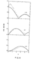
- the frequency ⁇ M of the modulating signal was varied.
- the modulation frequency was 100 kHz.
- the fit up to the third sideband is again excellent, with the systematic background problem evident again for the fundamental.
- This example shows the performance of the material orthorhombic TaS 3 as a single crystal frequency modulator. It is noted that the same system in Figure 1 will also act as a demodulator. In this case, a variable direct current voltage 4 is applied so that the a.c. frequency equals the carrier frequency of the signal to be demodulated. Then the signal to be demodulated 6 is applied in series with the d.c. voltage. The resulting frequency demodulated signal, V OUT , is then obtained from the material 2 whose amplitude and frequency spectrum varies in a predetermined way that depends on the amplitude of the carrier signal generated by the direct current voltage applied to the system. Since the basis of the operation of the system is caused by the presence of a sliding charge density wave, all materials which have such a state will also act as frequency modulators, or demodulators.
Landscapes
- Engineering & Computer Science (AREA)
- Power Engineering (AREA)
- Amplitude Modulation (AREA)
- Channel Selection Circuits, Automatic Tuning Circuits (AREA)
- Transmitters (AREA)
- Circuits Of Receivers In General (AREA)
Applications Claiming Priority (2)
| Application Number | Priority Date | Filing Date | Title |
|---|---|---|---|
| US06/634,823 US4580110A (en) | 1984-07-26 | 1984-07-26 | Frequency modulator using material having sliding charge density waves |
| US634823 | 1984-07-26 |
Publications (1)
| Publication Number | Publication Date |
|---|---|
| EP0172679A1 true EP0172679A1 (de) | 1986-02-26 |
Family
ID=24545320
Family Applications (1)
| Application Number | Title | Priority Date | Filing Date |
|---|---|---|---|
| EP85305350A Withdrawn EP0172679A1 (de) | 1984-07-26 | 1985-07-26 | Frequenzmodulation- und Demodulation |
Country Status (4)
| Country | Link |
|---|---|
| US (1) | US4580110A (de) |
| EP (1) | EP0172679A1 (de) |
| JP (1) | JPS6141209A (de) |
| CA (1) | CA1244102A (de) |
Families Citing this family (6)
| Publication number | Priority date | Publication date | Assignee | Title |
|---|---|---|---|---|
| GB2256314B (en) * | 1991-01-25 | 1994-09-07 | Hitachi Europ Ltd | Charge density wave semiconductor device |
| US6735073B2 (en) | 2002-01-09 | 2004-05-11 | Lucent Technologies Inc. | Electronic devices based on density wave dielectrics |
| US7700006B2 (en) * | 2002-05-31 | 2010-04-20 | Alcatel-Lucent Usa Inc. | Voltage regulators |
| US6724056B1 (en) | 2003-04-15 | 2004-04-20 | Lucent Technologies Inc. | Field-effect transistors with high-sensitivity gates |
| US7645850B2 (en) * | 2005-08-11 | 2010-01-12 | Frx Polymers, Inc. | Poly(block-phosphonato-ester) and poly(block-phosphonato-carbonate) and methods of making same |
| CN104981474A (zh) | 2013-01-22 | 2015-10-14 | Frx聚合物股份有限公司 | 含磷环氧化合物及其组合物 |
Citations (1)
| Publication number | Priority date | Publication date | Assignee | Title |
|---|---|---|---|---|
| US3042853A (en) * | 1957-06-24 | 1962-07-03 | Rca Corp | Semiconductor electrical apparatus |
Family Cites Families (1)
| Publication number | Priority date | Publication date | Assignee | Title |
|---|---|---|---|---|
| US3818377A (en) * | 1969-09-19 | 1974-06-18 | Matsushita Electric Industrial Co Ltd | Oscillatory device utilizing pulse generating diode |
-
1984
- 1984-07-26 US US06/634,823 patent/US4580110A/en not_active Expired - Fee Related
-
1985
- 1985-07-25 CA CA000487475A patent/CA1244102A/en not_active Expired
- 1985-07-26 EP EP85305350A patent/EP0172679A1/de not_active Withdrawn
- 1985-07-26 JP JP16564685A patent/JPS6141209A/ja active Pending
Patent Citations (1)
| Publication number | Priority date | Publication date | Assignee | Title |
|---|---|---|---|---|
| US3042853A (en) * | 1957-06-24 | 1962-07-03 | Rca Corp | Semiconductor electrical apparatus |
Non-Patent Citations (1)
| Title |
|---|
| PATENT ABSTRACTS OF JAPAN, vol. 8, no. 243 (E-277)[1680], 8th November 1984; & JP - A - 59 122 002 (TOSHIBA K.K.) 14-07-1984 * |
Also Published As
| Publication number | Publication date |
|---|---|
| JPS6141209A (ja) | 1986-02-27 |
| US4580110A (en) | 1986-04-01 |
| CA1244102A (en) | 1988-11-01 |
Similar Documents
| Publication | Publication Date | Title |
|---|---|---|
| US2283575A (en) | High frequency transmission system | |
| DE2304352A1 (de) | Schaltungsanordnung zum verstaerken eines eingangssignals | |
| EP0172679A1 (de) | Frequenzmodulation- und Demodulation | |
| US4636737A (en) | Frequency modulator and demodulator using material having sliding charge density waves | |
| KR840008095A (ko) | 대중 대역동조 시스템 | |
| US2420892A (en) | Frequency modulation detector | |
| US3286024A (en) | Non-linear video-signal modulating systems with a characteristic "instantaneous frequency deviation vs. pre-emphasized signal level" having a decreasing slope with increasing absolute value of signal level | |
| US3479607A (en) | Frequency discriminator with injection-locked oscillator | |
| EP0511989B1 (de) | Amplitudenregelkreisschaltungen | |
| Townes et al. | Stark effect in high frequency fields | |
| CN108092932A (zh) | 一种基于双边带调制器和倍频器非线性效应的频率可调多频率输出微波源 | |
| Gardiner et al. | Distortion performance of single-balanced diode modulators | |
| US4902987A (en) | Inductive modulator system | |
| US2045796A (en) | Method for radio transmission | |
| US1699570A (en) | Carrier suppression modulation | |
| US3440569A (en) | Noise reduction in frequency modulation system | |
| EP0720315A1 (de) | Verfahren zur schmallbandigen Frequenz- oder Phasenmodulation Sender und Empfänger zur Ausführung des Verfahrens | |
| CN207819962U (zh) | 一种频率可调多频率输出微波源 | |
| US3373381A (en) | Transmission line phase modulator | |
| Chramiec | Subharmonically pumped Schottky diode single sideband modulator | |
| US3183447A (en) | Voltage-controlled nondispersive variable delay system utilizing modulation to pass signal and frequencyinverted signal through identical dispersive delay lines | |
| SU862354A1 (ru) | Генератор линейно-частотно-модулированных сигналов | |
| Howson et al. | High-frequency mixers using square-law diodes | |
| SU809600A1 (ru) | Устройство дл компенсации помехпРи пРиЕМЕ фАзОМОдулиРОВАННыХСигНАлОВ | |
| Brabham | Spectra in angle-modulated waves |
Legal Events
| Date | Code | Title | Description |
|---|---|---|---|
| PUAI | Public reference made under article 153(3) epc to a published international application that has entered the european phase |
Free format text: ORIGINAL CODE: 0009012 |
|
| AK | Designated contracting states |
Designated state(s): DE FR GB |
|
| 17P | Request for examination filed |
Effective date: 19860723 |
|
| STAA | Information on the status of an ep patent application or granted ep patent |
Free format text: STATUS: THE APPLICATION HAS BEEN WITHDRAWN |
|
| 18W | Application withdrawn |
Withdrawal date: 19870512 |
|
| RIN1 | Information on inventor provided before grant (corrected) |
Inventor name: STOKES, JAMES PETER Inventor name: BLOCH, AARON NIXON Inventor name: BHATTACHARYA, SABYASACHI |