EP0172112B1 - Semiconductor memory device - Google Patents
Semiconductor memory device Download PDFInfo
- Publication number
- EP0172112B1 EP0172112B1 EP85401626A EP85401626A EP0172112B1 EP 0172112 B1 EP0172112 B1 EP 0172112B1 EP 85401626 A EP85401626 A EP 85401626A EP 85401626 A EP85401626 A EP 85401626A EP 0172112 B1 EP0172112 B1 EP 0172112B1
- Authority
- EP
- European Patent Office
- Prior art keywords
- data
- word
- memory device
- transistor
- bit
- Prior art date
- Legal status (The legal status is an assumption and is not a legal conclusion. Google has not performed a legal analysis and makes no representation as to the accuracy of the status listed.)
- Expired - Lifetime
Links
- 239000004065 semiconductor Substances 0.000 title claims description 20
- 230000000295 complement effect Effects 0.000 claims description 20
- 230000004044 response Effects 0.000 claims description 10
- 239000003990 capacitor Substances 0.000 claims description 7
- 238000010276 construction Methods 0.000 description 6
- 238000010586 diagram Methods 0.000 description 4
- 238000003491 array Methods 0.000 description 2
- 238000007796 conventional method Methods 0.000 description 1
- 230000000694 effects Effects 0.000 description 1
- 238000000034 method Methods 0.000 description 1
- 238000012986 modification Methods 0.000 description 1
- 230000004048 modification Effects 0.000 description 1
Images


Classifications
-
- G—PHYSICS
- G11—INFORMATION STORAGE
- G11C—STATIC STORES
- G11C11/00—Digital stores characterised by the use of particular electric or magnetic storage elements; Storage elements therefor
- G11C11/21—Digital stores characterised by the use of particular electric or magnetic storage elements; Storage elements therefor using electric elements
- G11C11/34—Digital stores characterised by the use of particular electric or magnetic storage elements; Storage elements therefor using electric elements using semiconductor devices
- G11C11/40—Digital stores characterised by the use of particular electric or magnetic storage elements; Storage elements therefor using electric elements using semiconductor devices using transistors
-
- G—PHYSICS
- G11—INFORMATION STORAGE
- G11C—STATIC STORES
- G11C7/00—Arrangements for writing information into, or reading information out from, a digital store
-
- G—PHYSICS
- G11—INFORMATION STORAGE
- G11C—STATIC STORES
- G11C11/00—Digital stores characterised by the use of particular electric or magnetic storage elements; Storage elements therefor
- G11C11/21—Digital stores characterised by the use of particular electric or magnetic storage elements; Storage elements therefor using electric elements
- G11C11/34—Digital stores characterised by the use of particular electric or magnetic storage elements; Storage elements therefor using electric elements using semiconductor devices
- G11C11/40—Digital stores characterised by the use of particular electric or magnetic storage elements; Storage elements therefor using electric elements using semiconductor devices using transistors
- G11C11/401—Digital stores characterised by the use of particular electric or magnetic storage elements; Storage elements therefor using electric elements using semiconductor devices using transistors forming cells needing refreshing or charge regeneration, i.e. dynamic cells
- G11C11/4063—Auxiliary circuits, e.g. for addressing, decoding, driving, writing, sensing or timing
- G11C11/407—Auxiliary circuits, e.g. for addressing, decoding, driving, writing, sensing or timing for memory cells of the field-effect type
- G11C11/409—Read-write [R-W] circuits
- G11C11/4094—Bit-line management or control circuits
-
- G—PHYSICS
- G11—INFORMATION STORAGE
- G11C—STATIC STORES
- G11C11/00—Digital stores characterised by the use of particular electric or magnetic storage elements; Storage elements therefor
- G11C11/21—Digital stores characterised by the use of particular electric or magnetic storage elements; Storage elements therefor using electric elements
- G11C11/34—Digital stores characterised by the use of particular electric or magnetic storage elements; Storage elements therefor using electric elements using semiconductor devices
- G11C11/40—Digital stores characterised by the use of particular electric or magnetic storage elements; Storage elements therefor using electric elements using semiconductor devices using transistors
- G11C11/401—Digital stores characterised by the use of particular electric or magnetic storage elements; Storage elements therefor using electric elements using semiconductor devices using transistors forming cells needing refreshing or charge regeneration, i.e. dynamic cells
- G11C11/4063—Auxiliary circuits, e.g. for addressing, decoding, driving, writing, sensing or timing
- G11C11/407—Auxiliary circuits, e.g. for addressing, decoding, driving, writing, sensing or timing for memory cells of the field-effect type
- G11C11/409—Read-write [R-W] circuits
- G11C11/4096—Input/output [I/O] data management or control circuits, e.g. reading or writing circuits, I/O drivers or bit-line switches
-
- G—PHYSICS
- G11—INFORMATION STORAGE
- G11C—STATIC STORES
- G11C7/00—Arrangements for writing information into, or reading information out from, a digital store
- G11C7/20—Memory cell initialisation circuits, e.g. when powering up or down, memory clear, latent image memory
Definitions
- the present invention relates to a semiconductor memory device. More particularly, it relates to a dynamic random access memory provided with a means for clearing the stored data of all bits at the same time.
- the memory devices are those used in, for example, a graphic display system or when an initialization is carried out in a computer system, the data stored in memory devices must be quickly cleared as the same time.
- the memory cells on one side of the memory cell arrays with respect to sense amplifiers represent discharged states
- the memory cells on the other side of the memory cell arrays with respect to sense amplifiers represent charged states. That is, for the same input/output data, the one half of the memory cells do not store charges while the other half of the memory cells do store charges, and vice versa. In other words, the charging states of the memory cells for the same input/output data are different. Therefore, to clear all bits of the memory cells, that is, to input the same data "0" into all of the memory cells, one half of the memory cells should be discharged and the other half of the memory cells should be charged.
- an object of the present invention is in a semiconductor memory device, to clear the memory cells of all bits at substantially the same time and with a small power consumption by employing a very simple circuit.
- a semiconductor memory device comprising a plurality of bit-line pairs, a plurality of memory cells connected to bit lines constituting respective bit line pairs, a plurality of sense amplifiers each provided to correspond to one bit-line pair and each having a pair of complementary signal terminals connected to the bit lines of the corresponding bit-line pair, a pair of data buses for inputting and outputting data to and from a selected bit-line pair, characterized by further comprising a data inverting circuit, operatively connected to the pair of data buses for selectively inverting an input/ output data in such a way that the charging states of respective memory cells connected to the two bit lines of each bit-line pair become equal for the same input/output data, and a clamp circuit for drawing the potentials of all of the bit lines to a predetermined potential in response to a clear control signal applied when the contents of all of said memory cells are to be cleared.
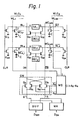
- Figure 1 shows a dynamic random access memory as a semiconductor memory device according to an embodiment of the present invention.
- the memory device in the figure is constructed basically by sense amplifiers SA I , SA 2 , ..., bit lines BL,, BL 1 , BL 2 , BL 2 , ..., connected to complementary input/output terminals a and b of these respective sense amplifiers SA 1 , SA 2 , ..., word lines WL 1 , ..., WL ss , ..., and memory cells MC 1 , 1 , ... , MC 1,65 ... , MC 2,1, ⁇ , MC2,65, ..., arranged at the intersecting portions of the respective bit lines and word lines.
- Each memory cell is constructed by one MIS transistor T and a capacitor C.
- the gate and the source (or drain) of the MIS transistor T are respectively connected to the corresponding word line and to the bit line.
- a pair of data buses DB and DB is arranged at both sides of the respective sense amplifiers SA 1 , SA 2 ,
- One of the word lines WL,, ..., WL ss , ..., and WL 128 is selected by a word decoder WD in response to address signals A o through A 6 .
- the output buffer circuit BUF has two inputs, for receiving complementary signals, connected to nodes g and h respectively.
- the output buffer circuit BUF provides an output data D out of "1" when the input connected to the node g is at the high level and the input connected to the node h is at the low level.
- the output buffer circuit BUF provides an output data D out of "0" when the inputs connected to the nodes g and h are at the low level and at the high level, respectively.
- the write-in amplifier WA has two outputs, for providing complementary signals, connected to the nodes g and h respectively.
- the input data D 1N is "1”
- the output connected to the node g becomes high level and the output connected to the node h becomes low level.
- the input data D IN is "0”
- the output connected to the node g becomes low level and the output connected to the node h becomes high level.
- the transistors Q a and Q b are connected respectively between the data bus DB and the node g and between the data bus DB and the node h.
- the transistors Q c and Q d are connected respectively between the data bus DB and the node g and between the data bus DB and the node h.
- Each of these transistors Q a , Q b , Q c , and Q d is controlled by a pair of complementary signals A 6 and As output from the word decoder WD.
- the transistors Q a and Q b are simultaneously turned ON or OFF by, for example, a signal A 6 which is an inverted signal of the most-significant bit address signal A 6 for selecting a word line.
- the transistors Q c and Q d are simultaneously turned ON or OFF by the address signal A 6 .
- the data buses DB and DB are connected to the nodes g and h in a straight connection.
- the transistors Q a and Q b are OFF and the transistors Q c and Q d are ON, the data buses DB and DB are connected to the nodes h and g in a cross connection.
- clamping transistors Q 13 , Q 14 , Q 23 , Q 24 , ... are connected between respective bit lines BL 1 , BL 1 , BL 2 , BL 2 , ..., and the ground.
- a clear signal CLR is applied to the gates of these transistors Q 13 , Q 14 , Q 23 , Q 24 , ⁇ ⁇ ⁇
- a word line for example, WL 1
- the word decoder WD which receives address signals A o through A 6 , so that all the memory cells MC 1,1 , MC 2,1 , ..., connected to the word line WL, are turned ON.
- the output of one column decoder, for example, DEC 1 is raised to a high level by a column address signal so that the transistors Q 11 and Q 12 are both turned ON and the bit lines BL 1 and BL 1 are respectively connected through the transistors Q 11 and Q 12 to the data buses DB and DB.
- the switch circuit SW receives the most-significant bit address signal A 6 and forms the address signal A 6 and its inverted signal A 6 which are applied respectively to the gates of the transistors Q a , Q b and Q c , Q d .
- the address signal A 6 is at a low level, that is "0”
- the inverted address signal A 6 becomes high level so that the transistors Q a and Q b are turned ON.
- an input data D IN is changed through the write-in amplifier WA to complementary signals.
- the complementary signals are input through the transistors Q a and Q b to the data buses DB and DB.
- the complementary write-in signals input to the data buses DB and DB are transferred through the transistors Q 11 and Q 12 to the bit lines BL, and BL 1 .
- the input data D lN is, for example, "1”
- the data bus DB and, accordingly, the bit line BL 1 become high level, so that positive charges are stored in the capacitor C of the memory cell MC 1,1 , connected to the word line WL, and the bit line BL 1 , and thus, data "1" is stored.
- the charging state of the memory cell MC 1,1 for the input data "1" is the charged state. Note that, in Fig.
- one word line for example, WL 1
- an output of one column decoder for example, DEC 1
- DEC 1 an output of one column decoder
- the transistors Q 11 and Q 12 are turned ON to connect the bit lines BL, and BL 1 , with the data buses DB and DB.
- SA 1 the output of the sense-amplifier SA 1 is obtained on the data buses DB and DB.
- the transistors Q a and Q b are turned ON in response to the high level of the inverted signal A 6 , the potentials of the data buses DB and DB are input through these transistors to the output buffer BUF and a read data D out is output.
- the read data D out is "1". Conversely, if the selected memory cell MC 1,1 , was not storing a charge, the read data D out is "0".
- a word line for example, WL 65 is selected and the potential difference between the bit lines BL 1 and BL 1 , generated in accordance with .the storing state of the memory cell MC 1,65 connected to the word line WL 65 and the bit line BL 1 , is amplified by the sense amplifier SA 1 and is output to the data buses DB and DB.
- the transistors Q c and Q d are turned ON in response to the address signal As of "1"
- the signals on the data buses DB and DB are input, with their reversed phases, to the output buffer BUF. Therefore, as the read out data D out , the reversed-phase data output is output.
- the same read out data D out can be obtained when the charging states of the memory cells arranged on both sides of the sense amplifiers SA 1 , SA 2 , ..., are the same.
- the data bus DB becomes low level and the data bus DB becomes high level.
- This high and low level relationship of the data buses DB and DB is different from that when the memory cell MC 1,1 , which is storing charges, is selected. Nevertheless, through the transistors Q c and Q d , the node g becomes high level and the node h becomes low level. Therefore, when the selected memory cell MC 1,65 was storing charges, the read data D out is "1".
- the clamping transistors Q 13 , Q 14 , Q 23 , Q 24 , ..., connected to all of the bit lines are turned ON by applying a clear signal CLR to the gates of all clamping transistors, to cause the bit line potentials to become 0 volt.
- all the word lines may be selected sequentially by scanning the word address so that transfer gate transistors T along each word line WL 1 , ..., WL 65 , ..., turn on successively and discharge the associated capacitors C.
- all of the word lines may be selected to raise the voltages of all of the word lines WL,, ..., WL 65 simultaneously, ..., to be higher than the threshold voltage Vth of the transfer gate transistor T of each memory cell.
- This causes all of the charges stored in the capacitors of the respective memory cells MC to be discharged through the respective bit lines and the clamping transistors Q 13 , Q 14 , Q 23 , Q 24 , ..., at a time.
- the operation for clearing all of the memory cells MC is carried out.
- Figure 2 shows an example of the word decoder WD used in the above-mentioned memory device.
- the word decoder in the figure has an address buffer unit WAB which includes a plurality of address buffer circuits AB o , AB 1 , AB 2 , . , for forming inverted and non-inverted signals of the respective address signals A o , A 1 , A 2 , ..., and A 6 , and NOR gates N 1 , N 2 , N 3 , ..., and N 128 to which respective outputs of said address buffer unit WAB are selectively input. That is, each NOR gate N i receives 6 bits of a selected combination of the address signals A 1 through A 6 and A 1 through A 6 .
- Figure 3 shows the address buffer circuit AB i , for one bit.
- the address buffer circuit in the figure comprises inverters INV 1 and INV 2 , transistors Q 31 , Q 32 , Q 33 , Q 34 , Q 35 , and Q 36 , and a clock signal generator CLK.
- a reset signal ⁇ R need be applied to the gates of the transistors Q 35 and Q 36 during a reset interval and the generation of a clock pulse ⁇ A , which is usually applied from the clock signal generator CLK to the drains of the transistors Q 31 and Q 32 during an address selection (active interval) is prohibited by applying a stop signal ST to the clock signal generator CLK.
- Figure 4 shows an example of the construction of each of the NOR gates N 1 , N 2 , ..., shown in Fig. 2.
- the NOR gate N shown in Fig. 4 comprises transistors Q 40 , Q 41 , ..., and Q 4N connected in parallel, a reset transistor Q R , a transfer gate transistor Q S , and an output transistor Q T .
- a clock signal ⁇ A may be applied. During a usual read/ write operation, the clock signal ⁇ A is made to the high level.
- the clock signal ⁇ A is made to be high level during a reset interval so as to make a node M 2 between the drain (source) of the transistor Q s and the gate of the transistor Q T to be high level, and then, before starting the operation of the NOR gates, that is, before applying the address signals A o (A o ) through As (A 6 ) to the NOR gates N 1 through N 128 , the clock signal ⁇ A is made low level so that the transistor Q s is turned OFF and, therefore, the node M 2 is maintained at the high level state even after the node M 1 is turned to the low level.
- the output transistor Q T in each NOR gate N is kept ON, resulting in attaining the all selection state.
- the present invention in a dynamic random access memory, by adding a simple circuit including the clamping transistors and the inverting circuit, an operation for clearing all of the bits can be carried out surely and at substantially the same time. Also, in the clearing operation, since it is sufficient to raise the voltages of the word lines to be higher than the threshold voltage of the transfer gate transistor T in each memory cell, it is not necessary to enlarge the driving capability for the word-decoder output for the clearing operation, and thus the clearing operation can be effected at a high speed. Further, the power consumption during the clear operation can be made relatively small.
- the present invention is not restricted to the above-described embodiment of the present invention.
- Various changes and modifications are possible without departing from the scope of the present invention.
- the present invention is applicable to a memory device having a so-called folded bit line construction as disclosed in U.S. Patent 4,025,907 in which each pair of bit lines are extending on one side of the associated sense amplifier in contrast to the open bit line construction of the above-described embodiment.
Landscapes
- Engineering & Computer Science (AREA)
- Microelectronics & Electronic Packaging (AREA)
- Computer Hardware Design (AREA)
- Databases & Information Systems (AREA)
- Dram (AREA)
Description
- The present invention relates to a semiconductor memory device. More particularly, it relates to a dynamic random access memory provided with a means for clearing the stored data of all bits at the same time.
- In general, when the memory devices are those used in, for example, a graphic display system or when an initialization is carried out in a computer system, the data stored in memory devices must be quickly cleared as the same time.
- Conventionally, in a dynamic random access memory, when the memory cells of all bits are to be cleared, data "0" is written by sequentially specifying addresses for respective memory cells.
- However, such a conventional technique is disadvantageous in that a long time is necessary for clearing all the bits and that a special circuit device or a program is necessary for providing the addresses of the memory cells to be sequentially cleared to the memory device.
- From another point of view, in a conventional dynamic random access memory, for the same input/output data, for example, "0", the memory cells on one side of the memory cell arrays with respect to sense amplifiers represent discharged states, and the memory cells on the other side of the memory cell arrays with respect to sense amplifiers represent charged states. That is, for the same input/output data, the one half of the memory cells do not store charges while the other half of the memory cells do store charges, and vice versa. In other words, the charging states of the memory cells for the same input/output data are different. Therefore, to clear all bits of the memory cells, that is, to input the same data "0" into all of the memory cells, one half of the memory cells should be discharged and the other half of the memory cells should be charged. The discharge of a number of memory cells at the same time on one side is relatively easy. However, it is impractical to charge a number of memory cells at the same time on the other side, because the charging of the memory cells requires a number of large power pull-up transistors, which disadvantageously occupy a large area and consume a large amount of electric power.
- In view of the above-mentioned problems in the conventional type of memory device, an object of the present invention is in a semiconductor memory device, to clear the memory cells of all bits at substantially the same time and with a small power consumption by employing a very simple circuit.
- To attain the above object, according to the present invention, there is provided a semiconductor memory device comprising a plurality of bit-line pairs, a plurality of memory cells connected to bit lines constituting respective bit line pairs, a plurality of sense amplifiers each provided to correspond to one bit-line pair and each having a pair of complementary signal terminals connected to the bit lines of the corresponding bit-line pair, a pair of data buses for inputting and outputting data to and from a selected bit-line pair, characterized by further comprising a data inverting circuit, operatively connected to the pair of data buses for selectively inverting an input/ output data in such a way that the charging states of respective memory cells connected to the two bit lines of each bit-line pair become equal for the same input/output data, and a clamp circuit for drawing the potentials of all of the bit lines to a predetermined potential in response to a clear control signal applied when the contents of all of said memory cells are to be cleared.
- By employing the above-mentioned device of the present invention, between two bit lines arranged for giving the complementary signal to the sense amplifier, the charging states of respective memory cells connected to the respective bit lines become equal for the same input/output data. Therefore, by clamping the potentials of all bit lines to the ground by means of transistors and so forth, the operatioen for clearing the memory cells of all bits is carried out rapidly and completely.
- The above object and features of the present invention will be more apparent from the following description of the preferred embodiment with reference to the drawings, wherein:
- Figure 1 is a block circuit diagram showing the construction of a semiconductor memory device according to an embodiment of the present invention;
- Fig. 2 is a block circuit diagram showing the construction of the word decoder used in the device of Fig. 1;
- Fig. 3 is a block circuit diagram showing the details of the address buffer circuit used in the word decoder of Fig. 2; and
- Fig. 4 is an electric circuit diagram of an example of a NOR gate in the word decoder of Fig. 2.
- Figure 1 shows a dynamic random access memory as a semiconductor memory device according to an embodiment of the present invention. The memory device in the figure is constructed basically by sense amplifiers SAI, SA2, ..., bit lines BL,, BL1, BL2, BL2, ..., connected to complementary input/output terminals a and b of these respective sense amplifiers SA1, SA2, ..., word lines WL1, ..., WLss, ..., and memory cells MC1,1, ..., MC1,65 ..., MC2,1, ···, MC2,65, ..., arranged at the intersecting portions of the respective bit lines and word lines. Each memory cell is constructed by one MIS transistor T and a capacitor C. The gate and the source (or drain) of the MIS transistor T are respectively connected to the corresponding word line and to the bit line. A pair of data buses DB and DB is arranged at both sides of the respective sense amplifiers SA1, SA2,
- .... Between these data buses DB and DB and the bit lines BL1,
BL 1; BL2,BL 2; ..., constructing the respective bit line pairs, pairs of transistors Q11, Q12; Q21, Q22; ..., respectively controlled by column decoders DEC1, DEC2, ..., are connected. Between respective data buses DB and DB and an output buffer circuit BUF and write-in amplifier WA, a data inverting circuit having four transistors Qa, Qb, Qc, and Qd is connected as illustrated in the figure. - One of the word lines WL,, ..., WLss, ..., and WL128 is selected by a word decoder WD in response to address signals Ao through A6.
- The output buffer circuit BUF has two inputs, for receiving complementary signals, connected to nodes g and h respectively. The output buffer circuit BUF provides an output data Dout of "1" when the input connected to the node g is at the high level and the input connected to the node h is at the low level. The output buffer circuit BUF provides an output data Dout of "0" when the inputs connected to the nodes g and h are at the low level and at the high level, respectively.
- The write-in amplifier WA has two outputs, for providing complementary signals, connected to the nodes g and h respectively. When the input data D1N is "1", the output connected to the node g becomes high level and the output connected to the node h becomes low level. When the input data DIN is "0", the output connected to the node g becomes low level and the output connected to the node h becomes high level.
- The transistors Qa and Qb are connected respectively between the data bus DB and the node g and between the data bus DB and the node h. The transistors Qc and Qd are connected respectively between the data bus DB and the node g and between the data bus DB and the node h. Each of these transistors Qa, Qb, Qc, and Qd is controlled by a pair of complementary signals A6 and As output from the word decoder WD. The transistors Qa and Qb are simultaneously turned ON or OFF by, for example, a signal
A 6 which is an inverted signal of the most-significant bit address signal A6 for selecting a word line. The transistors Qc and Qd are simultaneously turned ON or OFF by the address signal A6. When the transistors Qa and Qb are ON and the transistors Qc and Qd are OFF, the data buses DB and DB are connected to the nodes g and h in a straight connection. Conversely, when the transistors Qa and Qb are OFF and the transistors Qc and Qd are ON, the data buses DB and DB are connected to the nodes h and g in a cross connection. Further, in the memory device of Fig. 1, clamping transistors Q13, Q14, Q23, Q24, ..., are connected between respective bit lines BL1,BL 1, BL2,BL 2, ..., and the ground. To clear all of the memory cells MC1,1, ..., MC1,65, .. , MC2,1 ..., MC2,65, ..., a clear signal CLR is applied to the gates of these transistors Q13, Q14, Q23, Q24,· · ·· - The operation of the memory device having the above construction will be described.
- During a writing operation, a word line, for example, WL1, is selected by the word decoder WD, which receives address signals Ao through A6, so that all the memory cells MC1,1, MC2,1, ..., connected to the word line WL, are turned ON. Also, the output of one column decoder, for example, DEC1, is raised to a high level by a column address signal so that the transistors Q11 and Q12 are both turned ON and the bit lines BL1 and
BL 1 are respectively connected through the transistors Q11 and Q12 to the data buses DB and DB. Also, the switch circuit SW receives the most-significant bit address signal A6 and forms the address signal A6 and its inverted signal A6 which are applied respectively to the gates of the transistors Qa, Qb and Qc, Qd. Assuming that the address signal A6 is at a low level, that is "0", then the inverted address signalA 6 becomes high level so that the transistors Qa and Qb are turned ON. In this state, an input data DIN is changed through the write-in amplifier WA to complementary signals. The complementary signals are input through the transistors Qa and Qb to the data buses DB and DB. The complementary write-in signals input to the data buses DB and DB are transferred through the transistors Q11 and Q12 to the bit lines BL, andBL 1. Assuming that the input data DlN is, for example, "1", and that, at that time, the node g becomes high level, then the data bus DB and, accordingly, the bit line BL1 become high level, so that positive charges are stored in the capacitor C of the memory cell MC1,1, connected to the word line WL, and the bit line BL1, and thus, data "1" is stored. As a result, the charging state of the memory cell MC1,1, for the input data "1" is the charged state. Note that, in Fig. 1, there are 64 word lines on each side of the sense amplifiers SA1, SA2, ...; one of the 64 word lines in each word-line group is selected by 6-bit address signals Ao, ..., A5, and one of the two word-line groups WLG1 and WLG2, each having 64 word lines, is selected by the most-significant bit address signal A6. Accordingly, in the above-mentioned operation, when the most-significant bit address A6 is "0", the left side word-line group WLG1 including the word line WL1 is selected. Note, when the address A6 is "1", the right side word-line group WLG2 including the word line WL65 is selected. In the latter case, when the word line WL65 is selected, a write operation is effected for the memory cell MC1,65 connected to the word line WL65 and the bit lineBL 1. Also, in this case, when the input data DIN is equal to "1", the transistors Qa and Qb are turned OFF and the transistors Qc and Od are turned ON, thus the data bus DB becomes low level and the data bus DB becomes high level. Therefore, the charging state of the capacitor C of the memory cell MC1,65 connected to the word line WL65 and the bit line BL1 is also the charged state for the input data "1". That is, in the memory device of Fig. 1, the charging states of the memory cells arranged on both sides of the sense amplifier series SA1, SA2, ..., become the same for the same write-in data. Also, to read data, one word line, for example, WL1, is selected in response to the high level of the inverted signal A6; and then the potential difference between the bit lines BL1 and BL1, generated in accordance with the storing state of the memory cell MC1,1, connected to the bit line BL1 and a reference voltage on the bit lineBL 1, generated by, for example, a well-known dummy cell circuit (not shown), is amplified by the sense amplifier SA1. Subsequently, an output of one column decoder, for example, DEC1, becomes high level in accordance with a column address signal so that the transistors Q11 and Q12 are turned ON to connect the bit lines BL, andBL 1, with the data buses DB and DB. Thus, the output of the sense-amplifier SA1 is obtained on the data buses DB and DB. Also, at this time, since the transistors Qa and Qb are turned ON in response to the high level of the inverted signal A6, the potentials of the data buses DB andDB are input through these transistors to the output buffer BUF and a read data Dout is output. If the selected memory cell MC1,1 was storing charges before the reading operation, the data bus DB becomes high level and the data bus DB becomes low level, then in this case, the read data Dout is "1". Conversely, if the selected memory cell MC1,1, was not storing a charge, the read data Dout is "0". - If the most-significant bit address signal A6 is "1", a word line, for example, WL65 is selected and the potential difference between the bit lines BL1 and
BL 1, generated in accordance with .the storing state of the memory cell MC1,65 connected to the word line WL65 and the bit line BL1, is amplified by the sense amplifier SA1 and is output to the data buses DB and DB. At this time, since the transistors Qc and Qd are turned ON in response to the address signal As of "1", the signals on the data buses DB and DB are input, with their reversed phases, to the output buffer BUF. Therefore, as the read out data Dout, the reversed-phase data output is output. That is, the same read out data Dout can be obtained when the charging states of the memory cells arranged on both sides of the sense amplifiers SA1, SA2, ..., are the same. In more detail, if the selected memory cell MC1,65 was storing charges before the reading operation, the data bus DB becomes low level and the data bus DB becomes high level. This high and low level relationship of the data buses DB and DB is different from that when the memory cell MC1,1, which is storing charges, is selected. Nevertheless, through the transistors Qc and Qd, the node g becomes high level and the node h becomes low level. Therefore, when the selected memory cell MC1,65 was storing charges, the read data Dout is "1". - In such a memory device as mentioned above, when the stored data of all of the memory cells is to be cleared, the clamping transistors Q13, Q14, Q23, Q24, ..., connected to all of the bit lines are turned ON by applying a clear signal CLR to the gates of all clamping transistors, to cause the bit line potentials to become 0 volt. In this state, all the word lines may be selected sequentially by scanning the word address so that transfer gate transistors T along each word line WL1, ..., WL65, ..., turn on successively and discharge the associated capacitors C. More advantageously, all of the word lines may be selected to raise the voltages of all of the word lines WL,, ..., WL65 simultaneously, ..., to be higher than the threshold voltage Vth of the transfer gate transistor T of each memory cell. This causes all of the charges stored in the capacitors of the respective memory cells MC to be discharged through the respective bit lines and the clamping transistors Q13, Q14, Q23, Q24, ..., at a time. Thus, the operation for clearing all of the memory cells MC is carried out.
- Figure 2 shows an example of the word decoder WD used in the above-mentioned memory device. The word decoder in the figure has an address buffer unit WAB which includes a plurality of address buffer circuits ABo, AB1, AB2, . , for forming inverted and non-inverted signals of the respective address signals Ao, A1, A2, ..., and A6, and NOR gates N1, N2, N3, ..., and N128 to which respective outputs of said address buffer unit WAB are selectively input. That is, each NOR gate Ni receives 6 bits of a selected combination of the address signals A1 through A6 and A1 through
A 6. - In such a word decoder, in a usual read/write operation, only an output of either one of the NOR gates becomes high level, and all of the others become low level, in accordance with the values of the input address signals Ao, A1, A2, ..., and A6. However, if all of the outputs of the address buffer unit WAB can be made to be low level, in some way, all of the output of the NOR gate, i.e., the decoded output, can be made to be high level so that selection of all of the word lines can be effected for clearing all of the memory cells at the same time. An example of a way of clearing all the memory cells is described with reference to Figs. 3 and 4.
- Figure 3 shows the address buffer circuit ABi, for one bit. The address buffer circuit in the figure comprises inverters INV1 and INV2, transistors Q31, Q 32, Q33, Q34, Q35, and Q36, and a clock signal generator CLK. In such an address buffer circuit, to make both of the output address signals Ai and
A i to be low level, only a reset signal φR need be applied to the gates of the transistors Q35 and Q36 during a reset interval and the generation of a clock pulse φA, which is usually applied from the clock signal generator CLK to the drains of the transistors Q31 and Q32 during an address selection (active interval) is prohibited by applying a stop signal ST to the clock signal generator CLK. - Figure 4 shows an example of the construction of each of the NOR gates N1, N2, ..., shown in Fig. 2. The NOR gate N, shown in Fig. 4 comprises transistors Q40, Q41, ..., and Q4N connected in parallel, a reset transistor QR, a transfer gate transistor QS, and an output transistor QT. In such a NOR gate, when the 6-bit address signals (a combination of Ao through A6 and Ao through As) usually applied to the gates of the respective transistors Q40, Q41, ..., and Q4N are all at the low level, all of these transistors Q40, Q41, ..., and Q4N are turned OFF so that a high-level selection signal φ0 can be obtained at the word line WL,. Accordingly, by making all of the address signals Ao through A6 and
A 0 through A6 to be low level, all of the word lines WL1 through WL128 can be selected at the high level. - It is also possible to realize an all-selection state of the word lines by another method different from the above-mentioned operation in the address buffer unit WAB. To this end, in place of, for example, applying a power supply Vcc to the gate of the transfer gate transistor Qs, a clock signal φA may be applied. During a usual read/ write operation, the clock signal φA is made to the high level. To effect the all selection mode, however, the clock signal φA is made to be high level during a reset interval so as to make a node M2 between the drain (source) of the transistor Qs and the gate of the transistor QT to be high level, and then, before starting the operation of the NOR gates, that is, before applying the address signals Ao (Ao) through As (A6) to the NOR gates N1 through N128, the clock signal φA is made low level so that the transistor Qs is turned OFF and, therefore, the node M2 is maintained at the high level state even after the node M1 is turned to the low level. Thus, the output transistor QT in each NOR gate N, is kept ON, resulting in attaining the all selection state.
- As described above, according to the present invention, in a dynamic random access memory, by adding a simple circuit including the clamping transistors and the inverting circuit, an operation for clearing all of the bits can be carried out surely and at substantially the same time. Also, in the clearing operation, since it is sufficient to raise the voltages of the word lines to be higher than the threshold voltage of the transfer gate transistor T in each memory cell, it is not necessary to enlarge the driving capability for the word-decoder output for the clearing operation, and thus the clearing operation can be effected at a high speed. Further, the power consumption during the clear operation can be made relatively small.
- Note that the present invention is not restricted to the above-described embodiment of the present invention. Various changes and modifications are possible without departing from the scope of the present invention. For example, the present invention is applicable to a memory device having a so-called folded bit line construction as disclosed in U.S. Patent 4,025,907 in which each pair of bit lines are extending on one side of the associated sense amplifier in contrast to the open bit line construction of the above-described embodiment.
Claims (13)
Applications Claiming Priority (2)
| Application Number | Priority Date | Filing Date | Title |
|---|---|---|---|
| JP59167276A JPS6148192A (en) | 1984-08-11 | 1984-08-11 | Semiconductor memory device |
| JP167276/84 | 1984-08-11 |
Publications (3)
| Publication Number | Publication Date |
|---|---|
| EP0172112A2 EP0172112A2 (en) | 1986-02-19 |
| EP0172112A3 EP0172112A3 (en) | 1988-02-24 |
| EP0172112B1 true EP0172112B1 (en) | 1990-05-02 |
Family
ID=15846740
Family Applications (1)
| Application Number | Title | Priority Date | Filing Date |
|---|---|---|---|
| EP85401626A Expired - Lifetime EP0172112B1 (en) | 1984-08-11 | 1985-08-09 | Semiconductor memory device |
Country Status (5)
| Country | Link |
|---|---|
| US (1) | US4680734A (en) |
| EP (1) | EP0172112B1 (en) |
| JP (1) | JPS6148192A (en) |
| KR (1) | KR900000052B1 (en) |
| DE (1) | DE3577494D1 (en) |
Families Citing this family (12)
| Publication number | Priority date | Publication date | Assignee | Title |
|---|---|---|---|---|
| JPS63177392A (en) * | 1987-01-19 | 1988-07-21 | Toshiba Corp | Semiconductor memory device |
| US5189639A (en) * | 1987-11-26 | 1993-02-23 | Mitsubishi Denki Kabushiki Kaisha | Semiconductor memory device having bit lines capable of partial operation |
| JP2680007B2 (en) * | 1987-12-04 | 1997-11-19 | 株式会社日立製作所 | Semiconductor memory |
| DE3850483T2 (en) * | 1987-12-21 | 1994-10-20 | Toshiba Kawasaki Kk | Semiconductor memory capable of improving data rewriting speed. |
| JPH0752577B2 (en) * | 1988-01-07 | 1995-06-05 | 株式会社東芝 | Semiconductor memory |
| US5267210A (en) * | 1988-05-18 | 1993-11-30 | Sgs-Thomson Microelectronics, Inc. | SRAM with flash clear for selectable I/OS |
| JPH0770212B2 (en) * | 1988-07-19 | 1995-07-31 | 日本電気株式会社 | Semiconductor memory circuit |
| JPH0283892A (en) * | 1988-09-20 | 1990-03-23 | Fujitsu Ltd | Semiconductor memory device |
| JP3191550B2 (en) * | 1994-02-15 | 2001-07-23 | 松下電器産業株式会社 | Semiconductor memory device |
| GB2321123B (en) * | 1997-01-11 | 2001-01-03 | Motorola Ltd | Circuit for erasing a memory and a method thereof |
| KR100459726B1 (en) * | 2002-10-05 | 2004-12-03 | 삼성전자주식회사 | Data inversion circuit of multi-bit pre-fetch semiconductor device and method there-of |
| KR102082144B1 (en) * | 2018-06-29 | 2020-02-27 | 창원대학교 산학협력단 | Databus circuit for eeprom |
Family Cites Families (7)
| Publication number | Priority date | Publication date | Assignee | Title |
|---|---|---|---|---|
| JPS5140830A (en) * | 1974-10-04 | 1976-04-06 | Nippon Electric Co | |
| JPS5951072B2 (en) * | 1979-02-26 | 1984-12-12 | 日本電気株式会社 | semiconductor memory device |
| JPS6032912B2 (en) * | 1979-09-13 | 1985-07-31 | 株式会社東芝 | CMOS sense amplifier circuit |
| JPS58182194A (en) * | 1982-04-20 | 1983-10-25 | Nec Corp | Dynamic memory integrated circuit |
| JPS59104791A (en) * | 1982-12-04 | 1984-06-16 | Fujitsu Ltd | Semiconductor memory device |
| JPS59124092A (en) * | 1982-12-29 | 1984-07-18 | Fujitsu Ltd | Memory device |
| JPS60127599A (en) * | 1983-12-14 | 1985-07-08 | Toshiba Corp | Dynamic-type randam access memory |
-
1984
- 1984-08-11 JP JP59167276A patent/JPS6148192A/en active Pending
-
1985
- 1985-08-05 US US06/762,531 patent/US4680734A/en not_active Expired - Lifetime
- 1985-08-09 EP EP85401626A patent/EP0172112B1/en not_active Expired - Lifetime
- 1985-08-09 DE DE8585401626T patent/DE3577494D1/en not_active Expired - Fee Related
- 1985-08-10 KR KR1019850005774A patent/KR900000052B1/en not_active IP Right Cessation
Also Published As
| Publication number | Publication date |
|---|---|
| JPS6148192A (en) | 1986-03-08 |
| DE3577494D1 (en) | 1990-06-07 |
| KR870002585A (en) | 1987-03-31 |
| US4680734A (en) | 1987-07-14 |
| EP0172112A3 (en) | 1988-02-24 |
| KR900000052B1 (en) | 1990-01-18 |
| EP0172112A2 (en) | 1986-02-19 |
Similar Documents
| Publication | Publication Date | Title |
|---|---|---|
| US4367540A (en) | Dynamic memory with an interchangeable pair of data lines and sense amplifiers | |
| US4161040A (en) | Data-in amplifier for an MISFET memory device having a clamped output except during the write operation | |
| US7859930B2 (en) | Embedded memory databus architecture | |
| KR100824798B1 (en) | Memory core capable of writing a full data pattern to edge sub arrays, semiconductor memory device having the same, and method for testing edge sub arrays | |
| US4581720A (en) | Semiconductor memory device | |
| US5892724A (en) | NAND-type dynamic RAM having temporary storage register and sense amplifier coupled to multi-open bit lines | |
| EP0172112B1 (en) | Semiconductor memory device | |
| US6885608B2 (en) | Multi-port memory circuit | |
| US6297985B1 (en) | Cell block structure of nonvolatile ferroelectric memory | |
| JPS61175994A (en) | Decoding drive circuit for memory | |
| US4054865A (en) | Sense latch circuit for a bisectional memory array | |
| US4602355A (en) | Memory circuit with noise preventing means for word lines | |
| US4433393A (en) | Semiconductor memory device | |
| US6094371A (en) | Memory device with ferroelectric capacitor | |
| KR100263574B1 (en) | Semiconductor memory device | |
| EP0166642A2 (en) | Block-divided semiconductor memory device having divided bit lines | |
| EP0321847B1 (en) | Semiconductor memory capable of improving data rewrite speed | |
| US4484312A (en) | Dynamic random access memory device | |
| US5418748A (en) | Bit line load circuit for semiconductor static RAM | |
| US4558434A (en) | Semiconductor memory device | |
| US4389714A (en) | Memory device | |
| JP3298123B2 (en) | Multiport SRAM | |
| US5894443A (en) | Static semiconductor memory device capable of reducing precharging power dissipation | |
| KR100447790B1 (en) | Error protection circuit in write signal of non destructive readout ferroelectric random access memory device and its application to the method | |
| JP3198584B2 (en) | Static semiconductor memory device |
Legal Events
| Date | Code | Title | Description |
|---|---|---|---|
| PUAI | Public reference made under article 153(3) epc to a published international application that has entered the european phase |
Free format text: ORIGINAL CODE: 0009012 |
|
| AK | Designated contracting states |
Designated state(s): DE FR GB |
|
| PUAL | Search report despatched |
Free format text: ORIGINAL CODE: 0009013 |
|
| AK | Designated contracting states |
Kind code of ref document: A3 Designated state(s): DE FR GB |
|
| 17P | Request for examination filed |
Effective date: 19880307 |
|
| 17Q | First examination report despatched |
Effective date: 19890620 |
|
| GRAA | (expected) grant |
Free format text: ORIGINAL CODE: 0009210 |
|
| AK | Designated contracting states |
Kind code of ref document: B1 Designated state(s): DE FR GB |
|
| REF | Corresponds to: |
Ref document number: 3577494 Country of ref document: DE Date of ref document: 19900607 |
|
| ET | Fr: translation filed | ||
| PLBE | No opposition filed within time limit |
Free format text: ORIGINAL CODE: 0009261 |
|
| STAA | Information on the status of an ep patent application or granted ep patent |
Free format text: STATUS: NO OPPOSITION FILED WITHIN TIME LIMIT |
|
| 26N | No opposition filed | ||
| PGFP | Annual fee paid to national office [announced via postgrant information from national office to epo] |
Ref country code: FR Payment date: 19920828 Year of fee payment: 8 |
|
| PGFP | Annual fee paid to national office [announced via postgrant information from national office to epo] |
Ref country code: DE Payment date: 19921021 Year of fee payment: 8 |
|
| PG25 | Lapsed in a contracting state [announced via postgrant information from national office to epo] |
Ref country code: FR Effective date: 19940429 |
|
| PG25 | Lapsed in a contracting state [announced via postgrant information from national office to epo] |
Ref country code: DE Effective date: 19940503 |
|
| REG | Reference to a national code |
Ref country code: FR Ref legal event code: ST |
|
| REG | Reference to a national code |
Ref country code: GB Ref legal event code: IF02 |
|
| PGFP | Annual fee paid to national office [announced via postgrant information from national office to epo] |
Ref country code: GB Payment date: 20040804 Year of fee payment: 20 |
|
| PG25 | Lapsed in a contracting state [announced via postgrant information from national office to epo] |
Ref country code: GB Free format text: LAPSE BECAUSE OF EXPIRATION OF PROTECTION Effective date: 20050808 |
|
| REG | Reference to a national code |
Ref country code: GB Ref legal event code: PE20 |