EP0171642B1 - Chip varistor for use in printed circits, and method of producing it - Google Patents
Chip varistor for use in printed circits, and method of producing it Download PDFInfo
- Publication number
- EP0171642B1 EP0171642B1 EP85109001A EP85109001A EP0171642B1 EP 0171642 B1 EP0171642 B1 EP 0171642B1 EP 85109001 A EP85109001 A EP 85109001A EP 85109001 A EP85109001 A EP 85109001A EP 0171642 B1 EP0171642 B1 EP 0171642B1
- Authority
- EP
- European Patent Office
- Prior art keywords
- parts
- varistor
- ceramic body
- metal coatings
- recess
- Prior art date
- Legal status (The legal status is an assumption and is not a legal conclusion. Google has not performed a legal analysis and makes no representation as to the accuracy of the status listed.)
- Expired
Links
- 238000000034 method Methods 0.000 title claims description 8
- 229910052751 metal Inorganic materials 0.000 claims abstract description 58
- 239000002184 metal Substances 0.000 claims abstract description 58
- 239000000919 ceramic Substances 0.000 claims abstract description 54
- 238000000576 coating method Methods 0.000 claims abstract description 38
- 239000000463 material Substances 0.000 claims abstract description 14
- 239000004020 conductor Substances 0.000 claims abstract description 12
- 238000009434 installation Methods 0.000 claims abstract description 8
- 238000005245 sintering Methods 0.000 claims description 11
- 238000004519 manufacturing process Methods 0.000 claims description 6
- 238000003825 pressing Methods 0.000 claims description 5
- 239000011248 coating agent Substances 0.000 description 13
- 239000003990 capacitor Substances 0.000 description 9
- 229910000679 solder Inorganic materials 0.000 description 7
- 238000010304 firing Methods 0.000 description 4
- 239000011810 insulating material Substances 0.000 description 4
- 239000003985 ceramic capacitor Substances 0.000 description 3
- PXHVJJICTQNCMI-UHFFFAOYSA-N Nickel Chemical compound [Ni] PXHVJJICTQNCMI-UHFFFAOYSA-N 0.000 description 2
- XLOMVQKBTHCTTD-UHFFFAOYSA-N Zinc monoxide Chemical compound [Zn]=O XLOMVQKBTHCTTD-UHFFFAOYSA-N 0.000 description 2
- 238000001125 extrusion Methods 0.000 description 2
- 125000006850 spacer group Chemical group 0.000 description 2
- 239000004642 Polyimide Substances 0.000 description 1
- BQCADISMDOOEFD-UHFFFAOYSA-N Silver Chemical compound [Ag] BQCADISMDOOEFD-UHFFFAOYSA-N 0.000 description 1
- 238000010521 absorption reaction Methods 0.000 description 1
- 239000000853 adhesive Substances 0.000 description 1
- 230000001070 adhesive effect Effects 0.000 description 1
- 229910052782 aluminium Inorganic materials 0.000 description 1
- XAGFODPZIPBFFR-UHFFFAOYSA-N aluminium Chemical compound [Al] XAGFODPZIPBFFR-UHFFFAOYSA-N 0.000 description 1
- 239000013590 bulk material Substances 0.000 description 1
- 239000003822 epoxy resin Substances 0.000 description 1
- 238000007654 immersion Methods 0.000 description 1
- 239000004922 lacquer Substances 0.000 description 1
- 229910001338 liquidmetal Inorganic materials 0.000 description 1
- 230000007257 malfunction Effects 0.000 description 1
- 238000001465 metallisation Methods 0.000 description 1
- 229910052759 nickel Inorganic materials 0.000 description 1
- 150000002816 nickel compounds Chemical class 0.000 description 1
- TWNQGVIAIRXVLR-UHFFFAOYSA-N oxo(oxoalumanyloxy)alumane Chemical compound O=[Al]O[Al]=O TWNQGVIAIRXVLR-UHFFFAOYSA-N 0.000 description 1
- 239000004033 plastic Substances 0.000 description 1
- 229920000647 polyepoxide Polymers 0.000 description 1
- 229920001721 polyimide Polymers 0.000 description 1
- 229920005989 resin Polymers 0.000 description 1
- 239000011347 resin Substances 0.000 description 1
- 238000007650 screen-printing Methods 0.000 description 1
- 229910052709 silver Inorganic materials 0.000 description 1
- 239000004332 silver Substances 0.000 description 1
- 238000005476 soldering Methods 0.000 description 1
- 238000005507 spraying Methods 0.000 description 1
- 239000000126 substance Substances 0.000 description 1
- 239000011787 zinc oxide Substances 0.000 description 1
Images
Classifications
-
- H—ELECTRICITY
- H01—ELECTRIC ELEMENTS
- H01C—RESISTORS
- H01C7/00—Non-adjustable resistors formed as one or more layers or coatings; Non-adjustable resistors made from powdered conducting material or powdered semi-conducting material with or without insulating material
- H01C7/10—Non-adjustable resistors formed as one or more layers or coatings; Non-adjustable resistors made from powdered conducting material or powdered semi-conducting material with or without insulating material voltage responsive, i.e. varistors
- H01C7/102—Varistor boundary, e.g. surface layers
Definitions
- the invention relates to a varistor in chip design for use in printed circuits (GS) for installation on conductor contact surfaces of a GS plate, consisting of a cuboid ceramic body made of varistor material, which is provided on opposite surfaces with solderable metal coatings as an electrode, at least on the area of the ceramic body facing the GS plate is sufficient.
- Printed circuits are usually designed so that arranged contact points (holes for power supply wires of electrical components or contact surfaces for components in chip design) are connected to one another in a certain grid dimension - usually an integer multiple of 2.5 mm - by conductor tracks according to the desired circuit arrangement are.
- the electrical components for such printed circuits must be designed in such a way that their current supply surfaces for components in chip design correspond to this grid dimension.
- DE-OS 2 528 090 describes a polyphase surge suppressor which consists of a disk made of polycrystalline varistor material with a pair of opposing surfaces, a plurality of notches being arranged in this disk, which differ from a first of the said surfaces for one Extend part of the thickness into the disk, further comprising a plurality of electrodes arranged on the first surface between the notches, and means for connecting the plurality of electrodes to an electrical circuit, and an electrode which is on a second of said surfaces is arranged.
- this varistor is not intended for installation in printed circuits, because it is completely covered by insulating material, from which the electrodes mentioned protrude in wire form.
- each of the notches has two edges adjacent to the first of said faces and contains at least one surface between these edges, the shortest distance between the edges along the surface being greater than the thickness of the disk , which should be chosen low for the purposes there.
- This shortest distance should preferably be greater than 2.3 times the thickness of the disk.
- DE-OS-3 140 802 also describes a multi-electrode varistor in which the varistor body has two opposing surfaces, with a plurality of electrodes being fastened on the large surface and thus forming a plurality of varistors connected to one another by the counter electrode of the other surface; this varistor body has on its multi-electrode surface between adjacent electrodes bump-like elevations with opposite side surfaces, the electrode ends on these side surfaces being pulled up so that a further varistor is formed by the varistor body elevation between two adjacent electrodes.
- This varistor too, is neither intended nor suitable for installation in printed circuits as a chip.
- DE-AS-2 345109 describes ceramic capacitors which are suitable for installation in printed circuits and which consist of a flat tubular hollow body and whose outer coatings are designed such that they can be placed on contact surfaces of the printed circuit printed circuit boards and fastened by soldering.
- DE-OS-2 528 090 describes a polyphase ceramic capacitor in chip design, in which the dielectric body consists of a monolithic ceramic body penetrated by metal layers as coatings. In this ceramic capacitor, too, the external power supply elements are attached in such a way that they can be connected to contact surfaces of printed circuit conductor tracks.
- DE-OS-3 231 277 describes a regenerable electrical layer capacitor in chip design, in which the dielectric consists of layers produced by glow polymerisation of plastic, which are alternately interspersed with metal layers ending on different sides.
- the capacitor is located on a carrier body, and the oppositely polarized linings are led out on different sides and guided to so-called spacers via the side parts of the carrier body.
- Spacers end the metal layers serving as power supplies for the capacitor, so that this capacitor can be stacked on top of one another.
- the lowermost carrier body has a flat underside, which is provided with notches. These notches serve the purpose of not allowing the adhesive required for fastening the stacked capacitor to swell out laterally under the chip and to make the contact points dirty.
- varistor which usually consists of a compact block or a disk, suitable for use as a chip in printed circuits
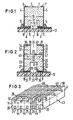
- the ceramic body 1 consists of varistor material and has two end faces 2 and 3.
- Metal coatings 4 and 5 are applied as electrodes on the surfaces adjacent to the end faces.
- the parts 6 and 7 of the metal coverings 4 and 5 extend to the end faces 2.
- the parts 8 and 9 of the metal coverings 4 and 5 extend to the end face 3 and serve there to rest on the conductor contact surfaces 10 and 11, which are attached to the insulating plate 12.
- solder 13 and 14 there is a risk that the parts 8 and 9 will be extended by excess solder residues 15 and 16.
- the previously defined distance 17 between the ends of the parts 8 and 9 is reduced to an undetermined distance 18.
- the thickness 19 of the ceramic body which should actually determine the distance between the coatings 4 and 5 and thus the mode of operation of the varistor, is considerably reduced as a result. Since the varistor voltage is a function of the distance between the metal assignments and since no current flows in the varistor at a voltage parallel to the varistor that is less than the varistor voltage, the distance 18 is decisive for this varistor.
- a current path is preferably formed only between parts 8 and 9 of metal coverings 4 and 5 (surface element), but not between metal coverings 4 and 5 itself.
- the varistor volume involved in the function which is decisive for the level of energy absorption, is reduced very strongly in this way, so that even considerably lower loads lead to a malfunction.
- the present invention has for its object to provide a varistor and a method for its production, which is suitable for higher varistor voltages and can be installed as a chip in printed circuits; the process should enable rational production.
- the varistor of the type mentioned is characterized according to the invention in that the ceramic body is provided at least on its side facing the GS plate with a depression which forms two side parts, that parts of the metal coverings reach the end faces of the side parts and that The width and depth of the depression are dimensioned such that the current path along the surface parts of the depression between the ends of the parts on the end faces of the side parts is longer than the distance between the metal coatings corresponding to the thickness of the ceramic body.
- the ceramic body preferably has only one depression, and in this case the metal coatings do not extend to the flat end face of the asymmetrical ceramic body that is then present.
- the ceramic body is only countersunk if parts of the metal coverings extend onto the then flat end face of the asymmetrical ceramic body and the current path between the ends of the parts on the end faces of the side parts is longer than the distance between the ends of the on the flat end surface protruding parts of the metal coverings.
- This embodiment makes it possible to vary the response voltage of the varistor, since the thickness of the ceramic body is fixed after the sintering so that the electrode spacing can be determined by the parts of the metal coverings that reach the flat end face.
- the method for producing a varistor of the invention in which bodies are formed and sintered from ceramic powdery varistor material, which are then provided with the metal coatings and are finished, as is known, according to the invention is characterized in that the object is characterized in that from the ceramic powdery varistor material first by Pressing or extruding a body on one or both sides with parallel bumps providing the later depressions is produced for a large number of varistors that the width of the elevations between the channels - taking into account the shrinkage during the later sintering firing - corresponds to twice the width of the side parts and that the body is then divided into parallel, mutually perpendicular separating surfaces before or after the sintering fire into the individual varistors.
- the advantages of the invention are that there is now a varistor that can be attached as a chip on printed circuit traces, the electrical properties of this varistor being determined by the thickness of the ceramic body, namely the distance between the metal coatings applied to the side surfaces can be determined.
- the symmetrical shape of the varistor ie with two depressions in the ceramic body, offers the advantage that such a varistor does not pose any problems for automatic assembly of the printed circuit board.
- the advantage of the asymmetrical shape, ie with only one depression in the ceramic body is that material can be saved.
- the manufacturing process is particularly simple, especially if the individual varistors are already produced from the body produced by extrusion or pressing for a large number of varistors before the sintering by appropriate division of the body and z.
- B. be sintered as bulk material or in particular on firing mats.
- a ceramic body 20 made of varistor material, namely the material used and known for this purpose with zinc oxide and various admixtures.
- the ceramic body 20 has, on opposite side surfaces, metal coatings 23 and 24, which serve as electrodes, are produced by known metallization processes (chemical, electrochemical, immersion in liquid metal, metal spraying processes, screen printing) and are made of nickel, nickel compounds, aluminum, Silver, etc. exist.
- the ceramic body 20 is provided with two depressions 25 and 26, the depression 25 facing the GS plate 12 and the depression 26 facing away from the GS plate 12.
- the depression 25 forms the side parts 27 and 28 with the end faces 29 and 30.
- the depression 26 forms the side parts 31 and 32 with the end faces 33 and 34.
- the part 35 of the metal coating 23 extends onto the end surface 29 and the part 36 of the metal covering 24 extends onto the end surface 30.
- the depth and the width of the depression 25 are dimensioned such that the current path 41 along the surfaces of the depression 25 is greater than the distance 42 of the metal coatings 23 and 24, which corresponds to the thickness of the ceramic body 20.
- parts 46 and 47 of the metal coatings 23 and 24 produced here in the same way as for the symmetrical shape can extend to the flat end face 22 of the asymmetrical ceramic body 20.
- the distance between the ends of the parts 46 and 47 is to be formed so that it is less than the current path 41 between the ends 39 and 40 of the metal coverings on the end faces 29 and 30 of the side parts 27 and 28 such a varistor is only effective in the surface area of the end face 22 between the ends of the parts 46 and 47 (surface element) and is therefore suitable for lower response voltages.
- FIG. 3 shows a body 43 produced by pressing or extrusion for a multiplicity of ceramic bodies 20.
- the body 43 has grooves 49 on one or both sides, which result in the later depressions 25 and 26.
- the width of the elevations 50 between the inland 49 is dimensioned taking into account the shrinkage during the ceramic sintering so that it corresponds to twice the width of the side parts 27, 28, 31, 32.
- the body 43 is preferably divided into the individual ceramic bodies 20 along parallel, mutually perpendicular separating surfaces 44 and 45 before the sintering firing, but possibly also after the sintering firing.
- a body is produced which is delimited by the area 51.
- the body 43 in terms of its dimensions such that two asymmetrical varistor bodies result from a symmetrical ceramic body 20 by appropriate division.
- the boundary surface 51 then runs in the middle between the grooves 49 located on the top and on the bottom.
- the finished varistors can be surrounded with insulating material, in particular plasma-sprayed aluminum oxide or high-temperature-resistant resins such as high-temperature epoxy resin or polyimide lacquer, provided that this does not affect the points to be soldered for the connection to the contact surfaces of the GS plates.
- the depressions 25 and possibly 26 can also be filled with this insulating material.
Landscapes
- Engineering & Computer Science (AREA)
- Microelectronics & Electronic Packaging (AREA)
- Physics & Mathematics (AREA)
- Electromagnetism (AREA)
- Thermistors And Varistors (AREA)
- Apparatuses And Processes For Manufacturing Resistors (AREA)
Abstract
Description
Die Erfindung betrifft einen Varistor in Chip-Bauweise zur Verwendung in gedruckten Schaltungen (GS) für auf Leiterbahnkontaktflächen einer GS-Platte aufliegenden Einbau, bestehend aus einem quaderförmigen Keramikkörper aus Varistormaterial, der an gegenüberliegenden Flächen mit lötfähigen Metallbelegungen als Elektrode versehen iet, die wenigstens auf die der GS-Platte zugewandte Fläche des Keramikkörpers reichen.The invention relates to a varistor in chip design for use in printed circuits (GS) for installation on conductor contact surfaces of a GS plate, consisting of a cuboid ceramic body made of varistor material, which is provided on opposite surfaces with solderable metal coatings as an electrode, at least on the area of the ceramic body facing the GS plate is sufficient.
Gedruckte Schaltungen sind in aller Regel so ausgeführt, daß in einem bestimmten Rastermaß - meist ein ganzzahliges Vielfaches von 2,5 mm - angeordnete Kontaktstellen (Löcher für Stromzuführungsdrähte elektrischer Bauelemente oder Kontakflächen für Bauelemente in Chip-Bauweise) durch Leiterbahnen entsprechend der gewünschten Schaltungsanordnung miteinander verbunden sind. Die elektrischen Bauelemente müssen für solche gedruckte Schaltungen derart ausgeführt sein, daß ihre Stromzuführungsflächen bei Bauelementen in Chip-Bauweise diesem Rastermaß entsprechen.Printed circuits are usually designed so that arranged contact points (holes for power supply wires of electrical components or contact surfaces for components in chip design) are connected to one another in a certain grid dimension - usually an integer multiple of 2.5 mm - by conductor tracks according to the desired circuit arrangement are. The electrical components for such printed circuits must be designed in such a way that their current supply surfaces for components in chip design correspond to this grid dimension.
In der DE-OS 2 528 090 ist ein Polyphasen-Stoßspannungsunterdrücker beschrieben, der aus einer Scheibe aus polykristallinem Varistormaterial mit einem Paar gegenüberliegender Flächen besteht, wobei eine Vielzahl von Kerben in dieser Scheibe angeordnet ist, die sich von einer ersten der genannten Flächen für einen Teil der Dicke in die Scheibe erstrecken, wobei ferner eine Vielzahl von Elektroden vorgesehen ist, die auf der ersten Fläche zwischen den Kerben angeordent sind, und wobei Mittel zum Verbinden der Vielzahl der Elektroden mit einem elektrischen Stromkreis vorhanden sind, sowie eine Elektrode, die auf einer zweiten der genannten Flächen angeordnet ist. Dieser Varistor ist für den Einbau in gedruckte Schaltungen im Prinzip nicht vorgesehen, denn er ist vollständig von Isoliermaterial umhüllt, aus dem die genannten Elektroden in Drathform herausragen. Gleichwohl ist in dieser Vorveröffentlichung beschreiben, daß jede der Kerben zwei Kanten aufweist, die der ersten der genannten Flächen benachbart sind, und mindestens eine Oberfläche zwischen diesen Kanten enthält, wobei der kürzeste Abstand zwischen den Kanten entlang der Oberfläche größer ist als die Dicke der Scheibe, die für die dortigen Zwecke gering zu wählen ist. Dieser kürzeste Abstand soll dort vorzugweise größer als das 2,3-fache der Dicke der Scheibe sein. Bei der Vierzahl der auf diese Scheibe aufzubringenden Elektroden und der dafür in die Scheibe einzubringenden Kerben leidet die mechanische Stabilität der Scheibe, denn wenn die Dicke der Scheibe größer gewählt wird, dann müssen die Kerben entsprechend tiefer sein und es verändern sich auch die von dem Varistor geforderten elektrischen Eigenschaften, weil dadurch der Abstand der Elektroden zur gemeinsamen Elektrode auf der gegenüberligenden Fläche der Scheibe größer wird.DE-OS 2 528 090 describes a polyphase surge suppressor which consists of a disk made of polycrystalline varistor material with a pair of opposing surfaces, a plurality of notches being arranged in this disk, which differ from a first of the said surfaces for one Extend part of the thickness into the disk, further comprising a plurality of electrodes arranged on the first surface between the notches, and means for connecting the plurality of electrodes to an electrical circuit, and an electrode which is on a second of said surfaces is arranged. In principle, this varistor is not intended for installation in printed circuits, because it is completely covered by insulating material, from which the electrodes mentioned protrude in wire form. However, this prior publication describes that each of the notches has two edges adjacent to the first of said faces and contains at least one surface between these edges, the shortest distance between the edges along the surface being greater than the thickness of the disk , which should be chosen low for the purposes there. This shortest distance should preferably be greater than 2.3 times the thickness of the disk. The mechanical stability of the disk suffers from the number of electrodes to be applied to this disk and the notches to be introduced into the disk, because if the thickness of the disk is chosen larger, the notches must be correspondingly deeper and the varistor also change required electrical properties because this increases the distance between the electrodes and the common electrode on the opposite surface of the disk.
In der DE-OS-3 140 802 ist ebenfalls ein Mehrelektrodenvaristor beschrieben, bei dem der Varistorkörper zwei gegenüberliegende Flächen aufweist, wobei auf der großer Fläche mehrere Elektroden befestigt sind und so mehrere durch die Gegenelektrode der anderen Fläche einpolig miteinander verbundene Varistoren bildet werden; dieser Varistorkörper weist an seiner Mehrelektrodenfläche zwischen benachbarten Elektroden höckerartige Erhebungen mit gegenüberliegenden Seitenflächen auf, wobei die Elektrodenenden an diesen Seitenflächen so hoch gezogen sind, daß durch die Varistorkörpererhebung zwischen zwei benachbarten Elektroden ein weiterer Varistor gebildet wird. Auch dieser Varistor ist für den Einbau in gedruckte Schaltungen als Chip weder vorgesehen noch geeignet.DE-OS-3 140 802 also describes a multi-electrode varistor in which the varistor body has two opposing surfaces, with a plurality of electrodes being fastened on the large surface and thus forming a plurality of varistors connected to one another by the counter electrode of the other surface; this varistor body has on its multi-electrode surface between adjacent electrodes bump-like elevations with opposite side surfaces, the electrode ends on these side surfaces being pulled up so that a further varistor is formed by the varistor body elevation between two adjacent electrodes. This varistor, too, is neither intended nor suitable for installation in printed circuits as a chip.
In der DE-AS-2 345109 sind für den Einbau in gedruckte Schaltungen geeignete Keramikkondensatoren beschrieben, die aus einem flachrohrförmigen Hohlkörper bestehen und deren äußere Belegungen derart ausgestaltet sind, daß sie auf kontaktflächen der Leiterbahnen gedruckter Schaltungen aufgelegt und durch Löten befestigt werden können.DE-AS-2 345109 describes ceramic capacitors which are suitable for installation in printed circuits and which consist of a flat tubular hollow body and whose outer coatings are designed such that they can be placed on contact surfaces of the printed circuit printed circuit boards and fastened by soldering.
In der DE-OS-2 528 090 ist ein Polyphasen-Keramikkondensatoren in Chip-Bauweise beschrieben, bei denen der dielektrische Körper aus einem von Metallschichten als Beläge durchsetzten monolithischen Keramikkörper besteht. Auch bei diesem Keramikkondensator sind die äußeren Stromzuführungselemente derart angebracht, daß sie mit Kontaktflächen von Leiterbahnen gedruckter Schaltungen verbunden werden können.DE-OS-2 528 090 describes a polyphase ceramic capacitor in chip design, in which the dielectric body consists of a monolithic ceramic body penetrated by metal layers as coatings. In this ceramic capacitor, too, the external power supply elements are attached in such a way that they can be connected to contact surfaces of printed circuit conductor tracks.
In der Zeitschrift "IBM Technical Disclosure Bulletin", Vol. 25, No 10, March 1983, S. 5366 und 5367 sind ebenfalls keramische Vielschichtkondensatoren beschrieben, bei denen ein keramischer monolithischer Block mit alternierend zu verschiedenen Seiten bzw. Anschlußetellen ragenden Metallschichten durchsetzt ist. Dabei sind sowohl flachliegende Vielschichtkondensatoren in Chip-Bauweise, als auch aufrechtstehende Vielschichtkondensatoren mit einer der GS-Platten zugewandten Einsenkung für den Einsatz in gedruckte Schaltungen gezeigt und beschrieben.In the journal "IBM Technical Disclosure Bulletin", Vol. 25,
In der DE-OS-3 231 277 ist ein regenerierfähiger elektrischer Schichtkondensator in Chip-Bauart beschrieben, bei dem das Dielektrikum aus durch Glimmpolymerisation von Kunststoff hergestellten-Schichten besteht, die abwechselnd zu verschiedenen Seiten endend mit Metallschichten durchsetzt sind. Der Kondensator befindet sich auf einem Trägerkörper, und die gegenpoligen Beläge sind an verschiedenen Seiten herausgeführt und über die Seitenteile des Trägerkörpers zu sogenannten Distanzstücken geführt. Auf diesen Distanzstücken enden die als Stromzuführungen für den Kondensator dienenden Metallschichten, so daß dieser Kondensator übereinander gestapelt werden kann. Für den Einbau eines solchen Stapelkondensators auf einer Leiterplatte weist der unterste Trägerkörper eine ebene Unterseite auf, die mit Einkerbungen versehen ist. Diese Einkerbungen dienen dem Zweck, den zur Befestigung des Stapelkondensators erforderlichen Kleber nicht seitlich unter dem Chip hervorquellen und die Kontaktstellen verschmutzen zu lassen.DE-OS-3 231 277 describes a regenerable electrical layer capacitor in chip design, in which the dielectric consists of layers produced by glow polymerisation of plastic, which are alternately interspersed with metal layers ending on different sides. The capacitor is located on a carrier body, and the oppositely polarized linings are led out on different sides and guided to so-called spacers via the side parts of the carrier body. On this Spacers end the metal layers serving as power supplies for the capacitor, so that this capacitor can be stacked on top of one another. For the installation of such a stacked capacitor on a printed circuit board, the lowermost carrier body has a flat underside, which is provided with notches. These notches serve the purpose of not allowing the adhesive required for fastening the stacked capacitor to swell out laterally under the chip and to make the contact points dirty.
Um einen Varistor, der gewöhnlich aus einem kompakten Block oder einer Scheibe besteht, für den Einsatz als Chip in gedruckte Schaltungen geeignet zu machen, könnte man daran denken, den Varistorkörper an gegenüberliegenden Flächen mit Metallschichten zu versehen und diese zumindest auf die der Schaltungsplatte zugewandte Seite des Varistorkörpers zu verlängern.In order to make a varistor, which usually consists of a compact block or a disk, suitable for use as a chip in printed circuits, one could think of providing the varistor body with metal layers on opposite surfaces and at least on the side facing the circuit board to extend the varistor body.
Ein solcher Varistor ist in Fig. 1 gezeigt und ist nicht Gegenstand der vorliegenden Erfindung. Der Keramikkörper 1 besteht aus Varistormaterial und weist zwei Stirnflächen 2 und 3 auf. Auf den den Stirnflächen benachbarten Flächen sind Metallbelegungen 4 und 5 als Elektroden aufgetragen. Der Teile 6 und 7 der Metallbelegungen 4 und 5 reichen bis auf die Stirnflächen 2.Such a varistor is shown in Fig. 1 and is not the subject of the present invention. The
Die Teile 8 und 9 der Metallbelegungen 4 und 5 reichen auf die Stirnfläche 3 und dienen dort zur Auflage auf den Leiterbahnkontaktflächen 10 und 11, die auf der Isolierstoffplatte 12 angebracht sind. Beim Befestigen des Varistors auf der gedruckten Schaltung mittels Lot 13 und 14 besteht die Gefahr, daß die Teile 8 und 9 durch überschüssige Lotreste 15 und 16 verlängert werden. Dadurch wird der vorherige festgelegte Abstand 17 zwischen den Enden der Teile 8 und 9 auf einen unbestimmten Abstand 18 verringert. Die Dicke 19 des Keramikkörpers, die eigentlich den Abstand zwischen den Belegungen 4 und 5 und damit die Wirkungsweise des Varistors bestimmen sollte, wird dadurch noch erheblich weiter verringert. Da die Varistorspannung eine Funktion dee Abstandes zwischen den Metallbelegungen ist und da bei einer Spannung parallel zum Varistor, die geringer ist ale die Varistorspannung, kein Strom in dem Varistor fließt, ist für diesen Varistor der Abstand 18 maßgebend.The
Zusätzlich bildet sich ein Strompfad bevorzugt nur zwischen den Teilen 8 und 9 der Metallbelegungen 4 und 5 (Oberflächenelement), nicht jedoch zwischen den Metallbelegungen 4 und 5 selbst aus. Das in die Funktion einbezogene Varistorvolumen, das für die Höhe der Energieabsorption maßgeblich ist, ist auf diese Weise sehr starkt reduziert, so daß bereits wesentlich geringere Belastungen zu einem Funktionsausfall führen.In addition, a current path is preferably formed only between
Der vorliegenden Erfindung liegt die Aufgabe zugrunde, einen Varistor und ein Verfahren zu seiner Herstellung anzugeben, der für höhere Varistorspannungen geeignet und als Chip in gedruckte Schaltungen einbaubar ist; das Verfahren soll eine rationelle Herstellung ermöglichen.The present invention has for its object to provide a varistor and a method for its production, which is suitable for higher varistor voltages and can be installed as a chip in printed circuits; the process should enable rational production.
Zur Lösung dieser Aufgabe ist der Varistor der eingangs angegebenen Art erfindungsgemäß dadurch gekennzeichnet, daß der Keramikkörper wenigstens auf seiner der GS-Platte zugewandten Seite mit einer Einsenkung versehen ist, die zwei Seitenteile bildet, daß Teile der Metallbelegungen auf die Stirnflächen der Seitenteile reichen und daß Breite und Tiefe der Einsenkung so bemessen sind, daß der Stromweg längs der Oberflächenteile der Einsenkung zwischen den Enden der Teile auf den Stirnflächen der Seitenteile länger ist als der der Dicke des Keramikkörpers entsprechende Abstand zwischen den Metallbelegungen.To solve this problem, the varistor of the type mentioned is characterized according to the invention in that the ceramic body is provided at least on its side facing the GS plate with a depression which forms two side parts, that parts of the metal coverings reach the end faces of the side parts and that The width and depth of the depression are dimensioned such that the current path along the surface parts of the depression between the ends of the parts on the end faces of the side parts is longer than the distance between the metal coatings corresponding to the thickness of the ceramic body.
Vorzugsweise weist der Keramikkörper nur eine Einsenkung auf, und die Metallbelegungen reichen in diesem Falle nicht bis auf die dann vorhandene ebene Stirnfläche des asymmetrischen Keramikkörpers.The ceramic body preferably has only one depression, and in this case the metal coatings do not extend to the flat end face of the asymmetrical ceramic body that is then present.
Andererseits ist es bei nur einer Einsenkung des Keramikkörpers vorteilhaft, wenn Teile der Metallbelegungen auf die dann vorhandene ebene Stirnfläche des asymmetrischen Keramikkörpers reichen und der Stromweg zwischen den Enden der Teile auf den Stirnflächen der Seitenteile länger ist, als der Abstand zwischen den Enden der auf die ebene Stirnfläche ragenden Teile der Metallbelegungen.On the other hand, it is advantageous if the ceramic body is only countersunk if parts of the metal coverings extend onto the then flat end face of the asymmetrical ceramic body and the current path between the ends of the parts on the end faces of the side parts is longer than the distance between the ends of the on the flat end surface protruding parts of the metal coverings.
Diese Ausführungsform ermöglicht es, die Ansprechspannung des Varistors zu variieren, da die Dicke des Keramikkörpers nach dem Sinterbrand festliegt, so daß durch die auf die ebene Stirnfläche reichende Teile der Metallbelegungen der Elektrodenabstand festgelegt werden kann.This embodiment makes it possible to vary the response voltage of the varistor, since the thickness of the ceramic body is fixed after the sintering so that the electrode spacing can be determined by the parts of the metal coverings that reach the flat end face.
Das Verfahren zur Herstellung eines Varistors der Erfindung, bei dem aus keramischem pulverförmigem Varistormaterial Körper geformt und gesintert werden, die dann mit den Metallbelegungen versehen und wie bekannt fertiggestellt werden, ist zur Lösung der Aufgabe erfindungegemäß dadurch gekennzeichnet, daß aus dem keramischen pulverförmigen Varistormaterial zunächst durch Pressen oder Strangziehen ein ein- oder beidseitig mit parallel verlaufenden, die späteren Einsenkungen ergebenden Billen versehender Körper für eine Vielzahl von Varistoren erzeugt wird, daß die Breite der Erhebungen zwischen den Rinnen - die Schwindung beim späteren Sinterbrand berücksichtigend - der doppelten Breite der Seitenteile entspricht und daß dann der Körper längs paralleler, zueinander senkrecht stehender Trennflächen vor oder nach dem Sinterbrand in die einzelnen Varistoren aufgeteilt wird.The method for producing a varistor of the invention, in which bodies are formed and sintered from ceramic powdery varistor material, which are then provided with the metal coatings and are finished, as is known, according to the invention is characterized in that the object is characterized in that from the ceramic powdery varistor material first by Pressing or extruding a body on one or both sides with parallel bumps providing the later depressions is produced for a large number of varistors that the width of the elevations between the channels - taking into account the shrinkage during the later sintering firing - corresponds to twice the width of the side parts and that the body is then divided into parallel, mutually perpendicular separating surfaces before or after the sintering fire into the individual varistors.
Die Vorteile der Erfindung bestehen darin, daß nun ein Varistor vorliegt, der als Chip auf Leiterbahnen gedruckter Schaltungen befestigt werden kann, wobei die elektrischen Eigenschaften dieses Varistors durch die Dicke des Keramikkörpers, nämlich den Abstand zwischen den auf den Seitenflächen aufgebrachten Metallbelegungen bestimmt werden. Die symmetrische Form des Varistors, d.h. mit zwei Einsenkungen im Keramikkörper, bietet den Vorteil, daß ein solcher Varistor für eine automatische Bestückung der Leiterplatte keine Probleme bringt. Der Vorteil der asymmetrischen Form, d.h. mit nur einer Einsenkung im Keramikkörper, besteht darin, daß Material eingespart werden kann.The advantages of the invention are that there is now a varistor that can be attached as a chip on printed circuit traces, the electrical properties of this varistor being determined by the thickness of the ceramic body, namely the distance between the metal coatings applied to the side surfaces can be determined. The symmetrical shape of the varistor, ie with two depressions in the ceramic body, offers the advantage that such a varistor does not pose any problems for automatic assembly of the printed circuit board. The advantage of the asymmetrical shape, ie with only one depression in the ceramic body, is that material can be saved.
Das Herstellungsverfahren gestaltet sich besonders einfach, insbesondere dann, wenn aus dem durch Strangziehen oder Pressen hergestellten Körper für eine Viehlzahl von Varistoren die einzelnen Varistoren bereits vor dem Sintern durch ensprechende Aufteilung des Körpers erzeugt und z. B. als Schüttgut oder insbesondere auf Brennunterlagen gesintert werden.The manufacturing process is particularly simple, especially if the individual varistors are already produced from the body produced by extrusion or pressing for a large number of varistors before the sintering by appropriate division of the body and z. B. be sintered as bulk material or in particular on firing mats.
Die Erfindung wird nachfolgend anhand der Figuren näher erläutert.The invention is explained in more detail below with reference to the figures.
Es zeigen:
- Fig. 1 einen Varistor in Quaderform, der jedoch für den Einbau in gedruckten Schaltungen wenig geeignet ist;
- Fig. 2 einen Varistor nach der Erfindung und
- Fig. 3 einen Körper für viele einzelne Varistoren, der nach dem Verfahren der Erfindung hergestellt ist.
- Figure 1 shows a varistor in cuboid shape, but is not very suitable for installation in printed circuits.
- Fig. 2 shows a varistor according to the invention and
- Fig. 3 shows a body for many individual varistors, which is made by the method of the invention.
Der Varistor nach Fig. 1 ist bereits oben ausführlich beschrieben.1 has already been described in detail above.
Der Varistor nach Fig. 2 besteht aus einem Keramikkörper 20 aus Varistormaterial, nämlich das für diese Zwecke benutzte und bekannte Material mit Zinkoxid und verschiedenen Beimengungen.2 consists of a
Mit 21 ist eine Begrenzungslinie eingezeichnet, bis zu der der Keramikkörper gegebenenfalls reichen kann, wenn es sich um einen asymmetrischen Keramikkörper handeln soll. Ein solcher Körper weist dann die Stirnfläche 22 auf. Im übrigen wird dieser asymmetrische Varistor später noch näher erläutert.With 21 a boundary line is drawn, up to which the ceramic body can possibly extend if it is to be an asymmetrical ceramic body. Such a body then has the
Bei der symmetrischen Ausführungsform des Varistors besitzt der Keramikkörper 20 an gegenüberliegenden Seitenflächen Metallbelegungen 23 und 24, die als Elektroden dienen, durch bekannte Metallisierverfahren (chemisch, elektrochemisch, Tauchen in flüssiges Metall, Metallspritzverfahren, Siebdrucken) hergestellt sind und aus Nickel, Nickelverbindungen, Aluminium, Silber usw. bestehen.In the symmetrical embodiment of the varistor, the
Der Keramikkörper 20 ist mit zwei Einsenkungen 25 und 26 versehen, wobei die Einsenkung 25 der GS-Platte 12 zugewandt ist und die Einsenkung 26 von der GS-Platte 12 abgewandt ist.The
Die Einsenkung 25 bildet die Seitenteile 27 und 28 mit den Stirnflächen 29 und 30.The
Die Einsenkung 26 bildet die Seitenteile 31 und 32 mit den Stirnflächen 33 und 34. Der Teil 35 der Metallbelegung 23 reicht auf die Stirnfläche 29, und der Teil 36 der Metallbelegung 24 reicht auf die Stirnfläche 30.The
Entsprechendes gilt für die andere Seite des Keramikkörpers 20; dort reicht der Teil 37 der Metallbelegung 24 auf die Stirnfläche 33, und der Teil 38 der Metallbelegung 23 reicht auf die Stirnfläche 34.The same applies to the other side of the
Mit 39 und 40 sind die Enden der Teile 35 bzw. 38 und 36 bzw. 37 bezeichnet. Diese Enden der Metallbelegungen reichen bis zu den Einsenkungen 25 und 26. Durch diese Ausgestaltung wird erreicht, daß Lotreste an den Leiterbahnkontaktflächen die elektrischen Eigenschaften des Varistors nicht mehr beeinflussen.With 39 and 40, the ends of the
Die Tiefe und die Breite der Einsenkung 25 (gleiches gilt für die Einsenkung 26) sind so bemessen, daß der Stromweg 41 längs den Oberflächen der Einsenkung 25 größer ist als der Abstand 42 der Metallbelegungen 23 und 24, der der Dicke des Keramikkörpers 20 entspricht.The depth and the width of the depression 25 (the same applies to the depression 26) are dimensioned such that the current path 41 along the surfaces of the
Bei einem asymmetrischen Varistor können Teile 46 und 47 der hier in gleicher Weise wie bei der symmetrischen Form hergestellten Metallbelegungen 23 und 24 bis auf die ebene Stirnfläche 22 des asymmetrischen Keramikkörpers 20 reichen. In diesem Fall ist jedoch der Abstand zwischen den Enden der Teile 46 und 47 so zu bilden, daß er geringer ist, als der Stromweg 41 zwischen den Enden 39 und 40 der Metallbelegungen auf den Stirnflächen 29 und 30 der Seitenteile 27 und 28. Allerdings ist ein solcher Varistor nur im Oberflächenbereich der Stirnfläche 22 zwischen den Enden der Teile 46 und 47 wirksam (Oberflächenelement) und deshalb für geringere Ansprechspannungen geeignet.In the case of an asymmetrical varistor,
In Fig. 3 ist ein durch Pressen oder Strangziehen erzeugter Körper 43 für eine Vielzahl von keramischen Körpern 20 gezeigt. Der Körper 43 weist auf einer oder auf beiden Seiten Rinnen 49 auf, die die späteren Einsenkungen 25 und 26 ergeben. Die Breite der Erhebungen 50 zwischen den Binnen 49 ist unter Berücksichtigung der Brennschwindung beim keramischen Sinterbrand so bemessen, daß sie der doppelten Breite der Seitenteile 27, 28, 31, 32 entspricht.FIG. 3 shows a
Vorzugsweise vor dem Sinterbrand, gegebenenfalls aber auch nach dem Sinterbrand wird der Körper 43 längs paralleler, aufeinander senkrecht stehender Trennflächen 44 und 45 in die einzelnen Keramikkörper 20 aufgeteilt.The
Bei der Herstellung asymmetrischer Varistoren wird ein Körper hergestellt, der durch die Fläche 51 begrenzt ist. Es ist aber auch möglich, den Körper 43 hinsichtlich seiner Abmessungen so zu gestalten, daß aus einem symmetrischen Keramikkörper 20 durch entsprechende Aufteilung zwei asymmetrische Varistorkörper resultieren. Die Begrenzungsfläche 51 verläuft dann in der Mitte zwischen den auf der Ober- und auf der Unterseite befindlichen Rinnen 49.When asymmetric varistors are produced, a body is produced which is delimited by the
Nach dem Sinterbrand der Keramikkörper 20 werden diese auf den dafür vorgesehenen Flächen mit Metallbelegungen versehen, wofür an sich bekannte Verfahren zur Metallisierung von Keramikkörpern geeignet sind. Gegebenenfalls können die fertigen Varistoren mit Isoliermaterial insbesondere plasmagespritztes Aluminiumoxid oder hochtemperaturbeständige Harze wie Hochtemperaturepoxidharz oder Polyimidlack, umgeben werden, sofern dadurch die zu lötenden Stellen für die Verbindung mit den Kontaktflächen der GS-Platten nicht beeinträchtigt werden. Somit können die Einsenkungen 25 und gegebenenfalls 26 mit diesem Isoliermaterial auch ausgefüllt sein.After the sintering of the
- 1 Keramikkörper aus Varistormaterial1 ceramic body made of varistor material
-
2 Stirnfläche des Keramikkörpers 12 end face of the
ceramic body 1 -
3 Stirnfläche des Keramikkörpers 1, der GS-Platte 12 zugewandt3 face of the
ceramic body 1, theGS plate 12 facing - 4 Metallbelegung als Elektrode4 metal coating as electrode
- 5 Metallbelegung als Elektrode5 metal coating as electrode
- 6 Teil der Metallbelegung 4, der gegebenenfalls auf die Stirnfläche 2 reicht,6 part of the metal covering 4, which possibly extends to the end face 2,
- 7 Teil der Metallbelegung 5, der gegebenenfalls auf die Stirnfläche 2 reicht,7 part of the metal covering 5, which possibly extends to the end face 2,
-
8 Teil der Metallbelegung 4, der auf die Stirnfläche 3 reicht8 part of the metal covering 4, which extends to the
end face 3 -
9 Teil der Metallbelegung 5, der auf die Stirnfläche 3 reicht9 part of the metal coating 5, which extends to the
end face 3 - 10 Leiterbahnkontaktfläche10 conductor contact area
- 11 Leiterbahnkontaktfläche11 conductor contact area
- 12 Leiterbahnplatte aus Isolierstoff (GS-Platte)12 conductor plate made of insulating material (GS plate)
-
13 Lot, das die Leiterbahnkontaktfläche 10 mit dem Teil 8 und der Teilbelegung 4 verbindet13 solder that connects the conductor
track contact surface 10 with thepart 8 and thepart assignment 4 -
14 Lot, das die Leiterbahnkontaktfläche 11 mit dem Teil 9 und der Metallbelegung 5 verbindet14 solder that connects the conductor
track contact surface 11 with the part 9 and the metal coating 5 - 15 Lotrest15 solder residue
- 16 Lotrest16 solder residue
- 17 gewünschter Elektrodenabstand17 desired electrode spacing
- 18 verringerter Elektrodenabstand18 reduced electrode spacing
- 19 Dicke des Keramikkörpers19 thickness of the ceramic body
- 20 Keramikkörper aus Varistormaterial20 ceramic bodies made of varistor material
-
21 Begrenzungslinie, bis zu der ein asymmetrischer Keramikkörper 20 gegebenenfalls reicht21 boundary line up to which an asymmetrical
ceramic body 20 may extend -
22' ebene Stirnfläche eines asymmetrischen Keramikkörpers 2022 'flat end face of an asymmetrical
ceramic body 20 - 23 Metallbelegung als Elektrode23 Metal coating as an electrode
- 24 Metallbelegung als Elektrode24 metal coating as electrode
-
25 Einsenkung im Keramikkörper 20, der GS-Platte 12 zugewandt25 depression in the
ceramic body 20, facing theGS plate 12 -
26 Einsenkung im Keramikkörper 20, von der GS-Platte 12 abgewandt26 countersink in the
ceramic body 20, facing away from theGS plate 12 -
27 Seitenteil der Einsenkung 2527 side part of the
depression 25 -
28 Seitenteil der Einsenkung 2528 side part of the
depression 25 -
29 Stirnfläche des Seitenteiles 2729 end face of the
side part 27 -
30 Stirnfläche des Seitenteiles 2830 end face of the
side part 28 -
31 Seitenteil der Einsenkung 2631 side part of the
depression 26 -
32 Seitenteil der Einsenkung 2632 side part of the
depression 26 - 33 Stirnfläche des Seitenteiles 3133 end face of the side part 31
-
34 Stirnfläche des Seitenteiles 3234 end face of the
side part 32 -
35 Teil der Metallbelegung 23, der auf die Stirnfläche 29 reicht35 part of the
metal coating 23, which extends to theend face 29 -
36 Teil der Metallbelegung 24, der auf die Stirnfläche 30 reicht36 part of the
metal coating 24, which extends to theend face 30 -
37 Teil der Metallbelegung 24, der auf die Stirnfläche 33 reicht37 part of the
metal coating 24, which extends to the end face 33 -
38 Teil der Metallbelegung 23, der auf die Stirnfläche 34 reicht38 part of the
metal coating 23, which extends to theend face 34 -
39 Enden der Teile 35 und 3839 ends of
parts 35 and 38 -
40 Enden der Teile 36 und 3740 ends of
parts 36 and 37 -
41 Stromweg an den Oberflächen der Einsenkung 2541 current path on the surfaces of the
depression 25 -
42 Abstand der Metallbelegungen 23 und 24, entsprechend der Dicke des Keramikkörpers 2042 distance of the
metal coatings - 43 durch Pressen hergestellter Körper vor oder nach der Sinterung43 bodies produced by pressing before or after sintering
- 44 Parallele Trennflächen44 Parallel parting surfaces
- 45 Parallele Trennflächen, senkrecht zu den Trennflächen 4445 Parallel dividing surfaces, perpendicular to the dividing surfaces 44
-
46 Teil der Metallbelegung 23, der auf die Stirnfläche 22 reicht46 part of the
metal coating 23, which extends to theend face 22 -
47 Teil der Metallbelegung 24, der auf die Stirnfläche 22 reicht47 part of the
metal coating 24, which extends to theend face 22 -
48 Abstand zwischen den Enden der Teile 46 und 4748 distance between the ends of
parts 46 and 47 -
49 Rinnen auf einer oder auf beiden Seiten des Körpers 4349 channels on one or both sides of the
body 43 - 50 Erhebungen zwischen den Rinnen 4950 elevations between the channels 49
-
51 Begrenzung des Körpers 43 für die Herstellung von Varistoren mit nur einer Einsenkung 2551 Limitation of the
body 43 for the production of varistors with only onedepression 25
Claims (4)
Priority Applications (1)
| Application Number | Priority Date | Filing Date | Title |
|---|---|---|---|
| AT85109001T ATE34482T1 (en) | 1984-07-31 | 1985-07-18 | VARISTOR IN CHIP CONSTRUCTION FOR USE IN PRINTED CIRCUITS AND METHOD FOR ITS MANUFACTURE. |
Applications Claiming Priority (2)
| Application Number | Priority Date | Filing Date | Title |
|---|---|---|---|
| DE3428242 | 1984-07-31 | ||
| DE3428242 | 1984-07-31 |
Publications (2)
| Publication Number | Publication Date |
|---|---|
| EP0171642A1 EP0171642A1 (en) | 1986-02-19 |
| EP0171642B1 true EP0171642B1 (en) | 1988-05-18 |
Family
ID=6242037
Family Applications (1)
| Application Number | Title | Priority Date | Filing Date |
|---|---|---|---|
| EP85109001A Expired EP0171642B1 (en) | 1984-07-31 | 1985-07-18 | Chip varistor for use in printed circits, and method of producing it |
Country Status (3)
| Country | Link |
|---|---|
| EP (1) | EP0171642B1 (en) |
| AT (1) | ATE34482T1 (en) |
| DE (1) | DE3562835D1 (en) |
Families Citing this family (3)
| Publication number | Priority date | Publication date | Assignee | Title |
|---|---|---|---|---|
| DE3445698A1 (en) * | 1984-12-14 | 1986-06-26 | C. Conradty Nürnberg GmbH & Co KG, 8505 Röthenbach | CHIP VARISTOR AND METHOD FOR THE PRODUCTION THEREOF |
| NL8800156A (en) * | 1988-01-25 | 1989-08-16 | Philips Nv | CHIP RESISTOR AND METHOD FOR MANUFACTURING A CHIP RESISTOR. |
| US5287083A (en) * | 1992-03-30 | 1994-02-15 | Dale Electronics, Inc. | Bulk metal chip resistor |
Family Cites Families (5)
| Publication number | Priority date | Publication date | Assignee | Title |
|---|---|---|---|---|
| US4364021A (en) * | 1977-10-07 | 1982-12-14 | General Electric Company | Low voltage varistor configuration |
| US4157527A (en) * | 1977-10-20 | 1979-06-05 | General Electric Company | Polycrystalline varistors with reduced overshoot |
| DE3277042D1 (en) * | 1981-02-13 | 1987-09-24 | Gen Electric | Zinc oxide varistor with reduced fringe current effects |
| FR2513032B1 (en) * | 1981-09-14 | 1985-12-13 | Carreras Michelle | INTEGRATED PROTECTION AGAINST OVERVOLTAGES OF AN ELECTRONIC CIRCUIT, AND ELECTRONIC CIRCUIT PROTECTED BY THIS DEVICE |
| US4451815A (en) * | 1982-09-27 | 1984-05-29 | General Electric Company | Zinc oxide varistor having reduced edge current density |
-
1985
- 1985-07-18 EP EP85109001A patent/EP0171642B1/en not_active Expired
- 1985-07-18 AT AT85109001T patent/ATE34482T1/en active
- 1985-07-18 DE DE8585109001T patent/DE3562835D1/en not_active Expired
Also Published As
| Publication number | Publication date |
|---|---|
| EP0171642A1 (en) | 1986-02-19 |
| DE3562835D1 (en) | 1988-06-23 |
| ATE34482T1 (en) | 1988-06-15 |
Similar Documents
| Publication | Publication Date | Title |
|---|---|---|
| DE3738343C2 (en) | ||
| EP2201585B1 (en) | Electric multilayer component | |
| DE3612084C2 (en) | ||
| DE2940339C2 (en) | ||
| DE4244064C2 (en) | Device for a vehicle | |
| DE3927711C2 (en) | Laminated inductance | |
| DE3416107A1 (en) | BUS LINE ARRANGEMENT WITH HIGH CAPACITY IN LAYER DESIGN | |
| EP0171642B1 (en) | Chip varistor for use in printed circits, and method of producing it | |
| DE2929547C2 (en) | Microwave attenuator | |
| DE19627543A1 (en) | Multilayer substrate for printed circuit board | |
| DE2526553C3 (en) | Multilayer electronic circuit and method for its manufacture | |
| WO1985000085A1 (en) | Printed board for the surface soldering of integrated miniature circuits and manufacturing method of such printed boards | |
| DE3211540A1 (en) | MINIATURE HIGH CAPACITY RAIL AND METHOD FOR PRODUCING THE SAME | |
| DE3222938A1 (en) | Multilayer ceramic plate | |
| DE2020535C3 (en) | Process for producing electrical conductors in printed circuits and electrical conductors produced by this process | |
| DE10057606B4 (en) | Arrangement for connecting the ferrite core of a planar transformer to ground | |
| DE4422669A1 (en) | Multilayer circuit board design | |
| DE3438062C1 (en) | Interference protection capacitor arrangement and method for its production | |
| DE3240412A1 (en) | LAMINATED HIGH CAPACITY BUSBAR | |
| DE1614591C (en) | Stacked capacitor that can be adjusted to a desired nominal value of its capacitance | |
| DE2055236A1 (en) | A spool printed on a double-laminated board | |
| EP0472817A2 (en) | Electrostatic spray pistol | |
| DE2623640A1 (en) | ELECTRICAL FILM RESISTOR AND METHOD OF ITS MANUFACTURING | |
| DE1764214C (en) | capacitor | |
| DE4410753A1 (en) | Capacitor array |
Legal Events
| Date | Code | Title | Description |
|---|---|---|---|
| PUAI | Public reference made under article 153(3) epc to a published international application that has entered the european phase |
Free format text: ORIGINAL CODE: 0009012 |
|
| AK | Designated contracting states |
Designated state(s): AT DE FR GB IT |
|
| 17P | Request for examination filed |
Effective date: 19860307 |
|
| 17Q | First examination report despatched |
Effective date: 19870804 |
|
| GRAA | (expected) grant |
Free format text: ORIGINAL CODE: 0009210 |
|
| AK | Designated contracting states |
Kind code of ref document: B1 Designated state(s): AT DE FR GB IT |
|
| REF | Corresponds to: |
Ref document number: 34482 Country of ref document: AT Date of ref document: 19880615 Kind code of ref document: T |
|
| REF | Corresponds to: |
Ref document number: 3562835 Country of ref document: DE Date of ref document: 19880623 |
|
| GBT | Gb: translation of ep patent filed (gb section 77(6)(a)/1977) | ||
| ET | Fr: translation filed | ||
| ITF | It: translation for a ep patent filed | ||
| PLBE | No opposition filed within time limit |
Free format text: ORIGINAL CODE: 0009261 |
|
| STAA | Information on the status of an ep patent application or granted ep patent |
Free format text: STATUS: NO OPPOSITION FILED WITHIN TIME LIMIT |
|
| PG25 | Lapsed in a contracting state [announced via postgrant information from national office to epo] |
Ref country code: FR Free format text: LAPSE BECAUSE OF NON-PAYMENT OF DUE FEES Effective date: 19890331 |
|
| PG25 | Lapsed in a contracting state [announced via postgrant information from national office to epo] |
Ref country code: DE Effective date: 19890401 |
|
| 26N | No opposition filed | ||
| REG | Reference to a national code |
Ref country code: FR Ref legal event code: ST |
|
| PG25 | Lapsed in a contracting state [announced via postgrant information from national office to epo] |
Ref country code: GB Effective date: 19890718 Ref country code: AT Effective date: 19890718 |
|
| GBPC | Gb: european patent ceased through non-payment of renewal fee |