EP0171509B1 - Silicon on sapphire laser process - Google Patents
Silicon on sapphire laser process Download PDFInfo
- Publication number
- EP0171509B1 EP0171509B1 EP85104750A EP85104750A EP0171509B1 EP 0171509 B1 EP0171509 B1 EP 0171509B1 EP 85104750 A EP85104750 A EP 85104750A EP 85104750 A EP85104750 A EP 85104750A EP 0171509 B1 EP0171509 B1 EP 0171509B1
- Authority
- EP
- European Patent Office
- Prior art keywords
- silicon
- island
- silicon island
- radiation beam
- conductor
- Prior art date
- Legal status (The legal status is an assumption and is not a legal conclusion. Google has not performed a legal analysis and makes no representation as to the accuracy of the status listed.)
- Expired - Lifetime
Links
Images
Classifications
-
- H—ELECTRICITY
- H10—SEMICONDUCTOR DEVICES; ELECTRIC SOLID-STATE DEVICES NOT OTHERWISE PROVIDED FOR
- H10P—GENERIC PROCESSES OR APPARATUS FOR THE MANUFACTURE OR TREATMENT OF DEVICES COVERED BY CLASS H10
- H10P34/00—Irradiation with electromagnetic or particle radiation of wafers, substrates or parts of devices
- H10P34/40—Irradiation with electromagnetic or particle radiation of wafers, substrates or parts of devices with high-energy radiation
- H10P34/42—Irradiation with electromagnetic or particle radiation of wafers, substrates or parts of devices with high-energy radiation with electromagnetic radiation, e.g. laser annealing
Definitions
- This invention is related to metal oxide semiconductor devices formed in silicon on sapphire in which the channel mobility is increased.
- MOS metal oxide semiconductor
- FET field effect transistor
- SOS silicon on sapphire
- a significant problem in the art of silicon on sapphire (SOS) is the low channel mobility which results from a high defect density at the top epitaxial silicon surface. Reduction in channel mobility decreases the device operating speed.
- aluminium conductors interconnecting between individual MOSFETS on the sapphire substrate must cover a nearly vertical step formed at the edge of each silicon island.
- a reduction in the thickness of the deposited aluminium conductor and cracks in the aluminium may occur in the vicinity of a vertical step.
- Such cracks and reduction in the thickness of the deposited aluminium increases the likelihood of discontinuities in the aluminium conductor which cause device failure.
- Another problem which is peculiar to SOS devices is that growth of a silicon dioxide layer over the silicon island usually is accompanied by a region of reduced oxide thickness resulting in a "V"-shaped groove at the lower corner of each silicon island edge. If a polycrystalline silicon conductive layer is deposited or grown thereover, the amount of insulation between the overlying polysilicon conductor and the silicon island is greatly reduced at the V-shaped groove, thereby increasing the likelihood of breakdown conduction through the insulating oxide film between the polysilicon conductor and the silicon island.
- a beam of radiant energy such as a laser beam is applied to the silicon island before formation of the overlying insulating and conducting layers.
- the energy and power density of the beam are sufficient to melt of the top epitaxial silicon layer, with a con- commitant enhancement of channel mobility.
- Carrier mobility in thin surface regions of a given area of semicondutor material is improved by rapidly heating the surface area to or slightly above the melting point of the semiconductor material and then allowing the material to rapidly cool below its melting point in the recrystallisation process. Significantly, this in turn leads to an increase in the speed of transistors formed in the silicon.
- the exposure to a laser beam also causes the material in the silicon island edge to reflow, resulting in a reduction in the slope of the silicon island edge.
- the face of the silicon island edge becomes smoother during this reflow process, so that the roughness of the face is eliminated to provide a smooth and gradually sloping step.
- oxide film overlying the silicon island has a uniform thickness even in the vicinity of the bottom edge corner of the silicon island.
- the uniform thickness of the oxide film provides uniform insulation between an overlying polysilicon conductor and the silicon island, thereby eliminating the problem of breakdown conduction at the bottom edge corner of the silicon island.
- the present invention provides a method for increasing channel carrier mobility in a surface region of a silicon island formed on a sapphire substrate comprising irradiating a predetermined surface area of the silicon island with a pulsed radiation beam of a chosen wavelength, pulse duration and energy per unit area sufficient to elevate the temperature of only a thin surface layer bounded by said surface area to the melting point of the silicon, and thereafter allowing the silicon to cool below its melting point while recrystallizing to solid state.
- the silicon islands are exposed to radiation from an excimer laser emitting radiation having a wavelength of 2490 A, a pulse duration of 25 nanoseconds, a beam size in the range of 0.1 to 0.2 cm 2 and an energy density in the range of 0.5 to 1.0 joules/cm 2 .
- a pulsed ion beam or electron beam source may be used in a similar fashion.
- a first oxide layer is grown, followed by deposition and definition of polysilicon conductors, which are then implanted simultaneously with implantation of source and drain regions. Thereafter, a top oxide layer is deposited, contact openings are etched through the oxide layers followed by deposition and definition of aluminum conductors.
- the resulting step coverage of overlying aluminum conductors was found to be improved, the thickness of the aluminum conductors being uniform throughout the device, thereby solving the problem of discontinuities normally encountered in step coverage by the aluminum layer.
- FIG. 1 is a simplified cross sectional view of a silicon on sapphire (SOS) island including a sapphire substrate 1 and a silicon island 2 photolithographically defined by an etching process to form an island edge 3.
- the island edge 3 has a steep slope created during definition of the silicon island 2.
- a first oxide layer 6 is preferably grown over the top surface of the silicon island 2 and the thickness of the oxide layer 6 is reduced at a bottom edge corner 8 of the island, forming a "V" shaped groove 9.
- a polysilicon conductor 10 shown in FIG.'s 2 and 3 is formed by deposition of polycrystalline silicon followed by photolithographic definition and etching. The deposited polysilicon fills the V-shaped groove 9 so that there is a significant likelihood of breakdown conduction between the polysilicon conductor 10 and the silicon island 2 in the vicinity of the V-shaped groove 9.
- the polysilicon conductor 10 is deposited, photolithographically defined and etched. Thereafter, the device is ion implanted to render the polysilicon material conductive while simultaneously forming gatealigned source and drain diffusions in the silicon island 2, in a manner well known in the art. A second layer of oxide 11 is then placed over the device. Contacts (not shown) are defined through the oxide layers.
- An aluminium conductor 12 shown in Figures 2 and 4 is formed by evaporation followed by photolithographic definition and etching. Because the etching process which initially defines the edge 3 of the SOS island 2 shown in Figure 1 is not uniform, the resulting island edge 3 is rough.
- Figure 4 clearly shows that the thickness t 1 of the aluminium conductor 12 deposited over the steep island edge 3 is significantly reduced with respect to the aluminium thickness t 2 overlying horizontal surfaces. This reduction of the thickness of the aluminium conductor 12 at the edge 3 increases the probability of discontinuities in the conductor 12. As a result, it has been found that the processing yield of metal-oxide-semi-conductor silicon-on-sapphire (MOS/SOS) devices is significantly reduced.
- MOS/SOS metal-oxide-semi-conductor silicon-on-sapphire
- a pulsed beam 13 or radiant energy is directed from an energy source 14 such as a laser toward the silicon island 2 prior to the growth or deposition of overlying insulating and conductive layers.
- the drawing of Figure 5 is purely schematic and does not imply any restriction on required beam size.
- the energy beam improves the quality of the crystal structure of the silicon island 2, which increases the channel mobility of metal oxide semiconductor field effect transistors (MOSFET's) fabricated on the silicon island 2. It should be noted that, in order to increase mobility, the energy beam may be applied either before or after definition of the silicon island 2.
- MOSFET's metal oxide semiconductor field effect transistors
- MOS transistors Mobility in MOS transistors is a well known concept in the art and is discussed, for example, in Penny, et al., MOS Integrated Circuits, Van Nostrand, Reinhold Co., 1972, pages 162-168, the disclosure of which is incorporated by reference.
- an oxide layer 6, a polysilicon conductor 10, a second oxide layer 11 and an aluminium conductor 12 are deposited in the manner described in connection with Figures 1 to 4.
- the energy beam is applied after definition of the silicon island 2, it causes reflow of silicon in the island edge 3, and the result is a reformed island edge 3' shown in solid line in Figure 5.
- the reformed island edge 3' has a moderate slope, being oriented at approximately 60° with respect to the top of the sapphire substrate 1.
- the moderate slope of the island edge 3' permits the deposited aluminium conduction layer 12 to assume a nearly uniform thickness along the island edge, reducing the likelihood of physical discontinuities in the aluminium conductor 12.
- the energy beam source 14 of Figure 5 is a pulsed excimer laser, emitting a beam 13 having a pulse duration of approximately 25 nanoseconds, a wavelength of approximately 2490A, and an energy density between 0.5 and 1.0 joule/cm 2 .
- the scope of this invention includes the use of any pulsed beam source, including an electron, ion or laser beam source in accordance with the present method.
- the method of this invention is applicable to any MOS/SOS structure similar to that of Figures 6, 7, and 8 in which the first insulating layer is any suitable dielectric, including grown silicon oxide, chemical vapor deposited silicon dioxide, grown silicon nitride, or grown silicon dioxide with chemical vapor deposited silicon nitride.
- the first insulating layer 6 may be grown or deposited silicon dioxide Si 02 or silicon nitride (Si 3 N 4 ) of the type discussed by Pliskin, "Comparison of Properties of Dielectric Films Deposited by Various Methods", Journal of Vacuum Science Technology, Vol. 14, No. 5, September/October 1977, pp. 1064-1081.
- the first conductive layer 10 may be any polycrystalline or amorphous material, such as polycrystalline silicon or it may be polycide or metal silicide of the type disclosed in Crowder et al, "lum MOSFET VLSI Technology: Part VII Metal Silicide Interconnection Technology A Future Prospective", IEEE Trans. on Electron Devices, Vol. Ed.-26 No. 4, April 1979, pages 369-371.
- the conductive layer 10 may also be a refractory metal layer of the type disclosed in Shah, "Refractory Metal Gate Processes for VLSI Applications", IEEE Trans. on Electron Devices, Vol. ED-26, No. 4, April 1979, pp 631-640.
- the disclosures of the above-identified Crowder, Shah, and Pliskin Publications are hereby expressly incorporated herein by reference in their entirety.
- this invention is a unique processing technique for improving silicon on sapphire device performance by improving the crystal structure of the silicon islands surface layer to increase channel mobility and thereby improve device operating speed.
Landscapes
- Recrystallisation Techniques (AREA)
- Thin Film Transistor (AREA)
Description
- This invention is related to metal oxide semiconductor devices formed in silicon on sapphire in which the channel mobility is increased.
- It is well known in the art that the speed of metal oxide semiconductor (MOS) devices may be increased by forming each individual MOS field effect transistor (FET) in a silicon island on a sapphire substrate which is isolated from other MOSFET's. Fabrication of such silicon on sapphire (SOS) devices is accomplished by growing epitaxial silicon on a sapphire substrate and then etching the silicon to form individual islands on which individual MOSFETS may be fabricated. A significant problem in the art of silicon on sapphire (SOS) is the low channel mobility which results from a high defect density at the top epitaxial silicon surface. Reduction in channel mobility decreases the device operating speed.
- Another problem is that aluminium conductors interconnecting between individual MOSFETS on the sapphire substrate must cover a nearly vertical step formed at the edge of each silicon island. A reduction in the thickness of the deposited aluminium conductor and cracks in the aluminium may occur in the vicinity of a vertical step. Such cracks and reduction in the thickness of the deposited aluminium increases the likelihood of discontinuities in the aluminium conductor which cause device failure.
- Another problem which is peculiar to SOS devices is that growth of a silicon dioxide layer over the silicon island usually is accompanied by a region of reduced oxide thickness resulting in a "V"-shaped groove at the lower corner of each silicon island edge. If a polycrystalline silicon conductive layer is deposited or grown thereover, the amount of insulation between the overlying polysilicon conductor and the silicon island is greatly reduced at the V-shaped groove, thereby increasing the likelihood of breakdown conduction through the insulating oxide film between the polysilicon conductor and the silicon island.
- All of the foregoing problems may be solved in the present invention, in which a beam of radiant energy such as a laser beam is applied to the silicon island before formation of the overlying insulating and conducting layers. The energy and power density of the beam are sufficient to melt of the top epitaxial silicon layer, with a con- commitant enhancement of channel mobility. Carrier mobility in thin surface regions of a given area of semicondutor material is improved by rapidly heating the surface area to or slightly above the melting point of the semiconductor material and then allowing the material to rapidly cool below its melting point in the recrystallisation process. Significantly, this in turn leads to an increase in the speed of transistors formed in the silicon. The exposure to a laser beam also causes the material in the silicon island edge to reflow, resulting in a reduction in the slope of the silicon island edge. The face of the silicon island edge becomes smoother during this reflow process, so that the roughness of the face is eliminated to provide a smooth and gradually sloping step.
- A significant result of the use of this process is that oxide film overlying the silicon island has a uniform thickness even in the vicinity of the bottom edge corner of the silicon island. The uniform thickness of the oxide film provides uniform insulation between an overlying polysilicon conductor and the silicon island, thereby eliminating the problem of breakdown conduction at the bottom edge corner of the silicon island.
- It is known to perform laser annealing on silicon islands to increase the grain size in the crystal structure. Examples of such a process are disclosed in (1) Electronics Letters, Vol. 15, No. 14, 5th July 1979. pp. 435-437 "Silicon-on-insulator MOSFETS fabricated on laser-annealed polysilicon on Si02" and (2) Applied Physics Letters Vol. 34, No. 12, 15th June 1979, pp.831-833 "CW laser recrystallisation of (100) Si on amorphous substrates". Also, the use of pulsed laser beams to smooth the edges of silicon islands on sapphire and achieve lower polysilicon sheet resistivity is disclosed in (3) RCA Review, Vol. 40, 1979, pp. 339-344" Laser Annealing to Round the Edges of Silicon Structures".
- The present invention provides a method for increasing channel carrier mobility in a surface region of a silicon island formed on a sapphire substrate comprising irradiating a predetermined surface area of the silicon island with a pulsed radiation beam of a chosen wavelength, pulse duration and energy per unit area sufficient to elevate the temperature of only a thin surface layer bounded by said surface area to the melting point of the silicon, and thereafter allowing the silicon to cool below its melting point while recrystallizing to solid state.
- It should be noted that, if high temperature furnace processing were used in an attempt to avoid the foregoing problems, high leakage currents at the silicon-sapphire interface between the source and the drain of the MOS transistor would occur. Such problems are avoided in this invention by applying a laser beam of sufficiently short wavelength and pulse duration so that the radiation is absorbed within a thin surface layer and over a time period shorter than the characteristic longitudinal thermal transport time of the silicon island. In the preferred embodiment of the invention, the silicon islands are exposed to radiation from an excimer laser emitting radiation having a wavelength of 2490 A, a pulse duration of 25 nanoseconds, a beam size in the range of 0.1 to 0.2 cm2 and an energy density in the range of 0.5 to 1.0 joules/cm2. Alternatively, a pulsed ion beam or electron beam source may be used in a similar fashion.
- Following application of the laser beam, the roughness on the edge face of each island has been found to disappear, and the step defined by each island edge has been found to be more gradual. Subsequently, a first oxide layer is grown, followed by deposition and definition of polysilicon conductors, which are then implanted simultaneously with implantation of source and drain regions. Thereafter, a top oxide layer is deposited, contact openings are etched through the oxide layers followed by deposition and definition of aluminum conductors. The resulting step coverage of overlying aluminum conductors was found to be improved, the thickness of the aluminum conductors being uniform throughout the device, thereby solving the problem of discontinuities normally encountered in step coverage by the aluminum layer.
- The invention is best understood by reference to the accompany drawings of which:
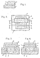
- FIG. 1 is a simplified cross sectional view of a silicon-on-sapphire (SOS) island of the prior art over which a MOSFET is to be fabricated;
- FIG. 2 is a partial top view of the SOS device of FIG. 1 after deposition of oxide layers and conductors;
- FIG. 3 is a cross-sectional view of the silicon island of FIG. 2 taken along lines 3-3 of FIG. 2 and clearly showing the reduced insulation between a polysilicon conductor and the silicon island at the bottom edge corner of the island;
- FIG. 4 is a cross-sectional view of the silicon island of FIG. 2 taken along lines 4-4 of FIG. 2 clearly showing the reduced thickness and poor step coverage of an aluminum conductor;
- FIG. 5 is simplified cross-sectional view of an SOS island similar to that of FIG. 1, illustrating the application of an energy beam according to the method of the present invention;
- FIG. 6 is a partial top view of the SOS device of FIG. 3 after application of the energy beam and after deposition of overlying oxide and metal layers;
- FIG. 7 is a simplified cross-sectional view of the silicon island of FIG. 6 taken along lines 7-7 of FIG. 6 clearly showing the improved insulation between the polysilicon conductor and the silicon island at its bottom edge corner;
- FIG. 8 is a simplified cross-sectional view of the silicon island of FIG. 6 taken along lines 8-8 of FIG. 6 clearly showing the improved step coverage of the aluminum conductor.
- FIG. 1 is a simplified cross sectional view of a silicon on sapphire (SOS) island including a sapphire substrate 1 and a
silicon island 2 photolithographically defined by an etching process to form anisland edge 3. Theisland edge 3 has a steep slope created during definition of thesilicon island 2. - Referring to FIG. 3, a
first oxide layer 6 is preferably grown over the top surface of thesilicon island 2 and the thickness of theoxide layer 6 is reduced at abottom edge corner 8 of the island, forming a "V" shaped groove 9. Thereafter, apolysilicon conductor 10 shown in FIG.'s 2 and 3 is formed by deposition of polycrystalline silicon followed by photolithographic definition and etching. The deposited polysilicon fills the V-shaped groove 9 so that there is a significant likelihood of breakdown conduction between thepolysilicon conductor 10 and thesilicon island 2 in the vicinity of the V-shaped groove 9. - The
polysilicon conductor 10 is deposited, photolithographically defined and etched. Thereafter, the device is ion implanted to render the polysilicon material conductive while simultaneously forming gatealigned source and drain diffusions in thesilicon island 2, in a manner well known in the art. A second layer ofoxide 11 is then placed over the device. Contacts (not shown) are defined through the oxide layers. Analuminium conductor 12 shown in Figures 2 and 4 is formed by evaporation followed by photolithographic definition and etching. Because the etching process which initially defines theedge 3 of theSOS island 2 shown in Figure 1 is not uniform, the resultingisland edge 3 is rough. - Figure 4 clearly shows that the thickness t1 of the
aluminium conductor 12 deposited over thesteep island edge 3 is significantly reduced with respect to the aluminium thickness t2 overlying horizontal surfaces. This reduction of the thickness of thealuminium conductor 12 at theedge 3 increases the probability of discontinuities in theconductor 12. As a result, it has been found that the processing yield of metal-oxide-semi-conductor silicon-on-sapphire (MOS/SOS) devices is significantly reduced. - In the method of the present invention illustrated in Figure 5, a pulsed beam 13 or radiant energy is directed from an energy source 14 such as a laser toward the
silicon island 2 prior to the growth or deposition of overlying insulating and conductive layers. The drawing of Figure 5 is purely schematic and does not imply any restriction on required beam size. The energy beam improves the quality of the crystal structure of thesilicon island 2, which increases the channel mobility of metal oxide semiconductor field effect transistors (MOSFET's) fabricated on thesilicon island 2. It should be noted that, in order to increase mobility, the energy beam may be applied either before or after definition of thesilicon island 2. Mobility in MOS transistors is a well known concept in the art and is discussed, for example, in Penny, et al., MOS Integrated Circuits, Van Nostrand, Reinhold Co., 1972, pages 162-168, the disclosure of which is incorporated by reference. Referring to Figures 7 and 8, anoxide layer 6, apolysilicon conductor 10, asecond oxide layer 11 and analuminium conductor 12 are deposited in the manner described in connection with Figures 1 to 4. - If the energy beam is applied after definition of the
silicon island 2, it causes reflow of silicon in theisland edge 3, and the result is a reformed island edge 3' shown in solid line in Figure 5. The reformed island edge 3' has a moderate slope, being oriented at approximately 60° with respect to the top of the sapphire substrate 1. - Referring to Figure 8, the moderate slope of the island edge 3' permits the deposited
aluminium conduction layer 12 to assume a nearly uniform thickness along the island edge, reducing the likelihood of physical discontinuities in thealuminium conductor 12. - Referring to Figure 7, the likelihood of breakdown conduction at the
bottom edge corner 8 between thepolysilicon conductor 6 and thesilicon island 2 is significantly reduced because the V-shaped groove 9 is eliminated due to the reduced slope of the silicon island edge 3'. In the preferred method of this invention, the energy beam source 14 of Figure 5 is a pulsed excimer laser, emitting a beam 13 having a pulse duration of approximately 25 nanoseconds, a wavelength of approximately 2490A, and an energy density between 0.5 and 1.0 joule/cm2. However, it should be recognized that the scope of this invention includes the use of any pulsed beam source, including an electron, ion or laser beam source in accordance with the present method. The method of this invention is applicable to any MOS/SOS structure similar to that of Figures 6, 7, and 8 in which the first insulating layer is any suitable dielectric, including grown silicon oxide, chemical vapor deposited silicon dioxide, grown silicon nitride, or grown silicon dioxide with chemical vapor deposited silicon nitride. The first insulatinglayer 6 may be grown or deposited silicon dioxide Si02 or silicon nitride (Si3N4) of the type discussed by Pliskin, "Comparison of Properties of Dielectric Films Deposited by Various Methods", Journal of Vacuum Science Technology, Vol. 14, No. 5, September/October 1977, pp. 1064-1081. - The first
conductive layer 10 may be any polycrystalline or amorphous material, such as polycrystalline silicon or it may be polycide or metal silicide of the type disclosed in Crowder et al, "lum MOSFET VLSI Technology: Part VII Metal Silicide Interconnection Technology A Future Prospective", IEEE Trans. on Electron Devices, Vol. Ed.-26 No. 4, April 1979, pages 369-371. Alternatively, theconductive layer 10 may also be a refractory metal layer of the type disclosed in Shah, "Refractory Metal Gate Processes for VLSI Applications", IEEE Trans. on Electron Devices, Vol. ED-26, No. 4, April 1979, pp 631-640. The disclosures of the above-identified Crowder, Shah, and Pliskin Publications are hereby expressly incorporated herein by reference in their entirety. - In summary, this invention is a unique processing technique for improving silicon on sapphire device performance by improving the crystal structure of the silicon islands surface layer to increase channel mobility and thereby improve device operating speed.
Claims (5)
Applications Claiming Priority (3)
| Application Number | Priority Date | Filing Date | Title |
|---|---|---|---|
| US6008179A | 1979-07-24 | 1979-07-24 | |
| US60081 | 1979-07-24 | ||
| EP80901614A EP0032510B1 (en) | 1979-07-24 | 1981-02-09 | Silicon on sapphire laser process |
Related Parent Applications (1)
| Application Number | Title | Priority Date | Filing Date |
|---|---|---|---|
| EP80901614.0 Division | 1981-02-09 |
Publications (3)
| Publication Number | Publication Date |
|---|---|
| EP0171509A2 EP0171509A2 (en) | 1986-02-19 |
| EP0171509A3 EP0171509A3 (en) | 1986-10-29 |
| EP0171509B1 true EP0171509B1 (en) | 1990-10-31 |
Family
ID=26080715
Family Applications (1)
| Application Number | Title | Priority Date | Filing Date |
|---|---|---|---|
| EP85104750A Expired - Lifetime EP0171509B1 (en) | 1979-07-24 | 1980-07-23 | Silicon on sapphire laser process |
Country Status (1)
| Country | Link |
|---|---|
| EP (1) | EP0171509B1 (en) |
Families Citing this family (2)
| Publication number | Priority date | Publication date | Assignee | Title |
|---|---|---|---|---|
| JP2700277B2 (en) | 1990-06-01 | 1998-01-19 | 株式会社半導体エネルギー研究所 | Method for manufacturing thin film transistor |
| US5930608A (en) | 1992-02-21 | 1999-07-27 | Semiconductor Energy Laboratory Co., Ltd. | Method of fabricating a thin film transistor in which the channel region of the transistor consists of two portions of differing crystallinity |
Family Cites Families (2)
| Publication number | Priority date | Publication date | Assignee | Title |
|---|---|---|---|---|
| US4155779A (en) * | 1978-08-21 | 1979-05-22 | Bell Telephone Laboratories, Incorporated | Control techniques for annealing semiconductors |
| DE2848333C2 (en) * | 1978-11-08 | 1984-12-20 | Philips Patentverwaltung Gmbh, 2000 Hamburg | Method for manufacturing a semiconductor component |
-
1980
- 1980-07-23 EP EP85104750A patent/EP0171509B1/en not_active Expired - Lifetime
Also Published As
| Publication number | Publication date |
|---|---|
| EP0171509A3 (en) | 1986-10-29 |
| EP0171509A2 (en) | 1986-02-19 |
Similar Documents
| Publication | Publication Date | Title |
|---|---|---|
| US4341569A (en) | Semiconductor on insulator laser process | |
| EP0037685B1 (en) | Method of producing a semiconductor device | |
| EP0072216B1 (en) | The production of semiconductor devices by methods involving annealing | |
| US4683645A (en) | Process of fabricating MOS devices having shallow source and drain junctions | |
| JP4295922B2 (en) | Gas immersion laser annealing method suitable for application in the fabrication of small integrated circuits | |
| US5077233A (en) | Method for recrystallizing specified portions of a non-crystalline semiconductor material to fabricate a semiconductor device therein | |
| US6387803B2 (en) | Method for forming a silicide region on a silicon body | |
| US5474940A (en) | Method of fabricating a semiconductor device having shallow junctions in source-drain regions and a gate electrode with a low resistance silicide layer | |
| EP0556795B1 (en) | Method of manufacturing substrate having semiconductor on insulator | |
| JP3325992B2 (en) | Method for manufacturing semiconductor device | |
| CA1237828A (en) | Semiconductor-on-insulator (soi) device having electrical short to avoid charge accumulation | |
| US4305973A (en) | Laser annealed double conductor structure | |
| US6740547B2 (en) | Method for fabricating thin-film transistor | |
| US4621411A (en) | Laser-enhanced drive in of source and drain diffusions | |
| US4660276A (en) | Method of making a MOS field effect transistor in an integrated circuit | |
| EP0171509A2 (en) | Silicon on sapphire laser process | |
| EP0032510B1 (en) | Silicon on sapphire laser process | |
| JPH0576176B2 (en) | ||
| US4695856A (en) | Semiconductor device | |
| JPH0677155A (en) | Heat treatment method for semiconductor substrate | |
| JPH03148836A (en) | Manufacture of thin film transistor | |
| KR930011472B1 (en) | Manufacturing method of mos transistor | |
| JPH06204248A (en) | Method for manufacturing MIS transistor | |
| JPH03132041A (en) | Manufacture of semiconductor device | |
| JP2586810B2 (en) | Thin film semiconductor device and method of manufacturing the same |
Legal Events
| Date | Code | Title | Description |
|---|---|---|---|
| PUAI | Public reference made under article 153(3) epc to a published international application that has entered the european phase |
Free format text: ORIGINAL CODE: 0009012 |
|
| AC | Divisional application: reference to earlier application |
Ref document number: 32510 Country of ref document: EP |
|
| AK | Designated contracting states |
Kind code of ref document: A2 Designated state(s): DE FR GB NL |
|
| RAP1 | Party data changed (applicant data changed or rights of an application transferred) |
Owner name: HUGHES AIRCRAFT COMPANY |
|
| RAP1 | Party data changed (applicant data changed or rights of an application transferred) |
Owner name: HUGHES AIRCRAFT COMPANY |
|
| PUAL | Search report despatched |
Free format text: ORIGINAL CODE: 0009013 |
|
| AK | Designated contracting states |
Kind code of ref document: A3 Designated state(s): DE FR GB NL |
|
| 17P | Request for examination filed |
Effective date: 19870408 |
|
| 17Q | First examination report despatched |
Effective date: 19890314 |
|
| GRAA | (expected) grant |
Free format text: ORIGINAL CODE: 0009210 |
|
| AC | Divisional application: reference to earlier application |
Ref document number: 32510 Country of ref document: EP |
|
| AK | Designated contracting states |
Kind code of ref document: B1 Designated state(s): DE FR GB NL |
|
| ET | Fr: translation filed | ||
| REF | Corresponds to: |
Ref document number: 3072182 Country of ref document: DE Date of ref document: 19901206 |
|
| PLBE | No opposition filed within time limit |
Free format text: ORIGINAL CODE: 0009261 |
|
| STAA | Information on the status of an ep patent application or granted ep patent |
Free format text: STATUS: NO OPPOSITION FILED WITHIN TIME LIMIT |
|
| 26N | No opposition filed | ||
| PGFP | Annual fee paid to national office [announced via postgrant information from national office to epo] |
Ref country code: GB Payment date: 19940620 Year of fee payment: 15 |
|
| PGFP | Annual fee paid to national office [announced via postgrant information from national office to epo] |
Ref country code: FR Payment date: 19950612 Year of fee payment: 16 |
|
| PGFP | Annual fee paid to national office [announced via postgrant information from national office to epo] |
Ref country code: DE Payment date: 19950620 Year of fee payment: 16 |
|
| PGFP | Annual fee paid to national office [announced via postgrant information from national office to epo] |
Ref country code: NL Payment date: 19950628 Year of fee payment: 16 |
|
| PG25 | Lapsed in a contracting state [announced via postgrant information from national office to epo] |
Ref country code: GB Effective date: 19950723 |
|
| PG25 | Lapsed in a contracting state [announced via postgrant information from national office to epo] |
Ref country code: NL Effective date: 19960201 |
|
| GBPC | Gb: european patent ceased through non-payment of renewal fee |
Effective date: 19950723 |
|
| NLV4 | Nl: lapsed or anulled due to non-payment of the annual fee |
Effective date: 19960201 |
|
| PG25 | Lapsed in a contracting state [announced via postgrant information from national office to epo] |
Ref country code: FR Effective date: 19970328 |
|
| PG25 | Lapsed in a contracting state [announced via postgrant information from national office to epo] |
Ref country code: DE Effective date: 19970402 |
|
| REG | Reference to a national code |
Ref country code: FR Ref legal event code: ST |