EP0171231A2 - A rearrangeable full availability multistage switching network with redundant conductors - Google Patents
A rearrangeable full availability multistage switching network with redundant conductors Download PDFInfo
- Publication number
- EP0171231A2 EP0171231A2 EP85305267A EP85305267A EP0171231A2 EP 0171231 A2 EP0171231 A2 EP 0171231A2 EP 85305267 A EP85305267 A EP 85305267A EP 85305267 A EP85305267 A EP 85305267A EP 0171231 A2 EP0171231 A2 EP 0171231A2
- Authority
- EP
- European Patent Office
- Prior art keywords
- lre
- network
- stage
- module
- stages
- Prior art date
- Legal status (The legal status is an assumption and is not a legal conclusion. Google has not performed a legal analysis and makes no representation as to the accuracy of the status listed.)
- Granted
Links
Images


Classifications
-
- H—ELECTRICITY
- H04—ELECTRIC COMMUNICATION TECHNIQUE
- H04Q—SELECTING
- H04Q3/00—Selecting arrangements
- H04Q3/64—Distributing or queueing
- H04Q3/68—Grouping or interlacing selector groups or stages
Definitions
- the invention relates to a multistage switching network which is useful in telephonic communication and, in particular, cellular mobile radio-telecommunication systems.
- Rearrangeable switching networks are known in the art, for example, U.S. Pat. Nos. 4,023,141; 3,978,291; 3,358,269; 3,129,407; 3,258,269; 4,038,638 and 4,022,982.
- a rearrangeable full availability network is one in which a successful connection of any idle pair of terminals is guaranteed even though this may require the rearrangement of existing connections. While this same “guarantee” can be achieved in a "strictly nonblocking" network, such networks are larger and more expensive than networks with which the present invention is concerned.
- a service area is typically divided into relatively small "cells," each cell having one or more radio antennae and a base station. All base stations are connected, via land lines to a Mobile Telecommunications Switching Office (MTSO) which serves as the control center for the system and which is also linked to the regular telephone network.
- MTSO Mobile Telecommunications Switching Office
- Mobile calls are initiated by the transmission of source and destination data over special "set-up" channels to the nearest base station which relays the signal to the MTSO.
- the target unit (the number that was dialed) is a land-line telephone
- the MTSO initiates a connection with the regular telephone network after assigning a pair of voice-channels to the mobile unit.
- the target is mobile
- the MTSO circulates a paging signal from one base station to the next until the target is lotated.
- the target responds by transmitting an acknowledgment to its local base station which is then relayed to the MTSO.
- a mobile unit continues to use its assigned pair of channels for as long as it remains within its original (or current). cell. However, when a unit moves from one cell to another, a procedure, referred to as a "hand-off," is initiated. This procedure involves a further data exchange over the special set-up channel, the assignment of a new channel pair and the routing of the call to a new base station.
- the nature of the cellular system is such that it imposes a set of unique and stringent functional requirements on the switching network it employs. Specifically, the network must have full availability so that reconnections made during a hand-off can be guaranteed. For the same reason, the network must be highly reliable and have provisions for detecting and avoiding a faulty path and then detecting and isolating a faulty component for repair.
- reconnections or hand-offs should be transparent to the users, i.e., there should be no telltale discontinuities in ongoing conversations or loss of any data during hand-offs.
- reconnections must be made expeditiously and the design of the system must be such as to facilitate efficient control algorithms.
- the present invention is a multistage rearrangeable, fully available switching network having N T inputs and N. T . outputs.
- the network comprises a plurality of fully available switching elements arranged in an array of stages.
- Inner groups of stages define a plurality of nested modules such that each switch in an outer stage is connected to all associated or subordinate inner modules wherein at least one set of such connections linking stages is redundant.
- the series of nested sets of successively smaller networks which, when the number of stages is odd, typically results in the innermost nesting level being a single switching element and two switching elements when the number is even.
- the network is subdivided into ⁇ stages.
- ⁇ may be either an odd or even integer such that if the number of stages of switches is odd, then ⁇ >3 and if even, then 8 >4.
- Each stage in the network preferably comprises strictly nonblocking switching elements each of which is referred to herein as a Least Reduceable Element (LRE).
- All LRE's in the i-th stage preferably have K. inputs and K i outputs and, thus, have a size K i xK i . If ⁇ is even, there is no general requirement that the LRE's in one stage be equal in size to the LRE's in adjacent stages, except for the I-th and (1+1)-th stages.
- LRE's LRE L (2,1) and LRE R (2,1) are mirror-image LRE's.
- LRE's within and bounded by complementary stages are grouped into one or more subsets, each of which is referred to as a module.
- j designates the module-group comprised of LRE's in stages j to ( ⁇ -j+1), where j ⁇ I.
- each module contains a series of nested sets of successively smaller modules and, such that for 2 ⁇ j ⁇ l, S. is the number of modules of module-group j which nest within a larger module of the (j-1)-th module-group.
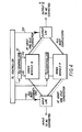
- This arrangement is illustrated in Figure 1.
- Module M(j,k 2 ,k 3 ,...,k j-1 ,k j ) is nested within module M(j-1,k 2 ,k 3 ,...,k j-1 ) thereby making module M(j,k 2 ,k 3 ,...,k j-1 ,k j ) a subordinate module to module M(j-1,k 2 ,k 3 ,..,k j-1 ) and the latter module is a superordinate module to module M(j,k 2 ,k 3 ,...k j-1 ,k j ).
- the I-th module is a single LRE and when ⁇ is even, it is a pair of mirror-image LRE's, and therefore, R l ⁇ 1.
- LRE L (X, k 2 , k 3 ,..., k j ) is the identity of the X-th LRE in the sequence of j-th stage LRE's in module M(j, k 2 , k 3 ,..., k j ), where 1 ⁇ X ⁇ R j .
- LRE R (X,k 2 ,k 3 ,...,k j ) is the identity of the X-th LRE in the sequence of ( ⁇ -j+1)-th stage LRE's in module M(j,k 2 ,k 3 ,...,k j ) where i ⁇ X ⁇ R j .
- LRE L (X,k 2 ,k 3 ,...,k j ) and LRE R (X,k 2 ,k 3 ,...,k j ) are mirror-image LRE's as illustrated in Figure 1.
- each LRE in an outer stage of a superordinate module is linked to all subordinate modules.
- f i is the number of conductors from each module in the subordinate set M(i+1,k 2 ,k 3 ,...,k i ,k i+1 ), linked to each LRE in the set of LRE's LRE R (X,k 2 ,k 3 ,...,k i ), where 1 ⁇ X ⁇ R i .
- any output from any LRE in the I-th stage may be linked to any input to any LRE in the (1 + 1)-th stage, and there is no general requirement that the LRE's so connected be mirror-image LRE's.
- N j is the total number of conductors received by each module in the subordinate set of modules M(j,k 2 ,k 3 ,...,k j-1 ,k j ), where 1 ⁇ k j ⁇ S j , from LRE's in the LRE set LRE L (X,k 2 ,k 3 ,...,k j-1 ), where 1 ⁇ X ⁇ R j-1 .
- N j is the quantity of conductors received by LRE's in LRE set LRE R (X,k 2 ,k 3 ,...,k j-1 ), where 1 ⁇ X ⁇ R j-1 , from each module in the subordinate set of modules M(j,k 2 ,k 3 ,...,k j-1 ,k j ), where 1 ⁇ k j ⁇ S j .
- the entire switching network is itself a module; therefore, by definition, S 1 ⁇ 1 and N 1 ⁇ N T . Furthermore, for the first stage, the notation [A] is defined herein to mean the smallest integer > A.
- Equations (3), (4), (5) and (6) assures a sufficient number of modules and LRE's for full availability as shown hereinafter.
- Equation (3) The importance of redundant conductors on the configuration of the network can be seen in terms of Equation (3) and the recursion obtained by combining Equations (4) and (5), i.e.,
- the compacted network of the present invention has improved performance in terms of a lower probability of having to rearrange existing connections in order to satisfy a new input-to-output assignment, and a larger selection of rearrangements (and, therefore, a potentially simpler rearrangement) when the state of the network is such that the rearrangements cannot be avoided.
- a corresponding rearrangement may not be necessary if f (j-1) > 1.
- f (j-1) the redundant conductors will, in general, increase the total number of sequences available for interchanging the busy connecting paths between modules.
- Equation (13) defines the point of saturation.
- switching network 10 is a rearrangeable, fully available network in which the successful connection of any pair of idle terminals is guaranteed, although this might require the rearrangement of existing connections.
- each stage A through E consists of a series of identical square LRE's 11.
- each LRE 11 within the network 10 is either a single printed circuit board (PCB) or a group of PCB's connected to form a larger LRE 11.
- each LRE 11 in stage B is a PCB with 16 input conductors 13 and 16 output conductors 14.
- output conductors from LRE's 11 in one stage, e . g., A, B, C and D of network 10 are the input conductors to LRE's 11 in the next stages, e.g., B, C, D and E, respectively.
- the 1024 inputs to network 10 pass as 1024 conductors from one stage to the next, terminating at stage E, the last (i.e., fifth) stage, with 1024 outputs.
- the second, third and fourth stages, B, C and D, respectively, taken together, comprise a set of modules 15 which are subordinate to stages A and E.
- the LRE's 11c constitute a series of inner modules 16 which are subordinate to and nested within modules 15.
- the first two conductors 13 and 13' from LRE 11a(1) in the first stage A are to module 15(1); specifically conductor 13 is to LRE 11b(1) and conductor 13' is to LRE 11b(5).
- Modules 15(1)-(8) are indivudually designated as M(2,1),M(2,2),M(2,3),...,M(2,8); and, each module 15 is a fully available, three stage network; see Figure 1.
- the LRE's 11b, 11c and lld, in the second, third and fourth stages, respectively, each have 16 input conductors and 16 output conductors.
- the second stage LRE's 11b in module 15(1) are individually designated as LRE L (1,1),LRE L (2,1),...,LRE L (8,1) and the fourth stage LRE's 11d in module 15(1) are individually designated as LRE R (1,1),LRE R (2,1),...,LRE R (8,1).
- This method of designating LRE's continues in a logical fashion so that the second stage LRE's Ilb in module 15(8) are individually designated as LRE L (1,8),LRE L (2,8),...,LRE R (8,8) and the fourth stage LRE's 11d in module 15(8) are individually designated as LRE R (1,8),LRE R (2,8),...,LRE R (8,8); see Figure 1.
- Each LRE 11c within the center stage C is itself a module 15' and thus receives two conductors 14 and 14' from each of the LRE's in the outer stages B and D of its particular superordinate module 15.
- center stage LRE's 11c in module 15(1) are designated as M(3,1,1),M(3,1,2),...,M(3,1,8) and center stage LRE's 11c in module 15(2) are designated as M(3,2,1),M(3,2,2),...,M(3,2,8).
- This method of designating center stage LRE's 11c continues in a logical fashion so that center stage LRE's 11c in module 15(8) are designated as M(3,8,1), M(3,8,2),...,M(3,8,8).
- a current state-of-the-art network having five stages and 1024 input/outputs would require 256 (16x16) LRE's and 256 (4x4) LRE's. Specifically, it would have 64 (16x16) LRE's in the first and fifth stages; it would have 16 modules at the second nesting level each with four (16x16) LRE's in the second and fourth stages; the third stage within each module would consist of 16 (4x4) elements.
- a state-of-the-art network with comparable network parameters requires more LRE's than the network constructed in accordance with the present invention (i.e., 512 vs. 320).
- the present state-of-the-art networks require two types of LRE's (viz., (16x16) and (4x4)) whereas the networks in accordance with the present invention require only one type (viz., (16x16)).
- the redundant conductors and network compaction of the present invention significantly enhance the overall connectivity of the network. As such, the probability of having to rearrange existing connections in order to accommodate new ones is significantly reduced.
- ICC Inwardly Convergent Control
- a 8-stage network is divided into I domains, where I is given by either Equation (1a) or (1b).
- I is given by either Equation (1a) or (1b).
- D i designates the i-th control domain.
- a control domain is comprised of LRE's in a pair of complementary stages of the network and therefore, for i ⁇ l when 0 is odd, for i ⁇ I when 8 is even, D i is the control domain for the i-th and ( ⁇ -i+1)-th stages. If 8 is odd, then the LRE's in the I-th stage, alone, constitute a control domain, viz., the D domain.
- the first control domain controls the rearrangement of connections between a designated LRE 11a in the first stage of the network, and any of modules 15(1)-(8).
- the first control domain also controls the rearrangement of connections between any of modules 15(1)-(8) and a designated LRE 11d in the fifth stage of the network.
- the second control domain controls the rearrangement of connections between a designated LRE 11b in the second stage within a module 15 and the LRE's 11c in the third stage within the same module 15.
- the second control domain also controls the rearrangement of connections between a designated LRE llc in the third stage of module 15 and the LRE's 11d of the fourth stage within the same module 15.
- the third control domain referred to as D 3 , controls the rearrangement of paths within the center stage LRE's in module 15.
- the ICC methodology rearranges paths starting from the outer stages of the network, moving inward in a symmetric fashion.
- the D i control domain deals only with producing a viable path from designated i-th and ( ⁇ -i+1)-th stage LRE's in superordinate module M(i,k 2 ,k 3 ,...,k i ) to its nested set of subordinate modules M(i+1,k 2 ,k 3 ,...,k i ,k i+1 ), where 1 ⁇ k i+1 ⁇ S i+1 .
- Implementing this path may require that existing connections be rearranged between members of the set of subordinate modules.
- the network of the present invention is such that when this is the case, there is always an inner module (P in Figure 4) with at least one idle conductor to the requested input LRE. Similarly, there is always another inner module (Q in Figure 4) with at least one idle conductor to the requested output LRE.
- a controller can always determine such a pair of inner modules by simply examining a status table that contains input LRE to output LRE link-use information. There is no need to be aware of how exactly the connections are satisfied through the inner modules, because except for the innermost control domains, each inner module will be serviced by its own controller.
- the ICC methodology for rearrangement is the same for each stage of the network. It simply involves exchanging active connecting paths between inner modules (i.e., P and Q in Figure 4) until one of these inner modules has idle conductors to both the requested input and output LRE's. When this is accomplished, control is then transferred to the next inner domain. If 8 is odd, this is repeated until the I-th stage is reached or if 0 is even until I-th and (1 + 1)-th stages are reached, at which point a complete set of rearranged paths through the network has been established and can be implemented. In this regard, it is a feature of this-invention that when rearrangement is required, the redundant conductors will generally increase the total number of available sequences for exchanging active connecting paths between modules.
- Circuits utilizing microprocessors for controlling such rearrangements in accordance with the ICC described above are known to those skilled in the art.
- the networks of the present invention preferably includes a path verification system, and each LRE is provided with a bypass loop to facilitate such testing and fault finding.
- the path verification system as implemented by the network's controllers is as follows:
- LRE 11 comprises a control 16 connected to multiplexer 18 and to (16x16) switch 17 and a tri-state drivers 19 by means of conductors 21, 23 and 24, respectively.
- the sixteen individual input conductors 12 are connected to the (16x16) switch 17 by conductors 12' and to multiplexer 18 by conductors 20. If LRE 11 is in the first stage of the network, then input conductors 12 are from outside network 10; if LRE 11 is not in the first stage, then input conductors 12 are from LRE's 11 in the preceding stages.
- Conductors 13 are the output conductors for the LRE 11 Conductors 13 are connected to the (16x16) switch 17 via conductors 25 and tri-state driver 19(a). If LRE 11 is in the last stage of the network, then output conductors 13 are output from the network; if LRE 11 is not in the last stage, then output conductors 13 are to LRE's 11 in the next stage.
- Conductors 20, 22 and 22', multiplexer 18 and tri-state driver 19(b) consistute the bypass loop which is used for detecting and isolating defective switch 17, described above.
- the (16x16) switch 17 is a strictly nonblocking network; however, it provides for rearrangement of the input or output according to the connection requirements of the next stage.
- the (16x16) switch 17 is composed of 16:1 multiplexers 27(a)-(p); each multiplexer 27 receives 16 conductors 26 which are connected to input conductors 12'.
- the output from each multiplexer 27 is a single conductor 25(a)-(p), which taken together comprise output 25 of the switch 17.
- Control 16 is composed of octal registers 28(a)-(p). These registers 28 are connected to the multiplexers 27 by conductors 29(a)-(p). The control signals to controller 16 are received from the module controller 111 of Figure 4 via conductors 110.
- FIG. 7 depicts a general schematic of a (16x16) PCB 42 which would be combined with 3 others to form a (32x32) LRE 11.
- PCB 42 comprises a (16x16) tri-state output switch 30, a 16:1 multiplexer 33, two quad registers 37 and 38, and two 16 bits registers 39 and 41.
- Input conductors 12 are connected to the tri-state switch 30 by conductors 12' and to multiplexer 33 by conductors 32. If the LRE 11 is in the first stage, then input conductors 12 are from outside the network; otherwise, input conductors 12 are from LRE's 11 in the preceding stage of the network.
- Conductors 44 are the output conductors for PCB 42. Conductors 44 are either connected to another sister component PCB 42 in the LRE 11 or they are connected to an LRE 11 in the next outer stage.
- Conductors 32, 34 and 34', multiplexer 33 and tri-state driver 31 constitute the bypass loop which was described previously; conductors 34' are a 1:16 fan-out of conductor 34.
- Registers 37, 38, 39 and 41 are used to control the bypass loop; the control signals are received from the module controller 111 of Figure 4 via conductors 110.
- LRE 11 is composed of four PCB's 42 and is a strictly nonblocking network; however, it provides for rearrangement of the input or output according to the connection requirements of the next stage.
- the (16x16) PCB is composed of 16:1 multiplexers 46(a)-(p) and tri-state drivers 52(a)-(p).
- Each multiplexer 46 receives 16 conductors 47 which are connected to input conductors 12'. Each multiplexer 46 is connected by a single conductor 45 to a tri-state driver 52. The output from each tri-state driver 52 is a single conductor 43(a)-(p) when, taken together comprise the output 43 of the (16x16) switch 30.
- Control 16' is composed of octal registers 48(a)-(p) and octal registers 50(a)-(d).
- Octal registers 48 are connected to multiplexers 46 by conductors 49(a)-(p);
- octal registers 50 are connected to tri-state drivers 52 by conductors 51 (a)-(p).
- control signals to controller 16' are received from the module controller 111 of Figure 4 via conductors 110.
- Figure 9 is a schematic of a second embodiment of the (16x16) switch 17 of Figure 5.
- the (16x16) switch 17 is a three stage, fully available network composed of twelve (4x4) subelements 17'(a)-(I).
- the input. conductors 12' are distributed equally between the four switches 17'(a), (d), (g) and (j) of the first stage A.
- each switch 17' in the first stage A receives four input conductors 53.
- each switch 17' in the second and third stages, receives four input conductors.
- each switch 17' has four outputs 54; the four sets of these outputs (i.e., 54(a)-(p)), taken together, constitute the output 25 of the (16x16) network 17.
- the (16x16) network 17 obtains its control signals from the module controller 111 of Figure 4 via conductors 110. The appropriate sets of these control signals are passed to each switch element 17' via conductors 55, 56 and 57.
- Figure 10 is a circuit diagram for the (4x4) switch element 17' of Figure 9.
- the switch element consists of D-type flip-flops 58(a)-(j), buffers 59(a)-(g), two-input NAND gates 60(a)-(h), three-input NAND gates 61(a)-(p), two-input AND gates 62(a)-(h) and tri-state drivers 63(a)-(p).
- the four input terminals 53(a)-(d) are connected to buffers 59(d)-(g), respectively; these input terminals are four components of the LRE overall input 12' of Figure 9.
- Control signals are received by switch element 17' at terminals 55, 56, 64 and 57(a)-(e); these terminals are components of the LRE overall control input 110 of Figure 9; the control signals are obtained from the module controller 111 of Figure 4.
- the control signal received at terminal 64 is impressed on buffer 59(c), which initializes D-type flip-flops 58(a)-(j).
- D-type flip-flops 58 control the two-input NAND gates 60(a)-(h) and the three-input NAND gates 61(a)-(p).
- the control signal received at terminal 55 is impressed on buffer 59(a) and loads D-type flip-flops 58(a)-(e) with the signals obtained at terminals 57(a)-(e).
- the control signal received at terminal 56 loads buffer 59(b) which, in turn, loads D-type flip-flops 58(f)-(j) with the signals in flip-flops 58(a)-(e).
- the control signal received at terminal 64 loads buffer 59(c) and is passed to all D-type flip-flops 58.
- the output signals from NAND gates 60(a)-(h) are directed to tri-state drivers 63(a)-(h), respectively, which provide the signals to output terminals 54(a) and 54(d).
- Output terminal 54(a) is connected to tri-state drivers 63(a)-(d) and output terminal 54(d) is connected to tri-state drivers 63(e)-(h).
- the signals from successive pairs of three-input NAND gates 61(a)-(p) are directed to two-input AND gates 62(a)-(h), respectively, and, in turn, are passed to tri-state drivers 63(i)-(p).
- Tri-state drivers 63(i)-(I) are connected to output terminal 54(b) and tri-state drivers 63(m)-(p) are connected to output terminal 54(c).
- the output terminals 54(a)-(d) of switch element 17' are four components of the LRE overall output 25 shown in Figure 9.
- assignments of inputs to outputs often take on a dual form in the sense that if a connection is required between particular, input I p and particular output O v from the network, where 1 ⁇ p ⁇ N T and 1 ⁇ v ⁇ N T , and if p#v, then a corresponding connection is required between input I v and output O p .
- any request for a connection is actually a pair of requests. Since, in any such dual request, the indices of the requested connections are transposed, assignments of this type are referred to as transposed assignments.
- Transposed assignments require that the number of input/output terminals N T be even since otherwise a complete set of dual requests involving all N T inputs and N T outputs cannot be specified.
- i s (j) designate a particular input to an LRE in the j-th stage of the network and let o t (j) designate a particular output from an LRE in the j-th stage where 1 ⁇ s ⁇ K and 1 ⁇ t ⁇ K j .
- Two LRE's in the complementary stages of the network are said to be in transposed states if, for all values of t and s, the LRE in the j-th stage connects i s (j) to o t (j) and the LRE in the ( ⁇ -j+1)-th stage connects i t ( ⁇ -j+1) to o s ( ⁇ -j+1).
- transposed assignments can be realized symmetrically relative to mirror-image LRE's in the sense that, for the realization, mirror-image LRE's can be placed in transposed states.
- a realization of an assignment which has all mirror-image LRE's in transposed states is referred to as a symmetric realization.
- cross-coupling patterns are employed in the present invention. Specifically, when, for 1 ⁇ t ⁇ K l , each o t () is linked to each i t (l+1), then the cross-coupling is said to have an identity pattern. On the other hand, the cross-coupling is said to have a switched pattern when o t (I) is linked to i (t+1) (l+1), for t odd, and when o t (I) is linked to i (t-1) (l+1), for t even.
- Figures 11a and 11b show two implementations of a (32x32) network in 6 stages.
- ⁇ -stage networks with cross-coupling are fully available in that any assignment of inputs to outputs can be realized.
- ⁇ -1)-stage network i.e., a network with an odd number of stages
- ⁇ -stage network i.e., a network with an even number of stages
- R 1 LRE's R 1 LRE's
- a ⁇ -stage network with cross-coupling can symmetrically realize all transposed assignments.
- any such network and one dual request to be realized through it.
- one of the requested pair of requests involves input i x , 1 ⁇ i x ⁇ K 1 , on LRE L (i 1 ), 1 ⁇ i 1 ⁇ R 1 and output o y , 1 ⁇ o y ⁇ K 1 on LRE R (i ⁇ ), 1 ⁇ i ⁇ R 1 .
- Any path can be chosen to satisfy this request.
- Request 1 denote one of the requested connections in the dual request as a required path from input i y , 1 ⁇ i y ⁇ K 1 , on LRE L (i j ), 1 ⁇ i j ⁇ R 1 , to output o x , 1 ⁇ o x ⁇ K 1 , on LRE R (iq), 1 ⁇ i q ⁇ R 1 ;
- Request 2 denote the other requested connection in this dual request.
- a significant enhancement to network connectivity is provided by redundant linkage.
- the cross-coupling between left-side and right-side LRE's in the I-th module grouping is such that if a given path from a network input to some network output goes through module M(k+1,j 2 ,...,j k ,j k+1 ) where jk+l is odd and 1 ⁇ j k+1 ⁇ S k -1 then the dual of this path goes through M(k+1,j 2 ,...,j k ,j k+1 ,+1).
- the single conductors between LRE's in the k-th stage and the M(k+1,j 2 ,...,j k+1 )'s require that two of the M(k+1,j 2 ,...,j k+1 )'s be used to provide a dual path.
- f k ⁇ 2
- only one M(k+1,j 2 ,...,j k+1 ) would be needed to provide such dual paths.
- the availability of dual paths for symmetric realizations of transposed assignments is greater when redundant linkage is used in the network.
- a dual LRE-common control switching element which takes advantage of the network property that mirror-image LRE's can be set to transposed states so as to realize transposed assignments.
- Such a dual element consists of 2 (KxK)-networks and common control logic.
- the same set of control signals which sets one of the (KxK)-networks into a specified state can, with only slight modification, be used to set the mirror-image of that (KxK)-network into the transposed state.
- Figure 12 illustrates the implementation of dual elements in a five stage network.
- Figure 12a illustrates a normal five stage network with LRE's 11A comprising the first stage, 11B comprising the second stage, etc., and with a line of symmetry passing through the third stage; in this example, the signals, shown as arrows, pass from left to right.
- the first and fifth stages are complementary stages and LRE's 11A and 11E are mirror-image LRE's.
- the second and fourth stages are complementary stages and LRE's 11B and 11D are mirror-image LRE's.
- stages 3 and 3' are complementary stages and LRE's llc and 11c' are mirror-image LRE's.
- LRE's llc and 11c' are mirror-image LRE's.
- mirror-image LRE's in stages 1 and 5, 2 and 4 and 3 and 3' share much of the same control logic and circuitry, they are combined into dual switching elements. As illustrated in Figure 12c, this is equivalent to folding the network along the new line of symmetry with the dual elements depicted as 11A/E, 11B/D and 11C/C'. As shown in this example, the network constructed with the dual elements requires only 3/5 of the quantity of control hardware required by the five stage network of Figure 12a. This network, therefore, has N T combined input/output ports. In general, if a is odd, then the comparable fraction would be 1/0, and if ⁇ is even, the fraction would be 1/2.
- Figure 13 is a specific circuit diagram of a (4x4) switch element 17' for LRE 17 of Figure 8 when that type LRE is a dual element.
- the circuit diagram of Figure 13 is the dual-element equivalent of the circuit diagram shown in Figure 10.
- the (4x4) switch element 17' consists of D-type flip-flops 158(a)-(j), buffers 159(a)-(k), two-input NAND gates 160(a)-(h), three-input NAND gates 161(a)-(p), two-input AND gates 162(a)-(h) and tri-state drivers 163(a)-(ff).
- the input terminals 153(a)- : (h) are connected to buffers 159(d)-(k), respectively, these input terminals are components of the LRE overall input 12' of Figure 9.
- Four of the eight input terminals e.g., 153(a)-(d)
- the other four input terminals e.g., 153(e)-(h)
- Control signals are received by switch element 17' at terminals 155, 156, 164 and 157(a)-(e). These terminals are components of the LRE overall control input 110 of Figure 9. The control signals are obtained from the module controller 111 of Figure 4.
- the control signal received at terminal 164 is impressed on buffer 159(c) and passes to D-type flip-flops 158(a)-(j).
- D-type flip-flops 158 control the two-input NAND gates 160(a)-(h) and the three-input NAND gates 161(a)-(p).
- the control signal received at terminal 155 is impressed on buffer 159(a) and passes to D-type flip-flops 158(a)-(e); similarly, the control signal received at terminal 156 loads buffers 159(b) and passes to D-type flip-flops 158(f)-(j).
- the control signal received at terminal 164 loads buffers 159(c) and passes to all D-type flip-flops 158.
- the output signals from NAND gates 160(a)-(d) are directed to tri-state driver pairs 163(a) and (g), 163(b) and (u), 163(c) and (y) and 163(d) and (cc), respectively.
- the output signals from NAND gates 160(e)-(h) are directed to tri-state driver pairs 163(m) and (t), 163(n) and (x), 163(o) and (bb) and 163(p) and (ff).
- the signals from successive pairs of three-input NAND gates 161(a)-(p) are directed to two-input AND gates 162(a)-(h), respectively.
- the signals from two-input AND gates 162(a)-(h) are directed to tri-state driver pairs 163(e) and (r), 163(f) and (v), 163(g) and (z), 163(h) and (dd), 163(i) and (s), 163(j) and (w), 163(k) and (aa) and 163(1) and (ee) respectively.
- Tri-state drivers 163(a)-(d) are connected to output terminal 154(a), drivers 163(e)-(h) to 154(b), drivers 163(i)-(I) to terminal 154(c), drivers 163(m)-(p) to terminal 154(d), drivers 163(q)-(t) to terminal 154(e), drivers 163(u)-(x) to terminal 154(f), drivers 163(y)-(bb) to terminal 154(g) and driver 163(ce) to terminal 154(h).
- Input signals received on terminals 153(a)-(d) are passed to any of output terminals 154(a)-(d) and the input signals received on terminals 153(e)-(h) are passed to any of output terminal 154(e)-(h).
- the output terminals 154(a)-(h) of switch element 17' are components of the LRE overall output 25 of Figure 9.
- Four of the eight output terminals (e.g., 154(a)-(d)) are part of LRE 11A/E(1) of Figure 11(c) while the other four output terminals (e.g., 154(e)-(h)) are part of LRE A/E(5) of Figure 11 (c).
Abstract
Description
- The invention relates to a multistage switching network which is useful in telephonic communication and, in particular, cellular mobile radio-telecommunication systems. Rearrangeable switching networks are known in the art, for example, U.S. Pat. Nos. 4,023,141; 3,978,291; 3,358,269; 3,129,407; 3,258,269; 4,038,638 and 4,022,982.
- A rearrangeable full availability network is one in which a successful connection of any idle pair of terminals is guaranteed even though this may require the rearrangement of existing connections. While this same "guarantee" can be achieved in a "strictly nonblocking" network, such networks are larger and more expensive than networks with which the present invention is concerned.
- The requirements of cellular mobile telecommunications place additional demands on the switching network employed in such systems. In a cellular system, a service area is typically divided into relatively small "cells," each cell having one or more radio antennae and a base station. All base stations are connected, via land lines to a Mobile Telecommunications Switching Office (MTSO) which serves as the control center for the system and which is also linked to the regular telephone network.
- Mobile calls are initiated by the transmission of source and destination data over special "set-up" channels to the nearest base station which relays the signal to the MTSO. If the target unit (the number that was dialed) is a land-line telephone, the MTSO initiates a connection with the regular telephone network after assigning a pair of voice-channels to the mobile unit. If the target is mobile, the MTSO circulates a paging signal from one base station to the next until the target is lotated. The target responds by transmitting an acknowledgment to its local base station which is then relayed to the MTSO.
- A mobile unit continues to use its assigned pair of channels for as long as it remains within its original (or current). cell. However, when a unit moves from one cell to another, a procedure, referred to as a "hand-off," is initiated. This procedure involves a further data exchange over the special set-up channel, the assignment of a new channel pair and the routing of the call to a new base station.
- In normal telephone systems, once a connection is made it remains in effect until the conversation is terminated. On the other hand, due to hand-offs, the connecting paths in the cellular system are frequently broken and remade while the conversation is in progress. Clearly, therefore, the nature of the cellular system is such that it imposes a set of unique and stringent functional requirements on the switching network it employs. Specifically, the network must have full availability so that reconnections made during a hand-off can be guaranteed. For the same reason, the network must be highly reliable and have provisions for detecting and avoiding a faulty path and then detecting and isolating a faulty component for repair. Also, the reconnections or hand-offs should be transparent to the users, i.e., there should be no telltale discontinuities in ongoing conversations or loss of any data during hand-offs. Finally, reconnections must be made expeditiously and the design of the system must be such as to facilitate efficient control algorithms.
- In the current state-of-the-art networks, all of the performance objectives associated with cellular radio-telecommunications cannot be achieved, or if achieved, the networks are relatively large and expensive and/or their architectures do not facilitate expeditious reconnections nor do they facilitate efficient control algorithms. Moreover, the state-of-the-art networks do not readily accommodate additions to their subscriber/user base. For example, in such a network having N T input/output terminals, additions to the network normally increase by a rate proportional to NT.log2(NT), rather than linearly with NT.
- It is, therefore, an objective of the present invention to provide a rearrangeable fully available switching network useful for both voice and data transmission that meets all of the functional requirements of a cellular mobile radio-telecommunications system, but which can also be used in Private Automatic Branch Exchange (PABX) systems. Specifically, it is an objective of the invention:
- (1) to provide a general multistage network configuration predicated on the use of redundant conductors between stages which, when compared to state-of-the-art networks, greatly reduces the probability of having to rearrange existing connections in order to connect an idle pair of terminals and which simplifies the process when rearrangement is required;
- (2) to provide a network configuration which facilitates path verification through the network and which facilitates the process of locating and isolating faulty components;
- (3) to provide conformable specific embodiments of the general network in which the least reducible element is a printed circuit board and in which all of the printed circuit boards are identical, throughout the network;
- (4) to provide conformable specific embodiments of the general network which permit the growth of the network, in terms of such printed circuit boards, to be directly proportional to the total number of input and output terminals required;
- (5) to provide conformable specific embodiments of the general network which permit the use of such printed circuit boards which are dual switching elements each of which consists of two disjoint elements with a common controller to effectively reduce the total number of such printed circuit boards by approximately one-half.
- The present invention is a multistage rearrangeable, fully available switching network having NT inputs and N.T. outputs. The network comprises a plurality of fully available switching elements arranged in an array of stages. Inner groups of stages define a plurality of nested modules such that each switch in an outer stage is connected to all associated or subordinate inner modules wherein at least one set of such connections linking stages is redundant. In the present invention, the series of nested sets of successively smaller networks which, when the number of stages is odd, typically results in the innermost nesting level being a single switching element and two switching elements when the number is even. In considering the description of the invention it is useful to refer to Figure 1 to more fully understand the nesting concept.
- The network is subdivided into θ stages. In the present invention, θ may be either an odd or even integer such that if the number of stages of switches is odd, then θ >3 and if even, then 8 >4. In describing the network, "i" is used to designate any stage in the network, where i=1,2,3,...,8. I is used to designate the center stage when 8 is odd, such that
-


- Each stage in the network preferably comprises strictly nonblocking switching elements each of which is referred to herein as a Least Reduceable Element (LRE). All LRE's in the i-th stage preferably have K. inputs and Ki outputs and, thus, have a size KixKi. If θ is even, there is no general requirement that the LRE's in one stage be equal in size to the LRE's in adjacent stages, except for the I-th and (1+1)-th stages.
- If θ is odd, then, for i < I and if θ is even, then for i < the i-th stage of the network is the mirror-image of the (θ-i+1)-th stage and stages i and (θ-i+1) are said to be complementary stages. All LRE's in complementary stages are of equal size and Ki=K(θ-i+1). Likewise, LRE's occupying mirror-image positions in complementary stages are said to be mirror-image LRE's. Thus, for example, in Figure 1, LRE's LREL(2,1) and LRER(2,1) are mirror-image LRE's.
- In the present invention, LRE's within and bounded by complementary stages are grouped into one or more subsets, each of which is referred to as a module. As used herein, j designates the module-group comprised of LRE's in stages j to (θ-j+1), where j≤I.
- If θ is odd, then each LRE in the I-th stage is also a module which belongs to module-group j=l. If θ is even, then the' j=l-th module-group is a pair of LRE's.
- Each module in the j-th module-group is itself a fully available square switching network having (θ-2j+2) stages, N. inputs and Nj outputs, and, if j=I, then Nl≡Kl.
- The number and configurations of the LRE's within all modules of the j-th module-group are identical and therefore, all modules in module-group j are said to be identical.
- The entire switching network is deemed to be a module which is designated the
j =1 module-group. Where 1 ≤ j ≤ I, each module contains a series of nested sets of successively smaller modules and, such that for 2 ≤ j ≤ l, S. is the number of modules of module-group j which nest within a larger module of the (j-1)-th module-group. - M(j, k2, k3,..,kj-1,kj) is the identity of the kj-th module in the j-th module-group which nests within the k(j-1)-th module of module-group (j-1), which nests within..., which nests within the k2-th module of module-group j=2 where, for all j, 1 ≤ kj ≤ Sj. This arrangement is illustrated in Figure 1.
- Module M(j,k2,k3,...,kj-1,kj) is nested within module M(j-1,k2,k3,...,kj-1) thereby making module M(j,k2,k3,...,kj-1,kj) a subordinate module to module M(j-1,k2,k3,..,kj-1) and the latter module is a superordinate module to module M(j,k2,k3,...kj-1,kj).
- Where 1 ≤ i ≤ l, Rl is the number of LRE's comprising the i-th stage of the network which are contained within each module of module-group j=i. By reason of symmetry, Ri is the number of LRE's comprising the (θ-i+1)-th stage of the network which are contained within each module of module-group j=i. Furthermore, if 8 is odd, the I-th module is a single LRE and when θ is even, it is a pair of mirror-image LRE's, and therefore, Rl≡1.
- For j < I (θ is odd) or j ≤ l (0 is even), LREL(X, k2, k3,..., kj) is the identity of the X-th LRE in the sequence of j-th stage LRE's in module M(j, k2, k3,..., kj), where 1≤X≤Rj. On the other hand, for j > I (θ is odd) or j≥(i+1) (θ is even) LRER(X,k2,k3,...,kj) is the identity of the X-th LRE in the sequence of (θ-j+1)-th stage LRE's in module M(j,k2,k3,...,kj) where i≤X≤Rj. Thus, the pair of LRE's, LREL(X,k2,k3,...,kj) and LRER(X,k2,k3,...,kj) are mirror-image LRE's as illustrated in Figure 1.
- If θ is odd, then, since each LRE in the I-th stage is a module, the pivot LRE's have the singular designation M(l,k2,k3,...,kl), where 1≤kl≤Sl.
- In the present invention each LRE in an outer stage of a superordinate module is linked to all subordinate modules. The number of conductors from each LRE, when i≤l, in the set of LRE's LREL(X,k2,k3,...,ki), for 1≤X≤Ri, linked to each module in the subordinate set of modules M(i+1, k2, k3, ..., ki, ki+1) where 1≤ki+1≤Si+1 is fi. Similarly, for i≤l, fi is the number of conductors from each module in the subordinate set M(i+1,k2,k3,...,ki,ki+1), linked to each LRE in the set of LRE's LRER(X,k2,k3,...,ki), where 1≤X≤Ri.
- Figure 1 illustrates a linkage pattern in which
f j=2 for all values of i. However, as described hereinafter,-only one set of conductors needs to be greater than 1. When fi is greater than 1, those conductors are said to be identified redundant conductors. - If 8 is even, any output from any LRE in the I-th stage may be linked to any input to any LRE in the (1+1)-th stage, and there is no general requirement that the LRE's so connected be mirror-image LRE's.
- If θ is odd, each module in module-group j=I-1 is a three stage network and Sl is the number of LRE's within the center stage of each of the three stage modules. Accordingly, it is a particular feature of this invention that R(l-1)≡Sl=R(l+1), when 8 is odd.
- For 2≤j≤l, Nj is the total number of conductors received by each module in the subordinate set of modules M(j,k2,k3,...,kj-1,kj), where 1≤kj≤Sj, from LRE's in the LRE set LREL(X,k2,k3,...,kj-1), where 1≤X≤Rj-1. Similarly, when 2≤j≤1, Nj is the quantity of conductors received by LRE's in LRE set LRER(X,k2,k3,...,kj-1), where 1≤X≤Rj-1, from each module in the subordinate set of modules M(j,k2,k3,...,kj-1,kj), where 1≤kj≤Sj.
- As discussed previously, the entire switching network is itself a module; therefore, by definition, S1≡1 and N1≡NT. Furthermore, for the first stage,

the notation [A] is defined herein to mean the smallest integer > A. - When 2≤i≤l, the distributions of the modules, inter-module conductors and intra-module LRE's, respectively, are given by the equations


- In order that the network have full availability, the following necessary condition must prevail for 1≤i≤l:

- Furthermore, the satisfaction of Equations (3), (4), (5) and (6) assures a sufficient number of modules and LRE's for full availability as shown hereinafter.
- RT is the total number of LRE's used to construct the network such that based on the nesting concept,

where Ψ=l-1, when 8 is odd and Ψ=I, when 0 is even and ξ=1, when θ is odd and ξ=0 and when 8 is even. - The importance of redundant conductors on the configuration of the network can be seen in terms of Equation (3) and the recursion obtained by combining Equations (4) and (5), i.e.,

- Thus, for any i<I, when fi>l, the required number of modules in module-group j=
i +1 is reduced according to Equation (3) relative to the situation where fi=1 and the number of LRE's in each module of the j-th module-group and in all of their subsequent subordinate modules increases according to Equation (8). This decrease in the number of modules in the j-th module group according to Equation (3) is referred to as compaction. The result of compaction is to provide a significantly more powerful connectivity to the network. This connectivity distinguishes the present invention from those of the prior art. - The increase in connectivity resulting from compaction is readily apparent when compared to known, fully available, networks that do not use compaction (i.e., f.=1, 1≤i≤l-1) but satisfy Equation (3), such as the state-of-the-art networks described by V. E. Benes in "Mathematical Theory of Connecting Networks for Telephone Traffic" Academic Press (1965).*
- * Suppose that for a present state of the art network, some f., for 1≤i≤l-1, is increased to, say, 2. In other words, in the original design,
f i =1, but in the new design, fi=2. This means that in the new network S'i+1=[Ki/2] and N'i+1=2Ni+1. Hence the (i+1)-th module-group in the new network consists of approximately one-half of the number of modules of the original network, where each of these modules M(i+1,k2,k3,...,ki,ki+1), is itself a fully available subnetwork of size (2Ni+1x2Ni+1) to which each LREL(X, k2,..., ki) has fi=2 links and from which each LRER(X,k2,...,ki) receives fi=2 links. Because of the full availability of the original network and because each of the modules of the (i+1)-th module-group is also a fully available subnetwork, the new network is fully available. Extending the above argument to the more general case where more than one fi>1 is straightforward. Hence, compacted networks satisfying Equations (3) through (6) are fully available. - Equally important to retaining full availability, the compacted network of the present invention has improved performance in terms of a lower probability of having to rearrange existing connections in order to satisfy a new input-to-output assignment, and a larger selection of rearrangements (and, therefore, a potentially simpler rearrangement) when the state of the network is such that the rearrangements cannot be avoided. For example, for any j-th module-group, when f and a rearrangement between modules is necessary, a corresponding rearrangement may not be necessary if f(j-1) > 1. However, if there is no need to rearrange when f(j-1)>1, there may still exist a need if f(j-1)=1. Furthermore, when f(j-1) > 1 and a rearrangement between modules of the j-th module-group is necessary, the redundant conductors will, in general, increase the total number of sequences available for interchanging the busy connecting paths between modules.
- Combining Equations (3), (7) and (8), yields for the total number of LRE's in a general compacted network as follows:

- In a preferred embodiment of the present invention the LRE's in all stages of the network are of equal size such that, for all values of 1≤i≤l, Ki =K, and K and NT have values such that


- Subject to these conditions, the size of Equation (9) is directly proportional to the number of stages and to the number of input/output terminals, namely,


- Typical growth curves for networks derived from the principles of the present invention and subject to the constraints of Equations (10) and (11) are shown in Figure 2; these curves are for 6=3, 5 and 7 and for K=8, 16 and 32.
- The characteristics and advantages of the network of the present invention will become apparent from a perusal of the detailed description of the presently preferred embodiments taken in connection with the accompanying drawings.
-
- Figure 1 shows a general compacted network illustrating the designations of modules and LRE's;
- Figure 2 shows the growth curves described by Equation (12);
- Figure 3 is a general schematic drawing of a five stage compacted network using redundant conductors;
- Figure 4 is a general schematic of the control for networks of the present invention;
- Figure 5 is a general schematic of a (16x16) LRE;
- Figure 6 is one specific circuit diagram for a PCB for a (16x16) LRE;
- Figure 7 is a general schematic of a (16x16) PCB which is to be combined with others to make a (32x32) LRE;
- Figure 8 is one specific circuit diagram for the (16x16) PCB of Figure 7;
- Figure 9 is a general schematic of a (16x16) LRE comprised of a three stage, rearrangeable network of (4x4) switch elements;
- Figure 10 is one specific circuit diagram for the (4x4) switch element of the LRE shown in Figure 9;
- Figure 11a and b illustrate the cross-coupling in two implementations of a (32x32) six stage network.
- Figure 12a-c illustrates the implementation of dual elements in a five stage symmetrical network.
- Figure 13 is one specific circuit diagram for the (4x4) switch element of the LRE shown in Figure 9 when that LRE is a dual element.
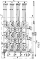
- Referring to Figure 3, switching
network 10 is a rearrangeable, fully available network in which the successful connection of any pair of idle terminals is guaranteed, although this might require the rearrangement of existing connections. - In the specific embodiment of Figure 3, there are 1024 inputs to and 1024 outputs from the network (i.e., NT=1024), five stages (i.e., θ=5); each stage A through E consists of a series of identical square LRE's 11.
- According to the invention, each
LRE 11 within thenetwork 10 is either a single printed circuit board (PCB) or a group of PCB's connected to form alarger LRE 11. In this particular embodiment, eachLRE 11 in stage A is a PCB with 16input conductors LRE 11 in stage B is a PCB with 16input conductors output conductors 14. As can be seen, output conductors from LRE's 11 in one stage, e.g., A, B, C and D ofnetwork 10 are the input conductors to LRE's 11 in the next stages, e.g., B, C, D and E, respectively. Thus, the 1024 inputs to network 10 pass as 1024 conductors from one stage to the next, terminating at stage E, the last (i.e., fifth) stage, with 1024 outputs. - The number of LRE's 11 in outer stages A and E is computed by dividing the total number of input/outputs to the network by the number of terminal connections on a single LRE (i.e., R1=R5=1024/16=64).
- The LRE's 11A(1)-(64) in the first stage are individually designated LREL(1), LRE. (2),...,LREL (64), respectively, and the LRE's IID(1)-(64) are individually designated LRER(1),LRER(2),...,LRER(64), respectively; see Figure 1.
- In the five stage embodiment of
network 10 the second, third and fourth stages, B, C and D, respectively, taken together, comprise a set ofmodules 15 which are subordinate to stages A and E. In the third stage, C, the LRE's 11c constitute a series ofinner modules 16 which are subordinate to and nested withinmodules 15. - As shown in Figure 3, there are two conductors between each LRE in the first and fifth stages, A and E, respectively, and each next inner subordinate module 15 (i.e., f.=2). For example, the first two
conductors 13 and 13' from LRE 11a(1) in the first stage A are to module 15(1); specificallyconductor 13 is to LRE 11b(1) and conductor 13' is to LRE 11b(5). - Since there are two
conductors 13 and 13' from each outer LRE 11a to eachsubordinate module 15 then there are 8 of these subordinate modules 15(1)-(8) required (i.e.,S 2=16/2=8). - Modules 15(1)-(8), respectively, are indivudually designated as M(2,1),M(2,2),M(2,3),...,M(2,8); and, each
module 15 is a fully available, three stage network; see Figure 1. - The number of input/outputs to network 10 are distributed equally among the modules 15(1)-(8) so that each of these
modules 15 receives 128conductors 13 and 13' from the LRE's lla in the first stage A (i.e., N2 =2(64)=128). - Within each
module 15, the LRE's 11b, 11c and lld, in the second, third and fourth stages, respectively, each have 16 input conductors and 16 output conductors. - The total number of conductors received by each module 15 (i.e., N2 128) are distributed equally among the LRE's llb and lld in each module's outer stages (i.e., the second and fourth stages, B and D, respectively). Thus, eight LRE's 11b and 11d are required in both stages B and D of each module 14 (i.e., R2=R4=128/16=8).
- The second stage LRE's 11b in module 15(1) are individually designated as LREL(1,1),LREL(2,1),...,LREL(8,1) and the fourth stage LRE's 11d in module 15(1) are individually designated as LRER(1,1),LRER(2,1),...,LRER(8,1). This method of designating LRE's continues in a logical fashion so that the second stage LRE's Ilb in module 15(8) are individually designated as LREL(1,8),LREL(2,8),...,LRER(8,8) and the fourth stage LRE's 11d in module 15(8) are individually designated as LRER (1,8),LRER(2,8),...,LRER(8,8); see Figure 1.
- Each LRE 11c within the center stage C is itself a module 15' and thus receives two
conductors 14 and 14' from each of the LRE's in the outer stages B and D of its particularsuperordinate module 15. Thus, eight LRE's llc(1)-(8) are required in the center stage of each module 15 (i.e.,S 3 =16/2=8). - The center stage LRE's 11c in module 15(1) are designated as M(3,1,1),M(3,1,2),...,M(3,1,8) and center stage LRE's 11c in module 15(2) are designated as M(3,2,1),M(3,2,2),...,M(3,2,8). This method of designating center stage LRE's 11c continues in a logical fashion so that center stage LRE's 11c in module 15(8) are designated as M(3,8,1), M(3,8,2),...,M(3,8,8).
- The total number of LRE's 11 required to construct the compacted
network 10 is 320, i.e., RT=((2)(64)+8(12x8)+8)=320. - In comparison, a current state-of-the-art network having five stages and 1024 input/outputs would require 256 (16x16) LRE's and 256 (4x4) LRE's. Specifically, it would have 64 (16x16) LRE's in the first and fifth stages; it would have 16 modules at the second nesting level each with four (16x16) LRE's in the second and fourth stages; the third stage within each module would consist of 16 (4x4) elements.
- As shown by the preceding specific examples, a state-of-the-art network with comparable network parameters (i.e., NT=1024 and 8=5) requires more LRE's than the network constructed in accordance with the present invention (i.e., 512 vs. 320). Furthermore, the present state-of-the-art networks require two types of LRE's (viz., (16x16) and (4x4)) whereas the networks in accordance with the present invention require only one type (viz., (16x16)). Furthermore, the redundant conductors and network compaction of the present invention significantly enhance the overall connectivity of the network. As such, the probability of having to rearrange existing connections in order to accommodate new ones is significantly reduced.
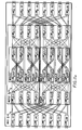
- The inherent connectivity of
network 10 due to the redundant conductors provided between stages significantly reduces the need for the rearrangement of paths of existing connections to satisfy a new connection demand. However, when rearrangement of the existing paths must take place, there are a number of possible rearrangement strategies which the network supports. Referring to Figures 3 and 4, a presently preferred control is referred to as the Inwardly Convergent Control (ICC). - According to the ICC methodology, a 8-stage network is divided into I domains, where I is given by either Equation (1a) or (1b). For i ≤l, Di designates the i-th control domain.
- A control domain is comprised of LRE's in a pair of complementary stages of the network and therefore, for i≤l when 0 is odd, for i < I when 8 is even, Di is the control domain for the i-th and (θ-i+1)-th stages. If 8 is odd, then the LRE's in the I-th stage, alone, constitute a control domain, viz., the D domain.
- For example, referring to Figure 3, there are three control domains in the five
stage network 10. The first control domain, referred to as D1, controls the rearrangement of connections between a designated LRE 11a in the first stage of the network, and any of modules 15(1)-(8). The first control domain also controls the rearrangement of connections between any of modules 15(1)-(8) and a designated LRE 11d in the fifth stage of the network. - The second control domain, referred to as D2, controls the rearrangement of connections between a designated LRE 11b in the second stage within a
module 15 and the LRE's 11c in the third stage within thesame module 15. The second control domain also controls the rearrangement of connections between a designated LRE llc in the third stage ofmodule 15 and the LRE's 11d of the fourth stage within thesame module 15. - The third control domain, referred to as D3, controls the rearrangement of paths within the center stage LRE's in
module 15. - The ICC methodology rearranges paths starting from the outer stages of the network, moving inward in a symmetric fashion. Thus, for i <1, the Di, control domain deals only with producing a viable path from designated i-th and (θ-i+1)-th stage LRE's in superordinate module M(i,k2,k3,...,ki) to its nested set of subordinate modules M(i+1,k2,k3,...,ki,ki+1), where 1≤ki+1≤Si+1. Implementing this path may require that existing connections be rearranged between members of the set of subordinate modules.
- Within each affected module of the subordinate set of modules M(i+1,k2,k3,...,ki,ki+1), where 1≤ki+1≤Si+1, the prior connection problem is now in the Di+1 control domain. This domain deals only with producing a viable path from the affected (i+1)-th and (θ-i)-th stage LRE's in affected modules to their nested set of subordinate modules M(
i +2,k2,k3,...,ki, ki+1,ki+2), where 1≤ki+2≤Si+2. - If 6 is odd then, repeating this process I times, results in the rearrangement converging inwardly to the I-th stage (or to the I-th and (1+1)-th stages when 8 is even) where it is finally completely solved in the Dl control demain.
- As the rearrangement problem converges inward between complementary pairs of stages of LRE's, there is a natural partitioning of the problem that takes place which permits the resulting disjoint parts to be solved concurrently. For example, in the D. control domain, a rearrangement of existing paths can be determined that demands a further rearrangement of existing paths of some subset of the Sj+1 subordinate modules. The rearrangements within each of these subordinate modules can be done concurrently since they are confined exclusively to within their own subordinate modules. Thus, in any j-th set of subordinate modules, there are S. controllers, one for each module in the set. Each such controller solely considers the rearrangement of paths between the R. LRE's in the input stage of the module and the R. LRE's in its output stage. Preferably, at the innermost control domains, the connection problem is so finely partitioned that one controler is able to efficiently serve multiple inner modules.
- Relative to a given domain of control, a rearrangement is only required when no subordinate module has idle conductors between the input LRE and output LRE to which a connecting path is requested. As shown in Figure 4, the network of the present invention, is such that when this is the case, there is always an inner module (P in Figure 4) with at least one idle conductor to the requested input LRE. Similarly, there is always another inner module (Q in Figure 4) with at least one idle conductor to the requested output LRE. A controller can always determine such a pair of inner modules by simply examining a status table that contains input LRE to output LRE link-use information. There is no need to be aware of how exactly the connections are satisfied through the inner modules, because except for the innermost control domains, each inner module will be serviced by its own controller.
- The ICC methodology for rearrangement is the same for each stage of the network. It simply involves exchanging active connecting paths between inner modules (i.e., P and Q in Figure 4) until one of these inner modules has idle conductors to both the requested input and output LRE's. When this is accomplished, control is then transferred to the next inner domain. If 8 is odd, this is repeated until the I-th stage is reached or if 0 is even until I-th and (1+1)-th stages are reached, at which point a complete set of rearranged paths through the network has been established and can be implemented. In this regard, it is a feature of this-invention that when rearrangement is required, the redundant conductors will generally increase the total number of available sequences for exchanging active connecting paths between modules.
- Circuits utilizing microprocessors for controlling such rearrangements in accordance with the ICC described above are known to those skilled in the art.
- Normally, in rearrangeable, fully available networks, faulty paths remain concealed by the large number of alternate paths available for connecting an idle pair of terminals. Thus, if a fault exists, it must be isolated and identified for repair or replacement. Therefore, the networks of the present invention preferably includes a path verification system, and each LRE is provided with a bypass loop to facilitate such testing and fault finding.
- The path verification system as implemented by the network's controllers is as follows:
- (1) when an input-to-output connection is requested a path through the network is determined;
- (2) a test signal from the input terminal is transmitted over the path to the output terminal;
- (3) if the test signal is correctly received, the users are connected into the network;
- (4) if the test signal fails to be received correctly at the output, another path through the switching network is determined and the identity of the LRE's comprising the faulty path are recorded for subsequent testing;
- (5) the defective LRE is isolated and identified by transmitting a test'signal over the faulty path and, one by one, shunting the test signal via each LRE's bypass loop.
- With reference to Figure 5, a general schematic of an
LRE 11 is shown.LRE 11 comprises acontrol 16 connected to multiplexer 18 and to (16x16) switch 17 and atri-state drivers 19 by means ofconductors - The sixteen
individual input conductors 12 are connected to the (16x16) switch 17 by conductors 12' and to multiplexer 18 byconductors 20. IfLRE 11 is in the first stage of the network, then inputconductors 12 are fromoutside network 10; ifLRE 11 is not in the first stage, then inputconductors 12 are from LRE's 11 in the preceding stages. -
Conductors 13 are the output conductors for theLRE 11Conductors 13 are connected to the (16x16) switch 17 viaconductors 25 and tri-state driver 19(a). IfLRE 11 is in the last stage of the network, thenoutput conductors 13 are output from the network; ifLRE 11 is not in the last stage, thenoutput conductors 13 are to LRE's 11 in the next stage. -
Conductors multiplexer 18 and tri-state driver 19(b) consistute the bypass loop which is used for detecting and isolatingdefective switch 17, described above. - Referring to Figure 6, a specific circuit diagram for a (16x16)
LRE 11 is shown. In this embodiment, the (16x16) switch 17 is a strictly nonblocking network; however, it provides for rearrangement of the input or output according to the connection requirements of the next stage. - In this embodiment, the (16x16) switch 17 is composed of 16:1 multiplexers 27(a)-(p); each multiplexer 27 receives 16 conductors 26 which are connected to input conductors 12'. The output from each multiplexer 27 is a single conductor 25(a)-(p), which taken together comprise
output 25 of theswitch 17. -
Control 16 is composed of octal registers 28(a)-(p). These registers 28 are connected to the multiplexers 27 by conductors 29(a)-(p). The control signals tocontroller 16 are received from the module controller 111 of Figure 4 viaconductors 110. - Figure 7 depicts a general schematic of a (16x16)
PCB 42 which would be combined with 3 others to form a (32x32)LRE 11.PCB 42 comprises a (16x16)tri-state output switch 30, a 16:1multiplexer 33, twoquad registers -
Input conductors 12 are connected to thetri-state switch 30 by conductors 12' and to multiplexer 33 byconductors 32. If theLRE 11 is in the first stage, then inputconductors 12 are from outside the network; otherwise,input conductors 12 are from LRE's 11 in the preceding stage of the network. -
Conductors 44 are the output conductors forPCB 42.Conductors 44 are either connected to anothersister component PCB 42 in theLRE 11 or they are connected to anLRE 11 in the next outer stage. -
Conductors multiplexer 33 andtri-state driver 31 constitute the bypass loop which was described previously; conductors 34' are a 1:16 fan-out ofconductor 34. -
Registers conductors 110. - Referring to Figure 8, a specific circuit diagram for
PCB 42 is shown. In this embodiment,LRE 11 is composed of four PCB's 42 and is a strictly nonblocking network; however, it provides for rearrangement of the input or output according to the connection requirements of the next stage. - In this embodiment, the (16x16) PCB is composed of 16:1 multiplexers 46(a)-(p) and tri-state drivers 52(a)-(p).
- Each
multiplexer 46 receives 16 conductors 47 which are connected to input conductors 12'. Eachmultiplexer 46 is connected by a single conductor 45 to atri-state driver 52. The output from eachtri-state driver 52 is a single conductor 43(a)-(p) when, taken together comprise theoutput 43 of the (16x16)switch 30. - Control 16' is composed of octal registers 48(a)-(p) and octal registers 50(a)-(d). Octal registers 48 are connected to multiplexers 46 by conductors 49(a)-(p);
octal registers 50 are connected totri-state drivers 52 by conductors 51 (a)-(p). - The control signals to controller 16' are received from the module controller 111 of Figure 4 via
conductors 110. - Figure 9 is a schematic of a second embodiment of the (16x16) switch 17 of Figure 5. In this embodiment, the (16x16) switch 17 is a three stage, fully available network composed of twelve (4x4) subelements 17'(a)-(I).
- The input. conductors 12' are distributed equally between the four switches 17'(a), (d), (g) and (j) of the first stage A. Thus, each switch 17' in the first stage A receives four
input conductors 53. Similarly, each switch 17' in the second and third stages, (i.e., B and C, respectively) receives four input conductors. - Pursuant to the logic of rearrangeable, fully available networks, each switch 17' has four
outputs 54; the four sets of these outputs (i.e., 54(a)-(p)), taken together, constitute theoutput 25 of the (16x16)network 17. - The (16x16)
network 17 obtains its control signals from the module controller 111 of Figure 4 viaconductors 110. The appropriate sets of these control signals are passed to each switch element 17' viaconductors - Figure 10 is a circuit diagram for the (4x4) switch element 17' of Figure 9. In this embodiment, the switch element consists of D-type flip-flops 58(a)-(j), buffers 59(a)-(g), two-input NAND gates 60(a)-(h), three-input NAND gates 61(a)-(p), two-input AND gates 62(a)-(h) and tri-state drivers 63(a)-(p).
- The four input terminals 53(a)-(d) are connected to buffers 59(d)-(g), respectively; these input terminals are four components of the LRE overall input 12' of Figure 9.
- Control signals are received by switch element 17' at
terminals overall control input 110 of Figure 9; the control signals are obtained from the module controller 111 of Figure 4. - As shown in Figure 10, the control signal received at
terminal 64 is impressed on buffer 59(c), which initializes D-type flip-flops 58(a)-(j). D-type flip-flops 58 control the two-input NAND gates 60(a)-(h) and the three-input NAND gates 61(a)-(p). The control signal received atterminal 55 is impressed on buffer 59(a) and loads D-type flip-flops 58(a)-(e) with the signals obtained at terminals 57(a)-(e). Similarly, the control signal received at terminal 56 loads buffer 59(b) which, in turn, loads D-type flip-flops 58(f)-(j) with the signals in flip-flops 58(a)-(e). The control signal received at terminal 64 loads buffer 59(c) and is passed to all D-type flip-flops 58. - The output signals from NAND gates 60(a)-(h) are directed to tri-state drivers 63(a)-(h), respectively, which provide the signals to output terminals 54(a) and 54(d). Output terminal 54(a) is connected to tri-state drivers 63(a)-(d) and output terminal 54(d) is connected to tri-state drivers 63(e)-(h).
- The signals from successive pairs of three-input NAND gates 61(a)-(p) (e.g., 61(a), (b); 61(c), (d); etc.) are directed to two-input AND gates 62(a)-(h), respectively, and, in turn, are passed to tri-state drivers 63(i)-(p).
- Tri-state drivers 63(i)-(I) are connected to output terminal 54(b) and tri-state drivers 63(m)-(p) are connected to output terminal 54(c).
- The output terminals 54(a)-(d) of switch element 17' are four components of the LRE
overall output 25 shown in Figure 9. - In switching networks, assignments of inputs to outputs often take on a dual form in the sense that if a connection is required between particular, input Ip and particular output Ov from the network, where 1≤p≤NT and 1≤v≤NT, and if p#v, then a corresponding connection is required between input Iv and output Op. In such a case, any request for a connection is actually a pair of requests. Since, in any such dual request, the indices of the requested connections are transposed, assignments of this type are referred to as transposed assignments.
- Transposed assignments require that the number of input/output terminals NT be even since otherwise a complete set of dual requests involving all NT inputs and NT outputs cannot be specified.
- Let is(j) designate a particular input to an LRE in the j-th stage of the network and let ot(j) designate a particular output from an LRE in the j-th stage where 1 < s < K and 1≤t≤Kj.
- Two LRE's in the complementary stages of the network are said to be in transposed states if, for all values of t and s, the LRE in the j-th stage connects is(j) to ot(j) and the LRE in the (θ-j+1)-th stage connects it(θ-j+1) to os(θ-j+1).
- In 0-stage networks of the present invention, where 8 is even and where K1,K2,...,Kl are all even, transposed assignments can be realized symmetrically relative to mirror-image LRE's in the sense that, for the realization, mirror-image LRE's can be placed in transposed states. A realization of an assignment which has all mirror-image LRE's in transposed states is referred to as a symmetric realization.
- To achieve symmetric realizations of all transposed assignments in networks where θ is even requires that the LRE's in the I-th stage be linked in a particular way to the LRE's in the (1+1)-th stage and that the linkage need not necessarily be between mirror-image LRE's. Such linking patterns will be referred to as cross-couplings.
- Depending on the nature of the conductor-redundancy parameters, f1,f2,...,fl-1, two cross-coupling patterns are employed in the present invention. Specifically, when, for 1≤t≤Kl, each ot() is linked to each it(l+1), then the cross-coupling is said to have an identity pattern. On the other hand, the cross-coupling is said to have a switched pattern when ot(I) is linked to i(t+1)(l+1), for t odd, and when ot(I) is linked to i(t-1)(l+1), for t even.
- If, for all values of 1≤j≤(l-1), fj>1, then the pair of mirror-image LRE's comprising each M(l,k2,k3,...,kl) module are cross-coupled according to the switched linking pattern.
- If, for some value of j, fj=1 and for any 1≤i≤(j-1), fi >1, then c=j+1 is the index of module-group across which cross-coupling must occur if the symmetric realization of all network assignments are to be achieved. In this case LREL(1,k2,k3,...,kc=a,...,kl) is cross-coupled to LRER(1,k2,k3,...,kc=b,...,kl) using the identity linking pattern and, likewise, LREL(1,k2,k3,...,kc=b,...,kl) is cross-coupled to LRER(1,k2,k3,...,kc=a,...,kl), where (a,b) designates the ordered pairs (1,2),(3,4),...,(Sc-1,Sc).
- As an example of the cross-coupling described above, Figures 11a and 11b show two implementations of a (32x32) network in 6 stages. In each network Ki=4,
i =1,...,6. In Figure 11a, f1=2 andf 2 =1. Hence, the cross-coupling is the identity linking pattern between LREL(1,k2,a) and LRER(1,k2,b), and between LREL(1,k2,b) and LRER(1,k2,a), for k2=1, 2 and (a,b)=(1,2),(3,4). In Figure 11b, f1=1 andf 2=2. Hence, the cross-coupling is the identity linking pattern between LREL(1,a,k3) and LRER(1,b,k3), and between LREL(1,b,k3) and LRER(1,a,k3) fork - In the present invention θ-stage networks with cross-coupling, as described above, are fully available in that any assignment of inputs to outputs can be realized. To demonstrate the full availability, consider a fully available (θ-1)-stage network (i.e., a network with an odd number of stages) which can be transformed into a θ-stage network (i.e., a network with an even number of stages) by adding a new stage between the I-th and the (l+1)-th stages by cutting the links between the I-th and the (I+1)-th stages and inserting R1 LRE's; setting the linking between the LRE's of this new stage and the LRE's in (what was previously) the (l+1)-th stage to be a replica of that between the LRE's in (what were previously) the I-th and (l+1)-th stages; and setting the linking between LRE's between the 1-th stage and the new stage to correspond to the cross-coupling described above. Because all LRE's have full connectivity between their Kl inputs and Kl outputs, it is clear that for such cross-coupling, the addition of a new stage in this manner does not affect the full connectivity of the original network.
- Moreover, a θ-stage network with cross-coupling, as described above, can symmetrically realize all transposed assignments. To demonstrate this, consider any such network and one dual request to be realized through it. Suppose without any loss of generality, that one of the requested pair of requests involves input ix, 1≤ix≤K1, on LREL(i1), 1≤i1≤R1 and output oy, 1≤oy≤K1 on LRER(iθ), 1≤i≤R1. Any path can be chosen to satisfy this request. It should be noted that establishing a second path by setting the mirror-image LRE of each LRE in the other path into the transposed state results in a path from input iy on LRER(iθ) to output ox on LRER(i1). In other words, this second path satisfies the other request in the original dual request. These two paths will be referred to as dual paths. Hence, symmetric realization in a θ-stage network with cross-coupling as described above is assured via dual paths for a single dual request. Assume this is true for any w dual requests, i≤w<(NT/2); that is, the symmetric realization via dual paths are assured for any w or fewer dual requests. To show then that this is true for any w+1 dual requests, it will suffice to assume otherwise and see that this leads to a contradiction. Accordingly, assume that there is a set of w dual requests that can be symmetrically realized via dual paths through the network, but assume this realization places the network into a state in which an additional dual request cannot also be symmetrically realized.
Let Request 1 denote one of the requested connections in the dual request as a required path from input iy, 1≤iy≤K1, on LREL(ij), 1≤ij≤R1, to output ox, 1≤ox≤K1, on LRER(iq), 1≤iq≤R1; letRequest 2 denote the other requested connection in this dual request. By assumption for the given state of the network, any additional path through thenetwork satisfying Request 1 is such that its dual cannot be used to satisfyRequest 2. Likewise, any additional path through thenetwork satisfying Request 2 is such that its dual cannot be used to satisfyRequest 1. But therein lies a contradiction: for if the network is satisfying w dual requests via w dual paths and additionallyRequest 1 can be satisfied by some path but the dual of this path is not available to satisfyRequest 2, it must be that one of w dual paths is using a segment of this dual path. But the dual of this segment must also be used which means that the path used to satisfyRequest 1 could not have been available to begin with. Hence a 8-stage network with cross-coupling as described above can symmetrically realize all transposed assignments. - A significant enhancement to network connectivity is provided by redundant linkage. For example, in a network where
f k =1 andf - In accordance with the present invention, it is possible to provide a dual LRE-common control switching element which takes advantage of the network property that mirror-image LRE's can be set to transposed states so as to realize transposed assignments. Such a dual element consists of 2 (KxK)-networks and common control logic. The same set of control signals which sets one of the (KxK)-networks into a specified state can, with only slight modification, be used to set the mirror-image of that (KxK)-network into the transposed state.
- Figure 12 illustrates the implementation of dual elements in a five stage network. In this example, Figure 12a illustrates a normal five stage network with LRE's 11A comprising the first stage, 11B comprising the second stage, etc., and with a line of symmetry passing through the third stage; in this example, the signals, shown as arrows, pass from left to right.
- In Figure 12a, the first and fifth stages are complementary stages and LRE's 11A and 11E are mirror-image LRE's. Similarly, the second and fourth stages are complementary stages and LRE's 11B and 11D are mirror-image LRE's.
- By using dual elements, one effectively adds another stage to the network, shown as stage 3' in Figure 12b, thus shifting the line of symmetry. In Figure 12b, stages 3 and 3' are complementary stages and LRE's llc and 11c' are mirror-image LRE's. For simplicity, it is assumed in Figure 12, that f1>1 and f2>1 and therefore, a switched cross-coupling pattern is shown.
- Since mirror-image LRE's in
stages - Figure 13 is a specific circuit diagram of a (4x4) switch element 17' for
LRE 17 of Figure 8 when that type LRE is a dual element. Thus, the circuit diagram of Figure 13 is the dual-element equivalent of the circuit diagram shown in Figure 10. - In a dual element embodiment, the (4x4) switch element 17' consists of D-type flip-flops 158(a)-(j), buffers 159(a)-(k), two-input NAND gates 160(a)-(h), three-input NAND gates 161(a)-(p), two-input AND gates 162(a)-(h) and tri-state drivers 163(a)-(ff).
- The input terminals 153(a)-:(h) are connected to buffers 159(d)-(k), respectively, these input terminals are components of the LRE overall input 12' of Figure 9. Four of the eight input terminals (e.g., 153(a)-(d)) are part of LRE 11A/E(1) of Figure 10c while the other four input terminals (e.g., 153(e)-(h)) are part of LRE A/E(5) of Figure 10c.
- Control signals are received by switch element 17' at
terminals overall control input 110 of Figure 9. The control signals are obtained from the module controller 111 of Figure 4. - As shown in Figure 12, the control signal received at
terminal 164 is impressed on buffer 159(c) and passes to D-type flip-flops 158(a)-(j). D-type flip-flops 158 control the two-input NAND gates 160(a)-(h) and the three-input NAND gates 161(a)-(p). The control signal received atterminal 155 is impressed on buffer 159(a) and passes to D-type flip-flops 158(a)-(e); similarly, the control signal received at terminal 156 loads buffers 159(b) and passes to D-type flip-flops 158(f)-(j). The control signal received atterminal 164, loads buffers 159(c) and passes to all D-type flip-flops 158. - The output signals from NAND gates 160(a)-(d) are directed to tri-state driver pairs 163(a) and (g), 163(b) and (u), 163(c) and (y) and 163(d) and (cc), respectively. The output signals from NAND gates 160(e)-(h) are directed to tri-state driver pairs 163(m) and (t), 163(n) and (x), 163(o) and (bb) and 163(p) and (ff).
- The signals from successive pairs of three-input NAND gates 161(a)-(p) (e.g., 161(a), (b); 161(c), (d); etc.) are directed to two-input AND gates 162(a)-(h), respectively.
- The signals from two-input AND gates 162(a)-(h) are directed to tri-state driver pairs 163(e) and (r), 163(f) and (v), 163(g) and (z), 163(h) and (dd), 163(i) and (s), 163(j) and (w), 163(k) and (aa) and 163(1) and (ee) respectively.
- Tri-state drivers 163(a)-(d) are connected to output terminal 154(a), drivers 163(e)-(h) to 154(b), drivers 163(i)-(I) to terminal 154(c), drivers 163(m)-(p) to terminal 154(d), drivers 163(q)-(t) to terminal 154(e), drivers 163(u)-(x) to terminal 154(f), drivers 163(y)-(bb) to terminal 154(g) and driver 163(ce) to terminal 154(h).
- Input signals received on terminals 153(a)-(d) are passed to any of output terminals 154(a)-(d) and the input signals received on terminals 153(e)-(h) are passed to any of output terminal 154(e)-(h). The output terminals 154(a)-(h) of switch element 17' are components of the LRE
overall output 25 of Figure 9. Four of the eight output terminals (e.g., 154(a)-(d)) are part of LRE 11A/E(1) of Figure 11(c) while the other four output terminals (e.g., 154(e)-(h)) are part of LRE A/E(5) of Figure 11 (c). - While the presently preferred embodiments of the invention have been shown and described in particularity, the invention may be otherwise embodied within the scope of the appended claims.
Claims (10)

and

the number of LRE's comprising said network is directly proportional to N T such that

where
said LRE is the least reducible element in the network.
Applications Claiming Priority (2)
| Application Number | Priority Date | Filing Date | Title |
|---|---|---|---|
| US06/636,913 US4654842A (en) | 1984-08-02 | 1984-08-02 | Rearrangeable full availability multistage switching network with redundant conductors |
| US636913 | 1984-08-02 |
Publications (3)
| Publication Number | Publication Date |
|---|---|
| EP0171231A2 true EP0171231A2 (en) | 1986-02-12 |
| EP0171231A3 EP0171231A3 (en) | 1988-10-05 |
| EP0171231B1 EP0171231B1 (en) | 1993-01-27 |
Family
ID=24553866
Family Applications (1)
| Application Number | Title | Priority Date | Filing Date |
|---|---|---|---|
| EP85305267A Expired - Lifetime EP0171231B1 (en) | 1984-08-02 | 1985-07-24 | A rearrangeable full availability multistage switching network with redundant conductors |
Country Status (6)
| Country | Link |
|---|---|
| US (1) | US4654842A (en) |
| EP (1) | EP0171231B1 (en) |
| JP (1) | JPH0638673B2 (en) |
| CA (1) | CA1236553A (en) |
| DE (1) | DE3587028T2 (en) |
| SG (1) | SG110194G (en) |
Cited By (6)
| Publication number | Priority date | Publication date | Assignee | Title |
|---|---|---|---|---|
| EP0396816A2 (en) * | 1989-05-12 | 1990-11-14 | Siemens Aktiengesellschaft | Multi-stage switching network |
| US5581688A (en) * | 1993-04-29 | 1996-12-03 | Telefonaktiebolaget Lm Ericsson | Tele- and data communication system |
| GB2304255A (en) * | 1995-08-07 | 1997-03-12 | Be Aerospace Inc | Multi-stage switch |
| GB2344254A (en) * | 1995-08-07 | 2000-05-31 | Be Aerospace Inc | Rearrangeable multi-stage switch |
| DE19849776B4 (en) * | 1997-12-31 | 2006-07-13 | Samsung Electronics Co., Ltd., Suwon | Scalable multilevel interconnect network architecture and method for performing an expansion of that architecture during operation |
| GB2430326A (en) * | 2005-09-16 | 2007-03-21 | Tyco Electronics Raychem Nv | Cross connect device comprising a plurality of sparse cross bars |
Families Citing this family (25)
| Publication number | Priority date | Publication date | Assignee | Title |
|---|---|---|---|---|
| US4862161A (en) * | 1985-01-24 | 1989-08-29 | Ant Nachrichtentechnik Gmbh | Three-stage coupling arrangement |
| US4804956A (en) * | 1986-03-31 | 1989-02-14 | General Signal Corporation | Rearrangeable digital signal space division switching system |
| GB2188813B (en) * | 1986-04-01 | 1990-03-14 | Stc Plc | Switching network |
| LU87005A1 (en) * | 1987-02-20 | 1988-02-02 | Siemens Ag | COUPLING ARRANGEMENT FOR MULTI-STAGE COUPLING PANELS IN TELECOMMUNICATION SWITCHING SYSTEMS, IN PARTICULAR TIME MULTIPLEX TELEPHONE SWITCHING SYSTEMS, WITH COUPLING MULTIPLE AND THESE FROM COUPLING LEVEL TO COUPLING LEVEL |
| US4817083A (en) * | 1987-03-06 | 1989-03-28 | American Telephone And Telegraph Company At&T Bell Laboratories | Rearrangeable multiconnection switching networks employing both space division and time division switching |
| GB8705771D0 (en) * | 1987-03-11 | 1987-04-15 | Plessey Co Plc | Synchronisation arrangements |
| US4970505A (en) * | 1987-04-09 | 1990-11-13 | Nec Corporation | Three stage switching apparatus |
| US4833468A (en) * | 1987-10-14 | 1989-05-23 | Unisys Corporation | Layered network |
| US4845722A (en) * | 1987-10-16 | 1989-07-04 | Digital Equipment Corporation | Computer interconnect coupler employing crossbar switching |
| DE3802579A1 (en) * | 1988-01-29 | 1989-08-10 | Ant Nachrichtentech | THREE-STAGE NON-BLOCKING DOMESTIC |
| US5198808A (en) * | 1988-09-20 | 1993-03-30 | Nec Corporation | Matrix switch apparatus with a diagnosis circuit having stand-by ports and reduced size matrix switching elements |
| US5128929A (en) * | 1988-11-15 | 1992-07-07 | Nec Corporation | Time division switching system capable of broad band communications service |
| US4952930A (en) * | 1988-11-18 | 1990-08-28 | International Business Machines Corp. | Multipath hierarchical network |
| US5023864A (en) * | 1989-05-08 | 1991-06-11 | At&T Bell Laboratories | Crossover network utilizing two-dimensional arrays of nodes |
| DE4020775A1 (en) * | 1989-08-09 | 1991-02-14 | Standard Elektrik Lorenz Ag | COUPLING NETWORK AND COUPLING NETWORK MODULE FOR AN ATM SYSTEM |
| JP2836135B2 (en) * | 1989-11-10 | 1998-12-14 | 松下電器産業株式会社 | Method for producing catalytic functional material |
| US5216420A (en) * | 1990-07-12 | 1993-06-01 | Munter Ernst A | Matrix sorting network for sorting N inputs onto N outputs |
| US5229990A (en) * | 1990-10-03 | 1993-07-20 | At&T Bell Laboratories | N+K sparing in a telecommunications switching environment |
| US5654695A (en) * | 1991-02-22 | 1997-08-05 | International Business Machines Corporation | Multi-function network |
| FR2718909B1 (en) * | 1994-04-18 | 1996-06-28 | Transpac | Connection matrix electrically configurable between lines of at least one input / output port for electrical signals. |
| DE4415016A1 (en) * | 1994-04-29 | 1995-11-02 | Sel Alcatel Ag | Process for operating a switching network and switching network and switching center therefor |
| US5495476A (en) * | 1995-01-26 | 1996-02-27 | International Business Machines Corporation | Parallel algorithm to set up benes switch; trading bandwidth for set up time |
| US6088329A (en) * | 1997-12-11 | 2000-07-11 | Telefonaktiebolaget Lm Ericsson | Fault tolerant subrate switching |
| US20030063839A1 (en) * | 2001-05-11 | 2003-04-03 | Scott Kaminski | Fault isolation of individual switch modules using robust switch architecture |
| US6951941B2 (en) * | 2003-02-06 | 2005-10-04 | Com Dev Ltd. | Bi-planar microwave switches and switch matrices |
Citations (1)
| Publication number | Priority date | Publication date | Assignee | Title |
|---|---|---|---|---|
| GB1567477A (en) * | 1976-10-01 | 1980-05-14 | Danray Inc | Digital switching for telephone communication systems |
Family Cites Families (7)
| Publication number | Priority date | Publication date | Assignee | Title |
|---|---|---|---|---|
| FR2041351A5 (en) * | 1969-04-22 | 1971-01-29 | Labo Cent Telecommunicat | |
| US3760103A (en) * | 1971-12-02 | 1973-09-18 | Bell Telephone Labor Inc | Bidirectional storage crosspoint matrices for mirror image time division switching systems |
| FR2311470A1 (en) * | 1975-05-13 | 1976-12-10 | Thomson Csf | TIME-SWITCHED PABX, METHODS FOR RECONFIGURING SUCH A PABX |
| US4198546A (en) * | 1976-01-23 | 1980-04-15 | Siemens Aktiengesellschaft | Time division multiplex switching network |
| US4038638A (en) * | 1976-06-01 | 1977-07-26 | Bell Telephone Laboratories, Incorporated | Efficient rearrangeable multistage switching networks |
| CA1065977A (en) * | 1977-05-09 | 1979-11-06 | Real Gagnier | Switching network for a pcm tdm system |
| JPS5726955A (en) * | 1980-07-25 | 1982-02-13 | Hitachi Ltd | Backup control system |
-
1984
- 1984-08-02 US US06/636,913 patent/US4654842A/en not_active Expired - Lifetime
-
1985
- 1985-07-12 CA CA000486707A patent/CA1236553A/en not_active Expired
- 1985-07-24 EP EP85305267A patent/EP0171231B1/en not_active Expired - Lifetime
- 1985-07-24 DE DE8585305267T patent/DE3587028T2/en not_active Expired - Lifetime
- 1985-08-01 JP JP60168663A patent/JPH0638673B2/en not_active Expired - Fee Related
-
1994
- 1994-08-08 SG SG110194A patent/SG110194G/en unknown
Patent Citations (1)
| Publication number | Priority date | Publication date | Assignee | Title |
|---|---|---|---|---|
| GB1567477A (en) * | 1976-10-01 | 1980-05-14 | Danray Inc | Digital switching for telephone communication systems |
Non-Patent Citations (6)
| Title |
|---|
| IEEE TRANSACTIONS ON COMPUTERS, vol. C-31, no. 5, May 1982, pages 443-454, IEEE, New York, US; G.B. ADAMS et al.: "The extra stage cube: a fault-tolerant interconnection network for supersystems" * |
| INTERNATIONAL CONFERENCE ON COMMUNICATIONS, Chicago, 12th-15th June 1977, vol. 1, paper 10.6, pages 244-248, IEEE, New York, US; G. KAMPE: "Analysis of link systems with delay" * |
| PROCEEDINGS OF THE INTERNATIONAL SWITCHING SYMPOSIUM, Florence, 7th-11th May 1984, part I, session 23C, paper 2, pages 1-6, North-Holland, Amsterdam, NL; U. KILLAT et al.: "System aspects and components for broadband switching" * |
| PROCEEDINGS OF THE INTERNATIONAL SYMPOSIUM ON THE THEORY OF SWITCHING, part II, anuals 30, 1959, pages 235-240, President and Fellows of Harvard College, Harvard University, Cambridge, GB; B.D. HOLBROOK: "Some logical requirements for the control of switching networks" * |
| TELECOMMUNICATIONS AND RADIO ENGINEERING, vol. 25/26, no. 11, November 1971, pages 35-42, Washington, US; L.A. BASSALYGO et al.: "Nonblocking structures for undivided switching systems" * |
| THE 7TH ANNUAL SYMPOSIUM ON COMPUTER ARCHITECTURE, Long Beach, 6th-8th May 1980, Proceedings of the annual symposium on computer architecture, pages 190-195, IEEE, New York, US; D. NASSIMI et al.: "A self routing benes network" * |
Cited By (10)
| Publication number | Priority date | Publication date | Assignee | Title |
|---|---|---|---|---|
| EP0396816A2 (en) * | 1989-05-12 | 1990-11-14 | Siemens Aktiengesellschaft | Multi-stage switching network |
| EP0396816A3 (en) * | 1989-05-12 | 1991-03-20 | Siemens Aktiengesellschaft | Multi-stage switching network |
| US5414706A (en) * | 1989-05-12 | 1995-05-09 | Siemens Aktiengesellschaft | Multi-stage switching equipment |
| US5581688A (en) * | 1993-04-29 | 1996-12-03 | Telefonaktiebolaget Lm Ericsson | Tele- and data communication system |
| GB2304255A (en) * | 1995-08-07 | 1997-03-12 | Be Aerospace Inc | Multi-stage switch |
| GB2304255B (en) * | 1995-08-07 | 2000-04-12 | Be Aerospace Inc | Multi-stage switch |
| GB2344254A (en) * | 1995-08-07 | 2000-05-31 | Be Aerospace Inc | Rearrangeable multi-stage switch |
| GB2344254B (en) * | 1995-08-07 | 2000-07-19 | Be Aerospace Inc | Multi-stage switch |
| DE19849776B4 (en) * | 1997-12-31 | 2006-07-13 | Samsung Electronics Co., Ltd., Suwon | Scalable multilevel interconnect network architecture and method for performing an expansion of that architecture during operation |
| GB2430326A (en) * | 2005-09-16 | 2007-03-21 | Tyco Electronics Raychem Nv | Cross connect device comprising a plurality of sparse cross bars |
Also Published As
| Publication number | Publication date |
|---|---|
| CA1236553A (en) | 1988-05-10 |
| DE3587028T2 (en) | 1993-07-01 |
| JPH0638673B2 (en) | 1994-05-18 |
| US4654842A (en) | 1987-03-31 |
| JPS6143093A (en) | 1986-03-01 |
| SG110194G (en) | 1994-11-25 |
| DE3587028D1 (en) | 1993-03-11 |
| EP0171231B1 (en) | 1993-01-27 |
| EP0171231A3 (en) | 1988-10-05 |
Similar Documents
| Publication | Publication Date | Title |
|---|---|---|
| US4654842A (en) | Rearrangeable full availability multistage switching network with redundant conductors | |
| US4901309A (en) | Cross-connect for switch modules | |
| US3920914A (en) | Divided time-division switching network | |
| US4400627A (en) | Telephone switching network | |
| EP0363822B1 (en) | Broadcast network | |
| US4293946A (en) | Trilateral duplex path conferencing system with broadcast capability | |
| US4550398A (en) | Modular self-routing PCM switching network for distributed-control telephone exchange | |
| US4945534A (en) | Programmable conferencing module for ring arrays and switchable ring array networks | |
| US4025725A (en) | Telecommunication switching network having a multistage reversed trunking scheme and switching on a four wire basis | |
| CA1204845A (en) | Modular self-routing pcm switching network for distributed control telephone exchanges | |
| US3106615A (en) | Communication switching system | |
| US3740480A (en) | Time division multiplex switching system utilizing all time division techniques | |
| US4045617A (en) | Telecommunication switching network having a multistage reversed trunking arrangement | |
| US2853552A (en) | Trunking diagram for an automatic telecommunication system | |
| Uematsu et al. | Architecture of a packet switch based on banyan switching network with feedback loops | |
| US4420832A (en) | Concentrator-deconcentrator devices | |
| FI74860B (en) | KOPPLINGSFAELT MED FOERBINDELSEOMKASTNING, SAERSKILT FOER TELEFONCENTRALER. | |
| US3657486A (en) | Time division multiplex pax of the four wire type | |
| US3649768A (en) | High capacity switching network and control arrangement | |
| US3542970A (en) | Crossbar switching system with relatively uniform growth characteristics | |
| US3406259A (en) | Switching contact network having common multiple primary switch means | |
| FI78208C (en) | KOPPLINGSANORDNING FOER EN TELEFONCENTRAL, SAERSKILT EN TELEFONVAEXEL MED TAL- OCH SIGNALGENOMKOPPLING OEVER SERIEKOPPLADE OMKOPPLARE. | |
| US6411619B1 (en) | Remotely reconfigurable switching network | |
| RU2119263C1 (en) | Digital switching system | |
| US3730974A (en) | Signalling network for automatic telecommunication switching system |
Legal Events
| Date | Code | Title | Description |
|---|---|---|---|
| PUAI | Public reference made under article 153(3) epc to a published international application that has entered the european phase |
Free format text: ORIGINAL CODE: 0009012 |
|
| AK | Designated contracting states |
Designated state(s): CH DE FR GB IT LI NL SE |
|
| PUAL | Search report despatched |
Free format text: ORIGINAL CODE: 0009013 |
|
| AK | Designated contracting states |
Kind code of ref document: A3 Designated state(s): CH DE FR GB IT LI NL SE |
|
| 17P | Request for examination filed |
Effective date: 19890321 |
|
| 17Q | First examination report despatched |
Effective date: 19910506 |
|
| GRAA | (expected) grant |
Free format text: ORIGINAL CODE: 0009210 |
|
| STAA | Information on the status of an ep patent application or granted ep patent |
Free format text: STATUS: THE PATENT HAS BEEN GRANTED |
|
| AK | Designated contracting states |
Kind code of ref document: B1 Designated state(s): CH DE FR GB IT LI NL SE |
|
| REF | Corresponds to: |
Ref document number: 3587028 Country of ref document: DE Date of ref document: 19930311 |
|
| ET | Fr: translation filed | ||
| ITF | It: translation for a ep patent filed |
Owner name: SOCIETA' ITALIANA BREVETTI S.P.A. |
|
| PLBE | No opposition filed within time limit |
Free format text: ORIGINAL CODE: 0009261 |
|
| 26N | No opposition filed | ||
| ITTA | It: last paid annual fee | ||
| EAL | Se: european patent in force in sweden |
Ref document number: 85305267.8 |
|
| REG | Reference to a national code |
Ref country code: GB Ref legal event code: IF02 |
|
| PGFP | Annual fee paid to national office [announced via postgrant information from national office to epo] |
Ref country code: NL Payment date: 20040916 Year of fee payment: 20 |
|
| PGFP | Annual fee paid to national office [announced via postgrant information from national office to epo] |
Ref country code: FR Payment date: 20040920 Year of fee payment: 20 |
|
| PGFP | Annual fee paid to national office [announced via postgrant information from national office to epo] |
Ref country code: SE Payment date: 20040921 Year of fee payment: 20 |
|
| PGFP | Annual fee paid to national office [announced via postgrant information from national office to epo] |
Ref country code: GB Payment date: 20040922 Year of fee payment: 20 |
|
| PGFP | Annual fee paid to national office [announced via postgrant information from national office to epo] |
Ref country code: CH Payment date: 20040924 Year of fee payment: 20 |
|
| PGFP | Annual fee paid to national office [announced via postgrant information from national office to epo] |
Ref country code: DE Payment date: 20040930 Year of fee payment: 20 |
|
| PG25 | Lapsed in a contracting state [announced via postgrant information from national office to epo] |
Ref country code: GB Free format text: LAPSE BECAUSE OF EXPIRATION OF PROTECTION Effective date: 20050723 |
|
| PG25 | Lapsed in a contracting state [announced via postgrant information from national office to epo] |
Ref country code: NL Free format text: LAPSE BECAUSE OF EXPIRATION OF PROTECTION Effective date: 20050724 |
|
| REG | Reference to a national code |
Ref country code: CH Ref legal event code: PL |
|
| REG | Reference to a national code |
Ref country code: GB Ref legal event code: PE20 |
|
| EUG | Se: european patent has lapsed | ||
| NLV7 | Nl: ceased due to reaching the maximum lifetime of a patent |
Effective date: 20050724 |